Author Topic: MEMS - nice die pictures  (Read 6845 times)

0 Members and 1 Guest are viewing this topic.

Offline NoopyTopic starter

  • Super Contributor
  • ***
  • Posts: 1726
  • Country: de
    • Richis-Lab
MEMS - nice die pictures
« on: February 10, 2020, 10:20:09 pm »
Hi all!

I have taken some pictures of a ADXL213 acceleration sensor.
A interesting / beautiful thing!  8)

See the full story here:

https://www.richis-lab.de/ADXL213.htm


Small thing…


Nice!  8)


Hello MEMS!

 :popcorn:


I hope it´s ok that I started a new Thread only for these pictures but at least they are looking quite good...  ;D

Offline NoopyTopic starter

  • Super Contributor
  • ***
  • Posts: 1726
  • Country: de
    • Richis-Lab
Re: MEMS - nice die pictures
« Reply #1 on: March 20, 2020, 07:27:14 pm »

I have taken pictures of a new MEMS-device:

Hoiden KRM5603 microphone


Too much pictures.
If you are interested please visit my website:


https://richis-lab.de/MEMS_01.htm


The following users thanked this post: SeanB, thm_w, Koen, RoGeorge, Miyuki, MK14, Prehistoricman, nuclearcat, ch_scr, iMo, magic

Offline NoopyTopic starter

  • Super Contributor
  • ***
  • Posts: 1726
  • Country: de
    • Richis-Lab
Re: MEMS - nice die pictures
« Reply #2 on: March 22, 2020, 08:30:23 pm »
One, two, three, today I have a 3-axis-acceleration sensor for you: AIS328DQ


Again a lot of pictures, so if you are interested please visit my website:

https://www.richis-lab.de/MEMS_02.htm

Of course we can discuss whatever you want here and in english.  :)

Have fun!

 
The following users thanked this post: jeremy, SeanB, Koen, RoGeorge, Miyuki, MK14, ch_scr, iMo

Offline Prehistoricman

  • Regular Contributor
  • *
  • Posts: 216
  • Country: gb
Re: MEMS - nice die pictures
« Reply #3 on: March 22, 2020, 09:20:12 pm »
What's the reason for the appearance of the left side of the AIS328DQ? Looks quite unfortunate haha

Offline NoopyTopic starter

  • Super Contributor
  • ***
  • Posts: 1726
  • Country: de
    • Richis-Lab
Re: MEMS - nice die pictures
« Reply #4 on: March 22, 2020, 09:38:42 pm »
What's the reason for the appearance of the left side of the AIS328DQ? Looks quite unfortunate haha

Left side is the X-/Y-sensor.
The frame is flexible mounted with springs (the four long things in the frame) and moves with the acceleration.
Inside the frame there are four squares containing the "capacitor-electrode-grids".
You have to use four squares because the capacity of the Y-electrodes vary also with a change in X-direction because they travel out (or in) their initial state. A Y-square left and a Y-square right gives you a constant capacity whenever X changes.

... ... ...or do you see a special symbol there?  :palm: It comes from america netherlands!  ::)
« Last Edit: March 22, 2020, 09:45:09 pm by Noopy »
 
The following users thanked this post: exe

Offline NoopyTopic starter

  • Super Contributor
  • ***
  • Posts: 1726
  • Country: de
    • Richis-Lab
Re: MEMS - nice die pictures
« Reply #5 on: March 27, 2020, 04:28:17 am »

Hi all!


Today I have a ST MP23DB01 MEMS-microphone for you:


https://richis-lab.de/MEMS_03.htm


The microphone structure looks interesting and is a little bit taller than the structure in the Hoiden KRM5603.


Here you can find what MEMS-pictures I have already done:

https://richis-lab.de/MEMS.htm

 :popcorn:
 
The following users thanked this post: SeanB, RoGeorge, julianhigginson, iMo, D Straney

Offline mjs

  • Regular Contributor
  • *
  • Posts: 117
  • Country: fi
Re: MEMS - nice die pictures
« Reply #6 on: March 27, 2020, 08:29:23 am »
Very nice pictures! Any gyro sensors in the plans ?
 

Offline NoopyTopic starter

  • Super Contributor
  • ***
  • Posts: 1726
  • Country: de
    • Richis-Lab
Re: MEMS - nice die pictures
« Reply #7 on: March 27, 2020, 12:15:41 pm »
Very nice pictures! Any gyro sensors in the plans ?

Thanks!

Of course I want a gyro!
I tried to take pictures of the MPU9250 but i failed...  :'( It contains a extremly thin die and a very small silcon block.
But I will not give up! I will find a gyro to take pictures of!  :-/O
 
The following users thanked this post: mjs

Offline NoopyTopic starter

  • Super Contributor
  • ***
  • Posts: 1726
  • Country: de
    • Richis-Lab
Re: MEMS - nice die pictures
« Reply #8 on: May 08, 2020, 09:14:16 pm »

Hi all!


I still have no gyro but I have a thermal acceleration sensor:


Didn´t even know such a type of acceleration sensors do exist until I got this one.
You meassure the heating power that varies due to convection and it´s acceleration. Than you can calculate the acceleration in a wide range: 1mg to 100g. It also has no hysteresis because you don´t have to accelerate a mass (the gas isn´t really a mass).


What a nice performance of my low-cost equipment.  8) ;D


More Pictures here:

https://www.richis-lab.de/MEMS_04.htm


 :popcorn:
 
The following users thanked this post: SeanB, RoGeorge, Miyuki, syau

Online m98

  • Frequent Contributor
  • **
  • Posts: 614
  • Country: de
Re: MEMS - nice die pictures
« Reply #9 on: May 08, 2020, 09:33:46 pm »
I still have no gyro but I have a thermal acceleration sensor
Fascinating, I've also never heard of that concept before.
Beautiful pictures :-+
 

Offline NoopyTopic starter

  • Super Contributor
  • ***
  • Posts: 1726
  • Country: de
    • Richis-Lab
Re: MEMS - nice die pictures
« Reply #10 on: November 30, 2020, 04:23:12 pm »
I have taken some nice pictures of a Bosch BNO055, a so called intelligent 9-axis absolute orientation sensor.  8)


The package is quite small: 5,2mm x 3,8mm x 1,1mm
The BNO055 contains a triaxial accelerometer, a triaxial gyroscope and a magnetic sensor.


In the package there are five elements.
M1 contains the gyroscope. M2 contains the accelerometer. A1 and A2 are managing M1 and M2. A1 also contains a Cortex A0+ and is talking to a external MCU.
B is the magnetic sensor.
A1, A2 and B are connected to a PCB which is the base of the package.
A2 and B are talking to A1 by an internal SPI.


Removing the PCB at the bottom of the package reveals the dies B and M2 and the bondwires / bondpads.


Removing the epoxy from the top of the die reveals the dies A2 and A1.


Die A1
Six ADCs on the left side?  :-//
A big logic area and a memory on the right side.


M1, the gyroscope MEMS
The structure in the middle has to be the z-axis gyroscope. On the left and the right there are the x- and y-gyroscopes.
In such a MEMS gyroscope a sense mass is vibrating. Rotating this vibrating mass leads to a coriolis force that is moving the mass. This movement can be meassured.


Die A2
Six ADCs at the bottom of the die?


M2, the acceleration MEMS
This MEMS is quite small for a triaxial sensor.


The die B is meassuring the magnetic flux.


In the center of the die there are four hall sensors for the z-axis. The four sensors are compensating disturbances and offsets.


For x- and y-axis there are two fluxgate sensors at the edges of the die. You can see the ferromagnetic stripe with a coil around it.
It seems like there is the possibility to make the fluxgate sensor longer with a change of the metal layer.
It seems like the metal of the sensor is something different than the metal of the rest of the die. But probably the different is only caused by the passivation layer that´s on top of the rest of the die. The testpads look quite similar to the sensor.


More pictures here:

https://www.richis-lab.de/MEMS_06.htm

 :-/O
 
The following users thanked this post: SeanB, RoGeorge, Miyuki, serg-el, sandalcandal, ROT

Offline NoopyTopic starter

  • Super Contributor
  • ***
  • Posts: 1726
  • Country: de
    • Richis-Lab
Re: MEMS - nice die pictures
« Reply #11 on: November 30, 2020, 08:40:38 pm »


Die A1
Six ADCs on the left side?  :-//

I have heard these blocks on the left side are probably switched capacitor amplifiers.  :-+
 
The following users thanked this post: RoGeorge

Offline NoopyTopic starter

  • Super Contributor
  • ***
  • Posts: 1726
  • Country: de
    • Richis-Lab
Re: MEMS - nice die pictures
« Reply #12 on: December 07, 2020, 10:27:37 pm »
Today only a link to my website showing you the L2G2IS, a 2-axis-gyroscope:

https://www.richis-lab.de/MEMS_07.htm

The redirection of the horizontal movement in a vertical movement is quite interesting.

Offline NoopyTopic starter

  • Super Contributor
  • ***
  • Posts: 1726
  • Country: de
    • Richis-Lab
Re: MEMS - nice die pictures
« Reply #13 on: January 02, 2021, 05:59:38 am »


Bosch BMP280, quite a small pressure sensor (2,0mm x 2,5mm x 0,95mm).
It consumes only 2,7µA while sampling with 1Hz.
Absolute accuracy is +/-1hPa, relative accuracy is +/-0,12hPa which corresponds to +/-1m of height.  :-+


The package contains a small die and bigger sensor element glued on top of it.
Everything is placed on a small PCB.


Glue...
Here you can already see the solder balls.


Probably the BMP280 contains a cavity so the surface is bent proportional to the ambient preassure. The beding of the surface can be meassured with a Wheatstone bridge built with silicone resistors at the edges of the sensor area.
It seems every resistor is connected with three contacts on both sides. I assume that should give a most uniform connection so the bridge is as symmetrical as possible.
In the upper left corner there is a temperature sensor built with to elements, probably with two diodes.
There are also small connections at the potentials in the upper right and in the lower left corner of the Wheatstone bridge. I assume that is the highest and the lowest potential of the bridge which are connected to areas so the leackage currents are as low as possible.
(1,0mm x 0,9mm)


Here you can guess the thickness of the membrane and the cavity.


The lower die is a nice flip-chip-package.  8)


More pictures here:

https://www.richis-lab.de/MEMS_08.htm

 :-/O
 
The following users thanked this post: SeanB, RoGeorge

Offline NoopyTopic starter

  • Super Contributor
  • ***
  • Posts: 1726
  • Country: de
    • Richis-Lab
Re: MEMS - nice die pictures
« Reply #14 on: February 07, 2022, 07:22:26 pm »


Let´s take a look into a Fabry-Perot-Interferometer, a Hamamatsu C14272. Hamamatsu is an old Japanese manufacturer for optoelectronics.

The small TO-5 package can measure a wavelength area from 1350nm to 1650nm with a resolution of 18nm. With such small interferometers you can do mobile material analyses, gas analyses, flame analyses,...


The datasheet shows the working principle of the C14272. With a voltage between 10V and 27V you can tune a bandpass filter (Fabry-Perot-Interferometer). The amplitude of the selected wavelength is measured with a photodiode. A NTC gives you the temperature of the stack. That is important because the selected wavelength is drifting with 0,2nm/°C.


In the datasheet you can find a exploded view too. There is a base plate carrying the photodiode and two spacers on which the tuneable filter is placed. On top of everything there is an additional fixed bandpass filter.


Datasheet states that the topmost optical element is a borosilicate glass block.

On the bottom of the borosilicate glass there is a coating acting as a bandpass filter.


The datasheet shows the steep bandpass curve of the fixed bandpass.


With the top lid removed you can see that the stack is quite similar to the exploded view in the datasheet.

The base is a die just carrying the other stuff and conducting two potentials. On top of the base there are the two spacer bars and the Fabry-Perot-Interferometer.

The FPI is connected with two bondwires. Two bondwires are connected to something under the FPI and two bondwires are connected to the case.


The wedge of the bondwire is secured with a security ball.

[...]
 
The following users thanked this post: SeanB, daqq, danielbriggs, RoGeorge

Offline NoopyTopic starter

  • Super Contributor
  • ***
  • Posts: 1726
  • Country: de
    • Richis-Lab
Re: MEMS - nice die pictures
« Reply #15 on: February 07, 2022, 07:23:41 pm »


On the one side you can see the NTC. The surface is coated with gold so the bondwire sticks good to it.

The lower potential is conducted through the base plate.


The photodiode is placed directly under the FPI. You can hardly see it.


The datasheet shows the working principle of the FPI. The important part is the cavity in the center of the structure. The upper and lower surfaces of the cavity are semi-transparent mirrors. Light arriving from above is reflected back and forth in this cavity resulting in constructive or destructive interference depending on the wavelength. Depending on the distance between the mirrors, just a limited wavelength range leaves the filter at the bottom.

The lower and upper surfaces of the cavity act like a capacitor. If a voltage is applied to this capacitor, the upper electrode moves downward and the height of the cavity changes. Thus, the passband of the filter can be varied via the applied voltage. You have to take care of the pull-in phenomenon. At a certain voltage the upper electrode hits the lower electrode. According to Hamamatsu the upper electrode often remains in this position even without a voltage applied to it.

The adjustable bandpass filter is a MEMS, a micro-electro-mechanical system. One first builds a solid block with different layers. Where the cavity is to be created, there is a so-called sacrificial layer. The sacrificial layer is then dissolved through holes in the top layer, leaving the desired cavity.

The mirrors can be built in different ways. Bragg resonators are often used as they are easily produced using standard processes. Silicon oxide and polysilicon are alternately stacked with layer thicknesses of λ/4. Such a stack acts like a mirror for a certain frequency range. This technique was used in the C14272. In the "Technical note - MEMS-FPI spectrum sensors, spectroscopic modules" Hamamatsu states "Silicon is used as the substrate that serves as an infrared-transmitting filter. The mirrors are designed as multilayered dielectric coatings of SiO2, SiN or Poly-Si, which are typical semiconductor materials."

Assuming that the drawing correctly depicts reality, the conductive layer is omitted in the center, in the optically active area.


Datasheet shows the different modules with their different bandpass wavelength. For the bigger wavelength you need higher voltages probably because the cavity is higher.


AP750-25 seems to be the name of the MEMS filter. There are four bondpads, two connected by bondwires. It seems like the lower left and upper right bondpad contact a lower level, most likely the lower electrode of the capacitor.

A large number of dots are evenly distributed over a large round area. In addition six circles with a diameter of 1mm can be seen in the center of the FPI.


The evenly distributed dots have a diameter of slightly less than 5µm. Most likely these are the holes through which the internal sacrificial layer is etched away. Within the six large rings, additional minimally larger holes are arranged in a ring (red). Outside the six rings, another ring-shaped structure is barely visible (yellow).

One can only speculate what purpose the individual structures serve. The outer edge (yellow) could be the border of the upper electrode. The rings perhaps stabilize the area in the middle so that the mirror surface remains as flat as possible in all settings.


The top membrane is so thin one touch can destroy it. Now you see the cavity is as big as the perforated area was.


On the lower surface you can still see the six rings and the slightly bigger holes. Perhaps that is just the residue of a manufacturing step. Perhaps the structures improve the optical properties.  :-//


On the bottom of the FPI there is a 1mm aperture.


In detail you can see a unsteady structure in the middle of the aperture. Strange...  :-//


After removing the FPI we can take a closer look at the photodiode. Datasheet says it´s a InGaAs PIN-diode. The surface is surprisingly rough.


https://www.richis-lab.de/MEMS_09.htm

 :-/O


BTW: >1.000 pictures, almost 50GB  ;D
« Last Edit: February 07, 2022, 07:25:30 pm by Noopy »
 
The following users thanked this post: ve7xen, SeanB, Gyro, RoGeorge, ch_scr, zrq

Offline T3sl4co1l

  • Super Contributor
  • ***
  • Posts: 21651
  • Country: us
  • Expert, Analog Electronics, PCB Layout, EMC
    • Seven Transistor Labs
Re: MEMS - nice die pictures
« Reply #16 on: February 07, 2022, 08:17:22 pm »
Neat!
Seven Transistor Labs, LLC
Electronic design, from concept to prototype.
Bringing a project to life?  Send me a message!
 

Offline Ranayna

  • Frequent Contributor
  • **
  • Posts: 861
  • Country: de
Re: MEMS - nice die pictures
« Reply #17 on: February 08, 2022, 10:16:14 am »
Those images are amazing.
 

Online magic

  • Super Contributor
  • ***
  • Posts: 6748
  • Country: pl
Re: MEMS - nice die pictures
« Reply #18 on: February 08, 2022, 10:29:35 am »
That MEMS stuff must be a lot of fun to make too :D
 

Offline dawnclaude

  • Contributor
  • Posts: 15
  • Country: tr
Re: MEMS - nice die pictures
« Reply #19 on: February 08, 2022, 11:04:37 am »
Can you do a Vesper microphone? They use piezoelectric instead of capacitive membrane  :popcorn:
 

Offline NoopyTopic starter

  • Super Contributor
  • ***
  • Posts: 1726
  • Country: de
    • Richis-Lab
Re: MEMS - nice die pictures
« Reply #20 on: February 08, 2022, 11:15:35 am »
Thanks!  :)


Can you do a Vesper microphone? They use piezoelectric instead of capacitive membrane  :popcorn:

I have put it on my to-do-list.  :-+

Offline NoopyTopic starter

  • Super Contributor
  • ***
  • Posts: 1726
  • Country: de
    • Richis-Lab
Re: MEMS - nice die pictures
« Reply #21 on: February 15, 2022, 07:59:58 pm »
Let´s talk about focus stacking!
(Taking pictures with different focus settings and merge them into one picture.)

At high magnifications the focus depth is quite small. If a die is parallel to the lens you can get a complete clear picture. At really high magnifications it´s even possible that you can´t get a clear picture of every layer of the die.

If you tilt the die a little you can often get a little better picture quality but then you have to do focus stacking to get a complete clear picture. If you take pictures of parts that are "3D" you need to do focus stacking anyhow.


This picture was taken with a not too high magnification but since it is very deep you need 40 pictures.


This picture is tilted just a little but it needs 43 pictures too.


I use Helicon Focus for focus stacking. Input files can be JPG or RAW.


A high performance computer helps a lot to get fast results.

You need a lot of memory too. With focus stacking one single picture often consumes 1GB of memory. Of course you can delete the initial pictures but if you ever want to improve a picture it would be good to keep them.

Another problem is the shutter of your camera. Most shutters are constructed to survive 100.000 or 300.000 trigger events. Once you do a lot of pictures that consist of ~50 pictures numbers increase quite rapidly. Meanwhile I use a Canon EOS 90D which can be configured to work with an electronic shutter.


You can choose between the three rendering methods A, B and C. In addition you can change the value for radius and smoothing.


Well, german...  ;D

On the Helicon Focus Website you can find some hints what are the benefits and the drawbacks of the different methods. In summary method B is especially good for flat objects, for example a die. Method A and C are better if you have small parts in different focus planes like bondwires. They suggests to try different settings to find the best one.

With a small radius parameter the process conserves small parts in different focus planes (bondwires) but a small radius often generates artifacts. The smoothing parameter does some smoothing.  ;D You need some smoothing to smooth artifacts in big homogeneous areas but with too much smoothing you loose details.


Working with a die method A brings along a little blur. A high value for the radius prevents the rise of artifacts.


Method B is best for dies alone. A high value for the radius is advisable. You don´t need smoothing.


Method C provides most blur and a lot of artifacts.


B/50/1 is very good for a die but as soon as you have small structures in different focus planes like bondwires you get problems.


With Helicon Focus you can do manual error correction. You choose the picture with the right focus and copy the parts you need for a nice picture.

With this tool error correction works well but drawing 40 bondwires is no fun!


In this case A/2/1 is a better configuration. The picture is a little less clear but A/2/1 conserves all bondwires.

Here you can see two additional problems:
1. The upper edge is blurred but correcting that error is no bigger problem.
2. There are mirror images of the bondwires. Helicon Focus takes the clearest mirror images but that are the wrong pictures for the focus plane of the die. Especially at the upper left corner you can see that this mirror images don´t fit into the die structures.


The "mirror image problem" occurs at the edges of the die too. In some areas you can see the structure of the edges in some areas you can see the mirror image of the base of the package.


https://www.richis-lab.de/Howto_Focus.htm

 :-/O
 
The following users thanked this post: firehopper, SeanB, TurboTom, RoGeorge, MegaVolt, ROT

Offline NoopyTopic starter

  • Super Contributor
  • ***
  • Posts: 1726
  • Country: de
    • Richis-Lab
Re: MEMS - nice die pictures
« Reply #22 on: October 02, 2022, 10:43:18 am »


Texas Instruments produces a family of DLP units for the automotive sector: DLP553x. Accordingly, the operating temperature of the elements may be -40°C to 105°C, which is remarkable for a DLP module. The DMD1076 (https://www.richis-lab.de/DLP.htm), which is used in beamers, is just approved up to 65°C. The DLP553x is used in headlights, among other applications. The many mirror elements enable not only very precise and adaptive illumination of the road, but also the projection of images such as warning symbols. The resolution is 1152 x 576 pixels.

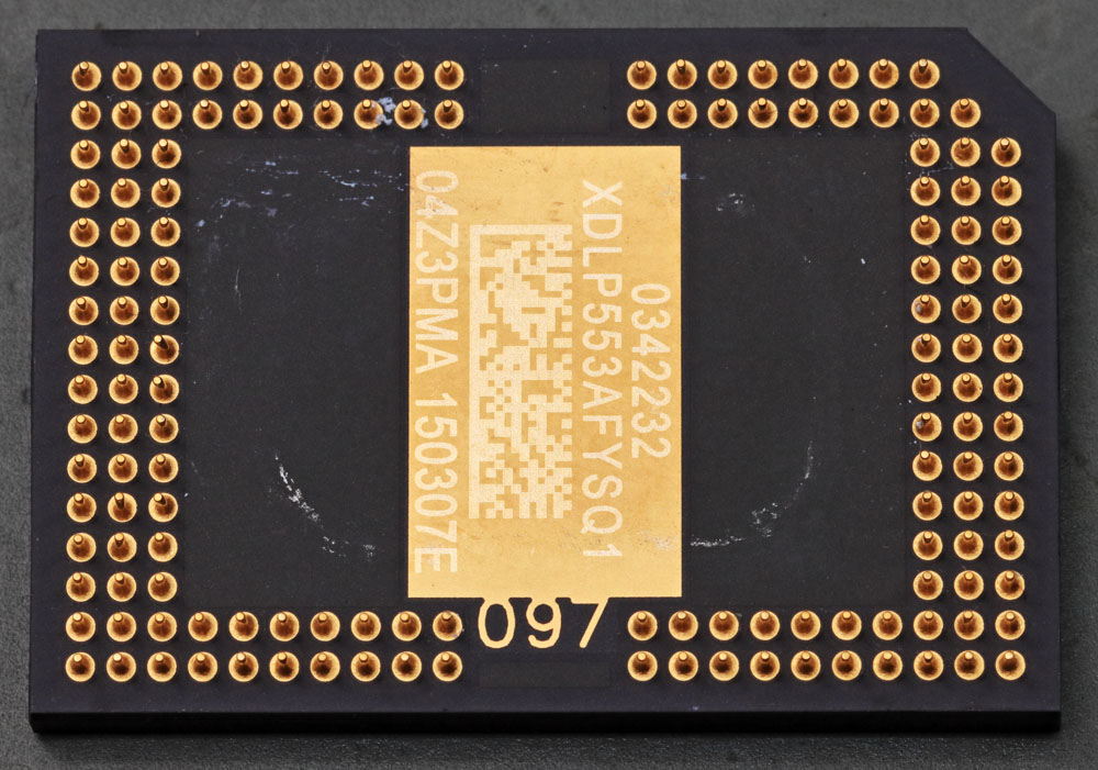
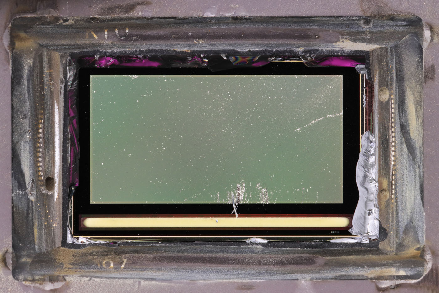
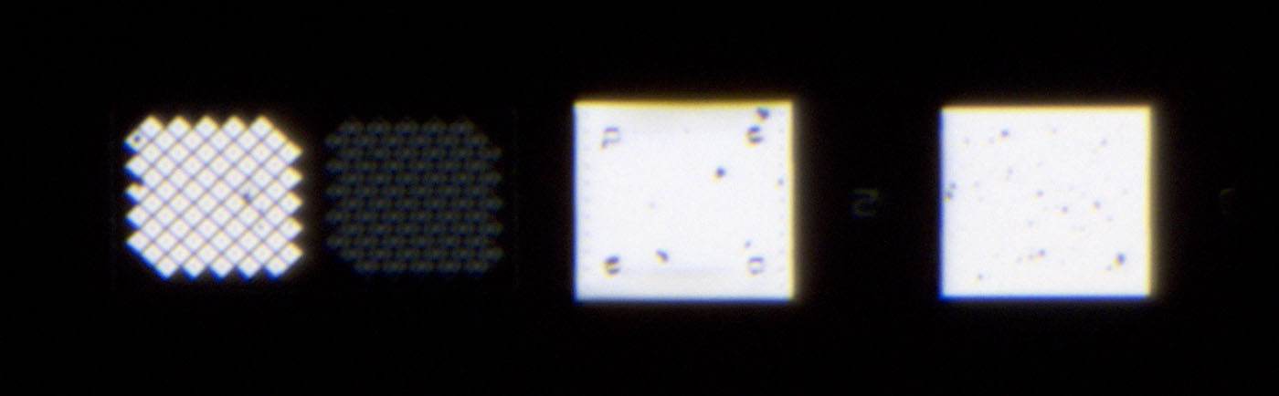
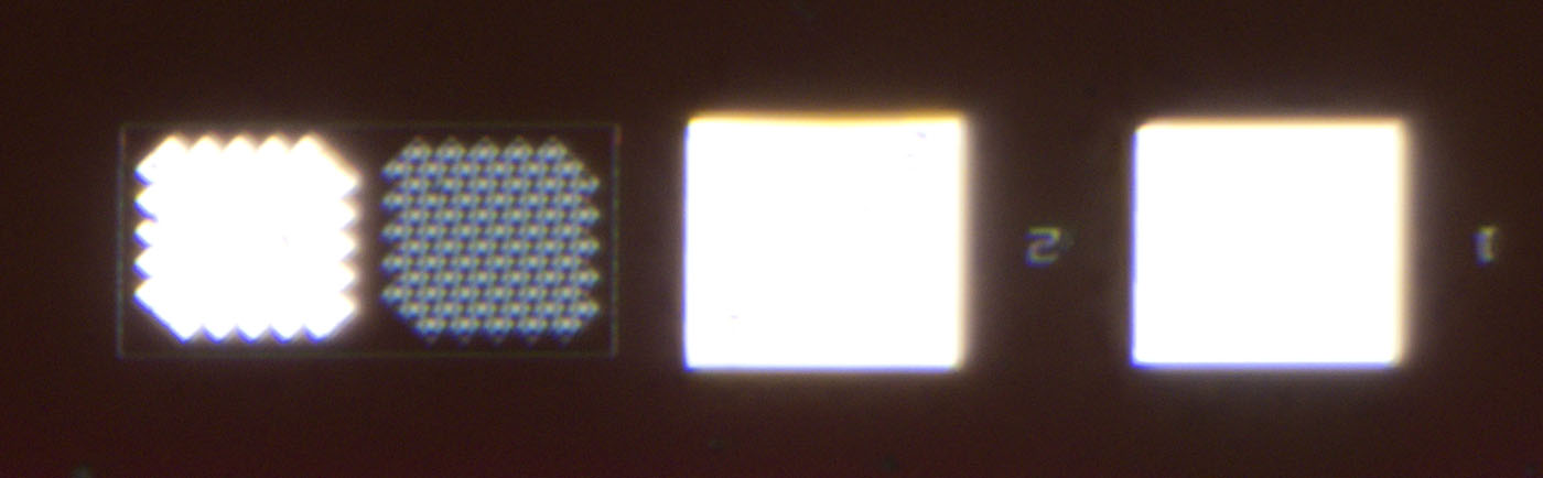
The module here is named XDLP553, which can not be found in the Texas Instruments documents. The individual variants of the DLP family don't seem to differ too much, though. Partially, the aperture within the window is arranged minimally differently. The DLP5530 is also subject to a special quality management.


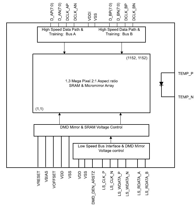
The datasheets show the basic structure of such a DLP module. As usual, the mirror array contains a SRAM placed directly under the mirrors, which contains the information how the individual pixels should be orientated. Two fast bus interfaces allow to write to this SRAM. A third bus is used to configure the DLP module, especially the voltages with which the mirrors are moved.


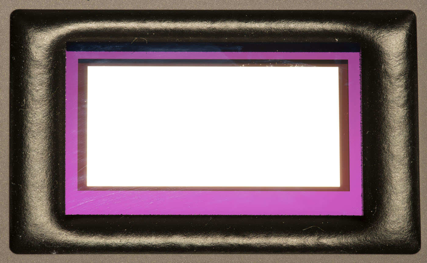
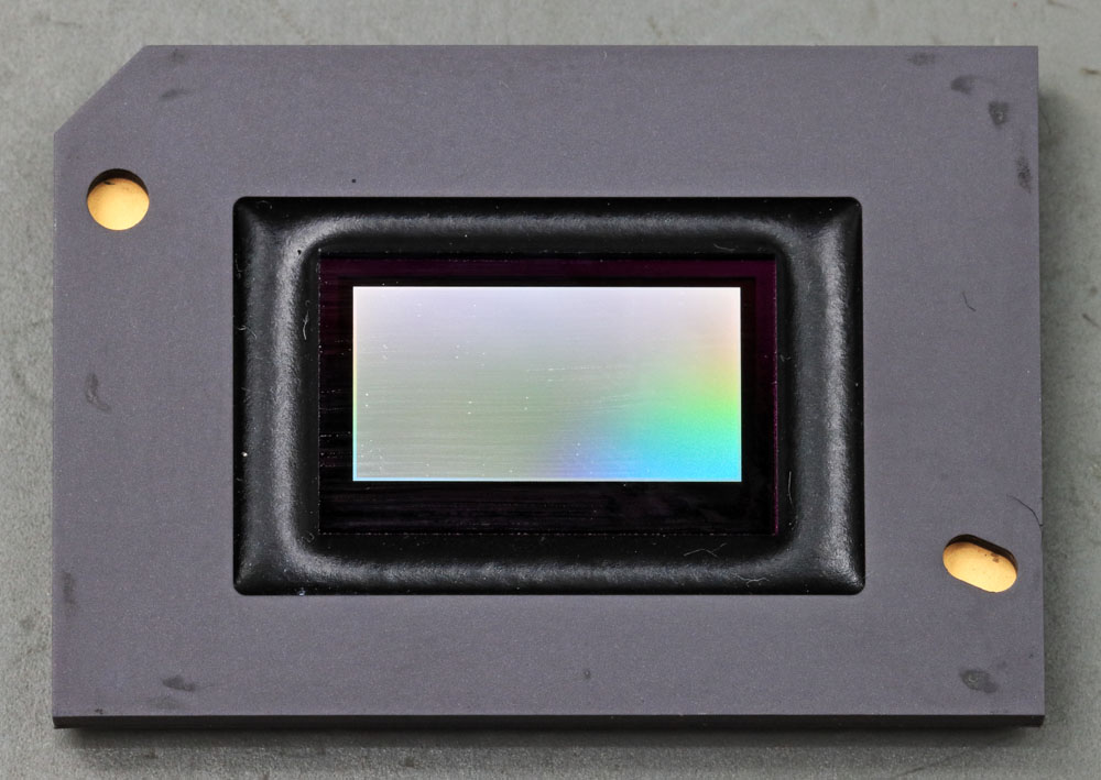
A window is glued into the ceramic housing. In the upper picture you can already see the thin inactive frame of the mirror array. In the lower picture, you can see that an aperture has been applied to the underside of the window. Parts of the integrated circuit around the mirror array are inside the aperture.


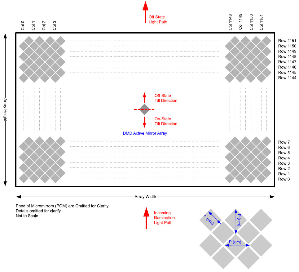
The datasheet shows the arrangement of the pixels in the DLP553x. Compared to the DMD1076, the individual mirrors are rotated by 45°. This arrangement is called a "diamond pixel array". Since the pixels partially overlap in this way, the effective resolution is just 1152 x 576 pixels, although the array consists of 1152 x 1152 mirrors. With the rotated array, the angles of incident and reflected light are more advantageous, allowing the optical system to be more compact.

The edge length of a mirror is given as 7,6µm, which apparently already includes the distance between the mirrors. The mirrors are thus significantly smaller than the mirrors of the DMD1076 (13,68µm). Around the usable mirror area there is a so-called "Pond of Micromirrors" (POM), a frame of inactive mirrors, which are not shown on the above sketch.


The POM frame is clearly visible. The necessity of this area also becomes clear. Functional mirrors can only be guaranteed inside the array due to the manufacturing process. For this reason, the mirrors are partially fixed in the POM frame. However, one must expect that individual elements are tilted.


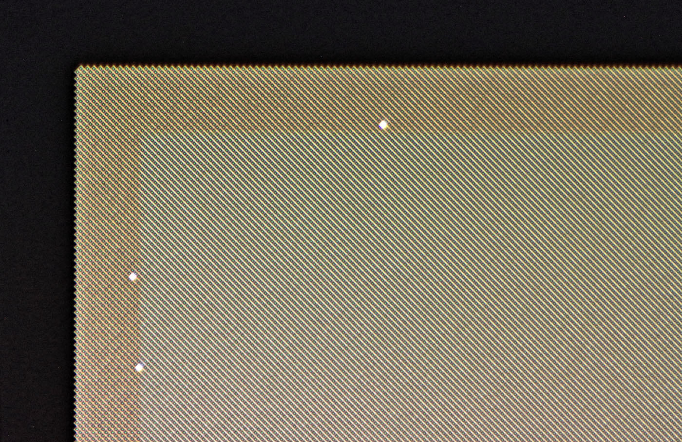
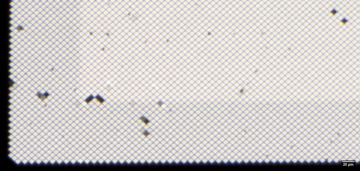
Depending on the incidence of light, the structures create very different patterns.


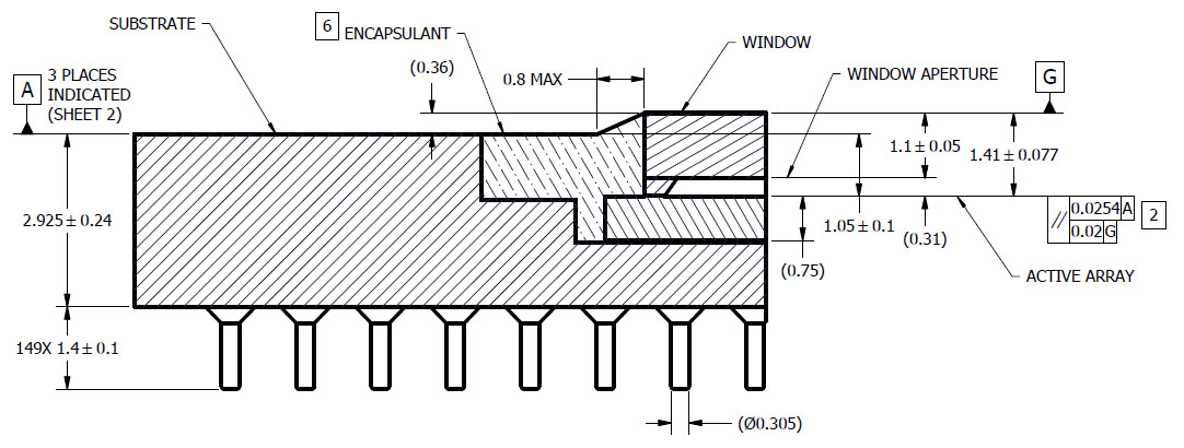
The datasheets show the constructional design of the case in section. The die is apparently slightly larger than the window. The potting in the frame provides the necessary tightness and mechanical stability.


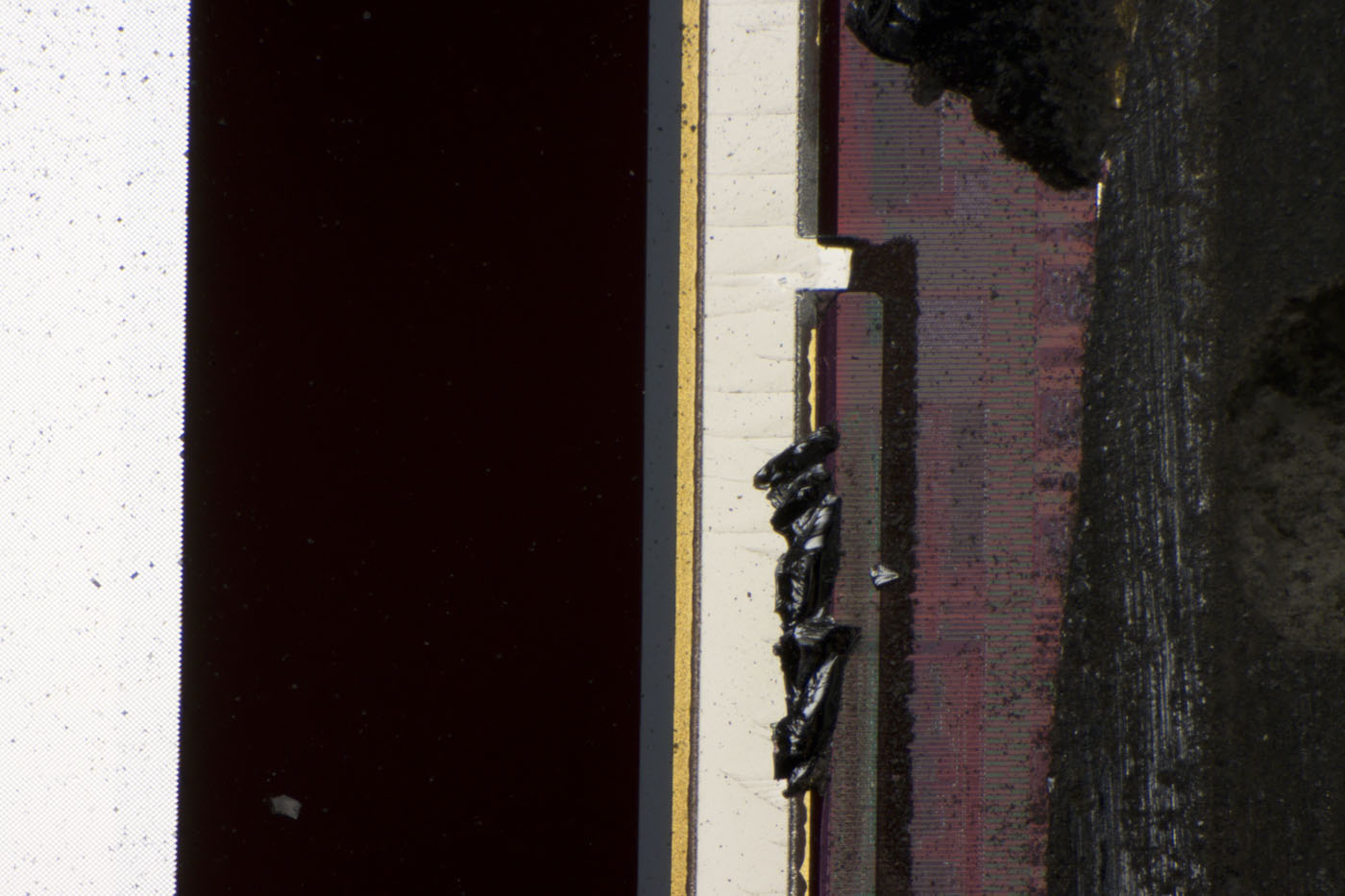
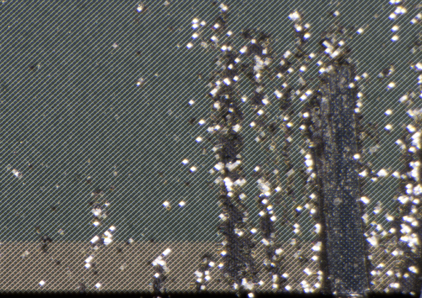
If you grind out the potting with a cutting disk, you can see some of the conductive paths that carry the potentials of the contacts to the die. In some places, you can even see the remains of the bondwires. In addition, some characters are exposed. The window still has to be broken out with some force, which damages the die a little.


In this picture the mirror array can still be seen on the left. To the right is a coating that appears black here. On the far right parts of the metal layer of the die can be seen.


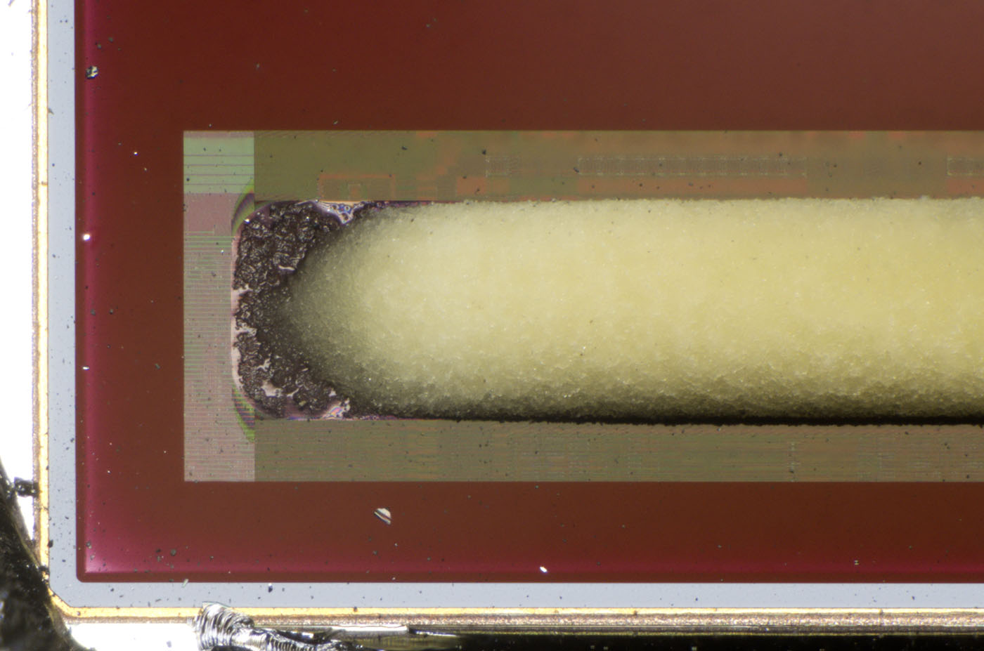
The purpose of the strip at the lower edge of the mirror matrix remains unclear. Shading of circuit parts could have been done with the coating that appears red here. It would be conceivable that it is some kind of drying agent or binder for problematic substances. However, this should actually no longer be necessary with modern manufacturing processes.
 :-//


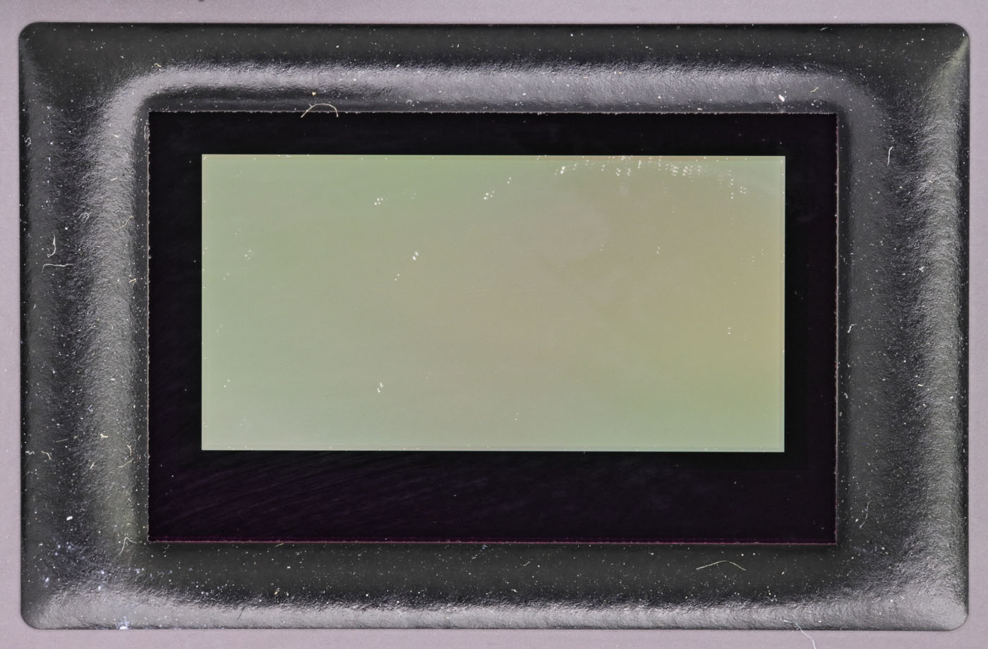
The mirror elements can just be resolved.


At the bottom edge there are some test structures. The left element contains some mirror elements. The area to the right of it could represent the underlying structures.


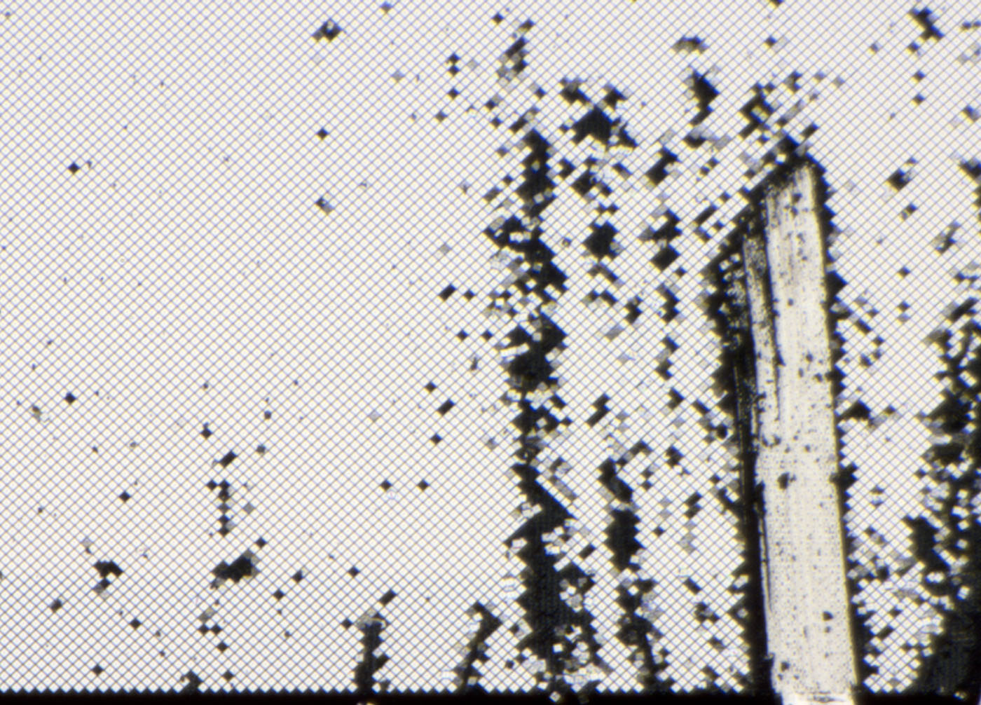
The damaged areas still allow a slightly different view on the mirror elements and the underlying structures.


https://www.richis-lab.de/MEMS_10.htm

 :-/O
 
The following users thanked this post: SeanB, RoGeorge, ROT

Online mikeselectricstuff

  • Super Contributor
  • ***
  • Posts: 13726
  • Country: gb
    • Mike's Electric Stuff
Re: MEMS - nice die pictures
« Reply #23 on: October 02, 2022, 11:08:26 am »
DLPs are cool but you really need an electron microscope
https://twitter.com/mikelectricstuf/status/1195940795821346816?lang=en-GB
Youtube channel:Taking wierd stuff apart. Very apart.
Mike's Electric Stuff: High voltage, vintage electronics etc.
Day Job: Mostly LEDs
 

Offline NoopyTopic starter

  • Super Contributor
  • ***
  • Posts: 1726
  • Country: de
    • Richis-Lab
Re: MEMS - nice die pictures
« Reply #24 on: October 02, 2022, 11:14:02 am »
DLPs are cool but you really need an electron microscope
https://twitter.com/mikelectricstuf/status/1195940795821346816?lang=en-GB

That's right. Unfortunately I have none. ^-^
It's a pity these electron microscopes are such expensive, big, bulky, complex... :-\


Share me

Digg  Facebook  SlashDot  Delicious  Technorati  Twitter  Google  Yahoo
Smf