Author Topic: Opamps - Die pictures  (Read 102492 times)

0 Members and 2 Guests are viewing this topic.

Offline NoopyTopic starter

  • Super Contributor
  • ***
  • Posts: 1731
  • Country: de
    • Richis-Lab
Re: Opamps - Die pictures
« Reply #300 on: July 14, 2022, 12:34:27 pm »


The LM310 is a voltage follower from National Semiconductor. We had already the LM310 built by Silicon General (https://www.richis-lab.de/Opamp08.htm) and the LM310 built by AMD (https://www.richis-lab.de/Opamp12.htm).


The edge length of the die is 1,2mm. Revisions of five masks are shown on the right edge. The numbers 110 refer to the LM110, the best bin of the voltage follower. The letters KB could be initials of a developer.

The design is similar to the AMD LM310 just the individual elements sometimes have a slightly different structure. In the Silicon General LM310 the bondpads and the circuit blocks are very similar, partly arranged in the same way, but bigger differences can be found.


In the lower left area of the die is an element that could be a test structure. The buildup and function remain unclear.  :-//


https://www.richis-lab.de/Opamp52.htm

 :-/O
 
The following users thanked this post: SeanB, xrunner, RoGeorge

Offline NoopyTopic starter

  • Super Contributor
  • ***
  • Posts: 1731
  • Country: de
    • Richis-Lab
Re: Opamps - Die pictures
« Reply #301 on: July 27, 2022, 03:27:01 am »


ST Microelectronics sells a µA741 variant under the designation UA741.


The data sheet contains a circuit diagram. You can immediately see that some lines are missing there.  ???

It is basically the same schematic as for the SGS ATES L141 (https://www.richis-lab.de/Opamp42.htm). This is hardly surprising, since ST Microelectronics emerged from SGS ATES, among others.


The design of the device is similar to the SGS ATES L141 (https://www.richis-lab.de/Opamp42.htm) and the Sescosem SFC2741 (https://www.richis-lab.de/Opamp07.htm). Both companies have been merged into ST Microelectronics. Apparently ST didn´t want to take over the µA741 variant of one of the two completely. Perhaps the design came from Thomson Semiconducteurs. This company was also integrated into ST Microelectronics.


The die shows the ST Microelectronics logo. In 1988 however the name of the company was still SGS Thomson. Probably the design was revised later and the ST logo was added in this context.


The character strings 2741.C and P728 are found on the edges. The latter is integrated into the metal layer in several deeper layers at a different location. This suggests that P728 is the internal designation for the design.


The revisions of eight masks are documented on the side. According to this the design was revised twice.


https://www.richis-lab.de/Opamp53.htm

 :-/O
 
The following users thanked this post: SeanB, doktor pyta, RoGeorge, capt bullshot

Offline NoopyTopic starter

  • Super Contributor
  • ***
  • Posts: 1731
  • Country: de
    • Richis-Lab
Re: Opamps - Die pictures
« Reply #302 on: August 07, 2022, 03:22:26 am »


I had a National Semiconductor LM709 built 1967 (https://www.richis-lab.de/Opamp20.htm). Now this one was built 1969.


The construction of the dies is very similar to the LM709 from 1967. The same elements can be found in the same circuitry. However, it is also clear that the arrangement was slightly revised and most likely a different manufacturing process was used.


https://www.richis-lab.de/Opamp54.htm

 :-/O
 
The following users thanked this post: SeanB, RoGeorge

Offline RoGeorge

  • Super Contributor
  • ***
  • Posts: 6202
  • Country: ro
Re: Opamps - Die pictures
« Reply #303 on: August 07, 2022, 08:00:10 am »
Great pics as always, thanks again!  :-+

More from the year 1969:  8)
https://www.historic-newspapers.com/blog/a-year-in-history-timeline-of-1969-events/
 
The following users thanked this post: Noopy

Offline NoopyTopic starter

  • Super Contributor
  • ***
  • Posts: 1731
  • Country: de
    • Richis-Lab
Re: Opamps - Die pictures
« Reply #304 on: August 13, 2022, 09:20:20 pm »


The HS-1135RH is a radiation hard operational amplifier originally developed by Harris Semiconductor and now produced by Intersil. The input resistance is 2MΩ. With a current consumption of 6,9mA the HS-1135RH offers a 3dB bandwidth of 350MHz and a maximum slewrate of 1,2kV/µs.


The HS-1135RH offers an adjustable limit for the output level. The datasheet shows the part of the circuit which does the high level clamping. Vh determines via the transistors Qn6, Qp6, Qp5 and Qn5 at which voltage current is diverted from the input of the output buffer. The opamp flips back to normal operation in less than a nanosecond.


The datasheet describes the die of the HS-1135RH in more detail. The upper metal layer is shown there too. Accordingly 89 transistors were integrated on an area of 1,50mm x 1,48mm. The process used for this is called UHF-1. A bonded wafer with dielectric isolation is used. The special structure prevents latchup due to free charges, which can be generated by radiation.


A description of the UHF-1 process can be found in the paper "UHF-1: A High Speed Complementary Bipolar Analog Process on SOI" published in the 1992 IEEE Bipolar Circuits and Technology Meeting. The process features two polysilicon layers and two metal layers. The high performance PNP transistors are particularly highlighted. The cutoff frequency of a NPN transistor is typically 9GHz, while the cutoff frequency of a PNP transistor is 5.5GHz. The gain factor is specified as 100 (NPN) and 40 (PNP).

The publication shows the structure of a PNP transistor, which has been recolored for better understanding. The basis is formed by two wafers which are connected by an insulating oxide layer. The upper wafer is first heavily p-doped, where it later functions as the collector lead (dark red).

The heavily doped and correspondingly low-resistance collector feed line is an important foundation for building PNP transistors with good specifications. In older DI processes it was not possible to integrate a deep heavily p-doping layer. According to the IEEE publication this was because such a p-dopant would have had to be introduced earlier in the process. The following process steps with their high temperatures would then lead to an unfavorable distribution of the doping.

In the UHF-1 process after building the collector feed line the epitaxial deposition of a weaker p-doped layer takes place which later represents the collector region (red). After this step the isolation of the active regions is completed. For this purpose a process creates deep trenches leading up to the isolation layer between the wafers. The trenches are lined with silicon oxide and filled with polysilicon.

The epitaxially applied collector layer is etched down a little around the active region of the transistor and is filled with a thick oxide layer. This reduces the base-collector capacitance and the base-substrate capacitance. The first polysilicon layer (yellow) contains an n-dopant which is allowed to diffuse into the underlying silicon as a base feed (dark blue). The actual base doping is then introduced into the active region (light blue). Due to its structure the transistor structure is self-aligned.

The second polysilicon layer (dark yellow) which is applied onto the base layer brings in the emitter doping (dark red). Apart from the inverted dopants, an NPN transistor has the same structure.

In addition to two metal layers (light green/dark green) the UHF-1 process also offers NiCr resistors that can be adjusted.


In the housing there is a small rectangular block next to the die which makes it easier to contact the bottom of the housing and thus the substrate. This contact is particularly important here as the substrate would otherwise be isolated and have an undefined potential.


At the very top of the die you can see a layer that is about 10µm high. This is probably the upper isolated layer of the wafer. In the case of OPA627 (https://www.richis-lab.de/Opamp22.htm) the insulated layer appeared to be 20µm high.


The circuit is still relatively clear.


In the upper right corner is the Harris Semiconductor logo. The number 93 probably stands for the year 1993, one year after the IEEE publication. 50749A03 could be the internal designation of the design. 21C, 22B, and 23B appear to be the mask designations and revisions for the two metal layers and the vias in between. SRJ and RJD could be abbreviations of the developers.


The various patterns on the upper edge of the die show that a large number of masks were used. The patterns make it possible to check the alignment of the masks.


The two test structures in the lower right corner of the dies certainly represent an NPN and a PNP transistor. Visually the structures can just be guessed. The many layers create an irregular surface structure that makes it difficult to recognize the relevant contours.


A large testpad is specially marked "NO BOND". From there a line leads around the circumference of the die to the negative supply potential. In the upper right corner, there are two orthogonally arranged resistors in this line. One can only speculate about the purpose of this long line. Perhaps the path is used when resistors are balanced.

In the lower left corner two resistors are integrated, which can be measured via testpads.


Even though the circuit is difficult to analyze in detail due to the two polysilicon and the two metal layers, it is quite easy to guess that the actual opamp is located in the middle of the die. It seems to be the classic setup with the circuit symmetrically arranged around the center. On the right the larger output stage transistors can be seen. A bit further to the left, two capacitors are integrated, which most likely realize the frequency compensation.


A large part of the area is taken up by a resistor array, which is most likely used for an offset adjustment. Traces of an adjustment process can be seen.

Surprisingly large protection structures are integrated at the signal inputs and at the clamping inputs.


https://www.richis-lab.de/Opamp55.htm

 :-/O
 
The following users thanked this post: SeanB, Vgkid, RoGeorge, ROT

Offline NoopyTopic starter

  • Super Contributor
  • ***
  • Posts: 1731
  • Country: de
    • Richis-Lab
Re: Opamps - Die pictures
« Reply #305 on: August 30, 2022, 10:06:11 am »


The LT1012 is a precision operational amplifier which is advertised in the datasheet as a better alternative to the OP07 (https://www.richis-lab.de/DAC07.htm#OP-07). Accordingly, the maximum offset voltage is 25µV with a maximum temperature drift of 0,6µV/°C. The bias current remains below 100pA. Between 0.1Hz and 10Hz, the noise voltage is a maximum of 0.5µVpp. A supply of +/-1.2V is sufficient for the LT1012. The current consumption is 500µA maximum. The cutoff frequency for this is just over 500kHz with a slew rate of 0.2V/µs maximum. With a feedforward compensation up to 10V/µs can be achieved.


To understand how the LT1012 works it is worth taking a closer look at the patent US4575685. Behind it are the almost legendary names Robert C. Dobkin, George Erdi and Carl T. Nelson.

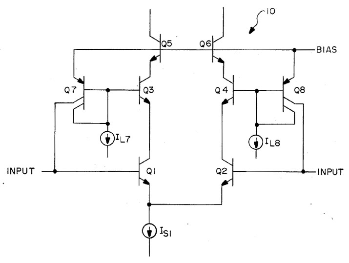
With the above picture the patent represents the state of the art to reduce the bias current of an operational amplifier. The collector lines of the input transistors Q1/Q2 contain the transistors Q3/Q4. If the transistors have the same structure, the base current of Q3/Q4 corresponds to the base current of Q1/Q2. Transistors Q7/Q8 mirror this current to the inputs where it compensates for the bias current.

In practice, however, leakage currents occur, indicated here by the current sinks IL7/IL8. As a result current flows away from the base of Q7 and Q8 which negatively affects the compensation current. The typical lateral PNP transistors have a large contact area between the base region and the substrate or the insulation surfaces. Relevant leakage currents occur there especially at high temperatures. Another disadvantage of the above circuit is that it is influenced by the common mode voltage at the inputs. Nevertheless it is quite sufficient for many operational amplifiers. However, if you want to work with very small input currents, you have to improve the bias compensation.


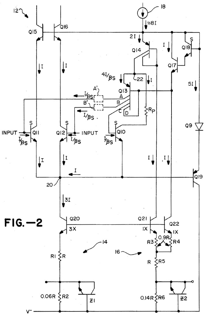
Patent US4575685 deals with a circuit that compensates the bias currents more precisely, but is also considerably more complex. The transistors marked with an S are so-called "super-beta transistors". These transistors offer a very high gain factor in the range between 1.000 and 10.000. In addition, they can be manufactured with very similar electrical characteristics, which is particularly helpful here.

The additional current sink Q21 determines with the current mirror Q14 that the same current I flows in direction Q13/Q10 as to each of the input transistors Q11/Q12. The interconnection of Q13/Q10/Rp ensures that a base current is established at Q10 so that current I can flow out via Rp. Q13 does not form a current mirror in the classical sense. Q14 drives current through the emitter of Q13 until enough current flows through its collector C to drive Q10 to the point where current I flows through its collector. The base current of the super-beta transistor is so small that it can be neglected.

Q13 now transfers currents to the inputs via its collectors A and B which correspond to the base current of Q10. Since Q10 has the same structure as the input transistors Q11/Q12 and also conducts current I, the base currents of all three transistors are equal and the currents of Q13 can compensate for the bias currents at the inputs. The collector D is not needed and is just present so that the transistor can be constructed symmetrically. As a lateral PNP transistor Q13 suffers from the same leakage currents as the PNP transistor of the first circuit but here they are fed by Q17 and thus do not affect the compensation of the bias currents.

The patent specifically notes the importance of current mirror Q14. If the voltage at the inputs reduces faster than 0,1V/us the capacitance at the base of Q10 would be sufficient for Q10 to take most of the current from Q20. The operating point of Q11/Q12 would shift due to the lack of current and the transfer characteristics would deteriorate. The capacitance at the base is typically no more than 20fF. However, the base current discharging this capacitor is also just 0,5nA to 2nA due to the super beta transistor. Since Q14 limits the current through Q10 to the value I Q10 not only is prevented from taking current from the input transistors Q11/Q12. Q10 thereby saturates which increases the base current and quickly discharges the parasitic capacitance there. This ensures that when the voltage at the inputs changes rapidly the bias current does not fluctuate.

In order for transistors Q11/Q12/Q10 to behave as equally as possible their collector-base voltages should be equal. It is also advantageous if the voltage is small and independent of the common mode voltage at the input. The collector-base voltage of Q11 is determined by the base-emitter voltages of Q19/Q9/Q15/Q11. According to the patent the different current values and transistors provide a collector-base voltage in the range of 0.1-0.2V.
The collector-base voltage of Q10 is defined by the path Q15/Q16/Q18/Q17/Q13/Rp. The same voltages are present at Q10 and Q11 if the base-emitter voltage of Q13 has the same value as the sum of the base-emitter voltage of Q18 and the voltage drop across Rp. Although these are very different elements, the patent states that this requirement is satisfied relatively well even at different temperatures.

The surrounding current sources and sinks must, of course, be constructed so that the necessary currents are established. Below the differential amplifier these are not 2I but 3I due to the additional transistor Q10. According to the patent the same current does not necessarily have to flow in the right-hand branches Q21/Q22 as in the input transistors, but the currents must be constantly proportional to each other. The ratio, which also affects the base currents, can then be corrected via the resistors A' and B'.

The Z-diodes Z1 and Z2 represent fuses that can be triggered in production and make it possible to adjust the current ratio of Q20 to Q21/Q22 accordingly. Thus the strength of the bias current compensation can be adjusted.


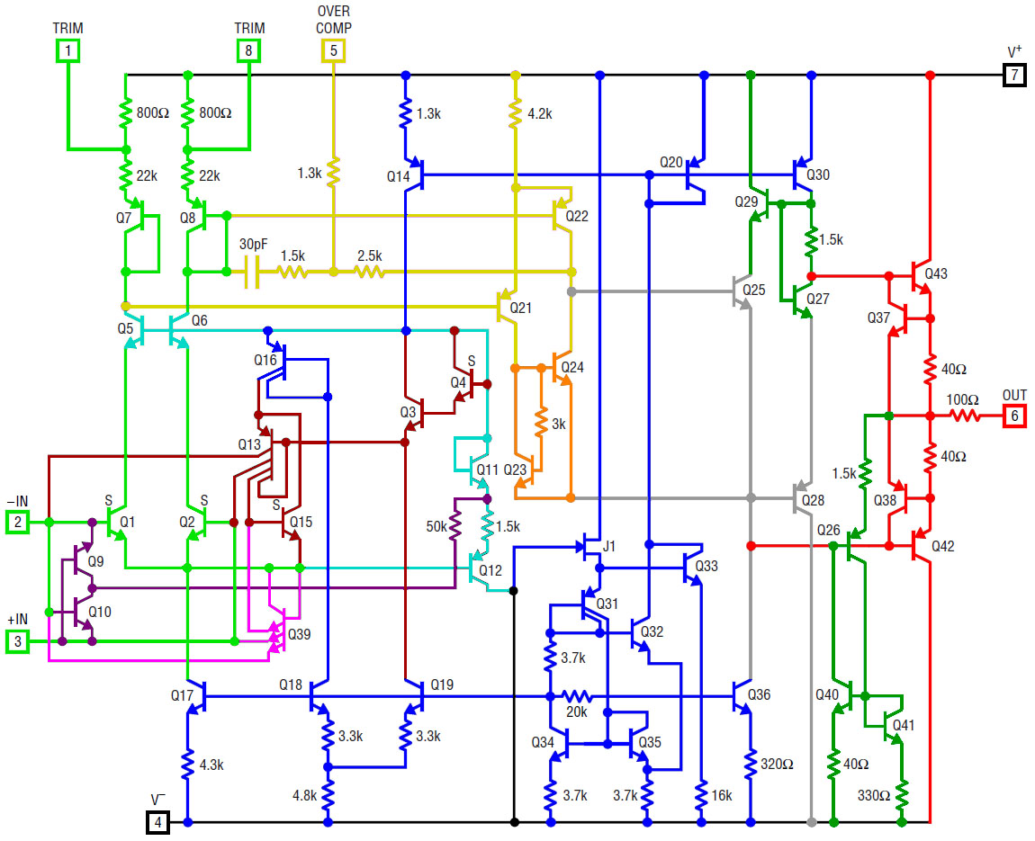
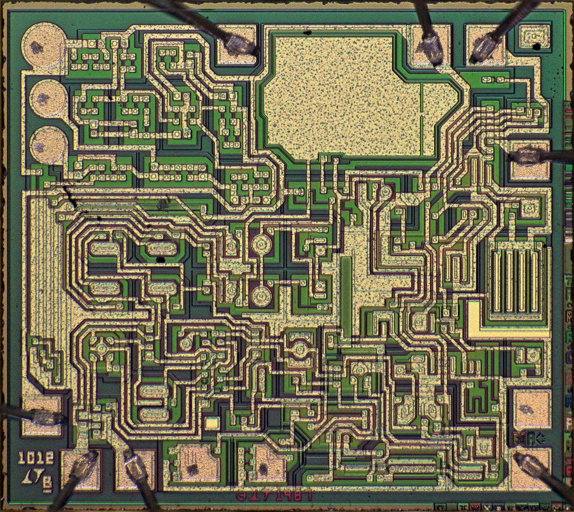
The datasheet contains a circuit diagram, which is much easier to understand with the above background information. As usual the biasing of the different circuit parts is done by a series of current mirrors (blue). The generation of the reference current is surprisingly complex.

The input transistors in the differential amplifier (light green) are super beta transistors. The very high current gain factor is of course extremely advantageous for the input transistors. At the collector resistors the trim pins are connected, which allow an adjustment of the offset from outside the package.

The cyan circuit, as described in the patent above, ensures that the collector-base voltage of the input transistors Q1/Q2 remains constant. The dark red circuit part maps the compensation of the bias current, also described in the above patent.

In addition to the bias current compensation, the differential amplifier features Q9/Q10 (purple) and Q39 (pink). Q9 and Q10 serve as clamping diodes, limiting the input voltage between -IN and +IN. The purpose of the connection to the cyan circuit remains unclear. Current can flow across this connection only if an input potential becomes lower than the emitter potential of the input transistors.
Q29 gives you three diodes, which apparently should accelerate the clearing of the free charge carriers in the super beta transistors. What is otherwise more relevant for power transistors could also be helpful here due to the high gain factors.

The voltage amplifier (yellow) is based on transistor Q22. Via pin 5 the frequency compensation can be extended externally. Q24/Q24 (orange) generate the voltage drop, which provides some quiescent current in the output stage. Q21 is driven inventoried to Q22 and can take over its current, which makes the highside of the output stage activate faster.

Q25 and Q28 represent the drivers of the power stage (gray). If the voltage amplifier stage supplies more current Q25 conducts more current and the level of Q28 decreases. This means that Q42, the lowside transistor of the output stage, is driven less. At the same time, more current flows from Q30 into the highside transistor of the power amplifier stage (Q43) and drives it harder.
If the voltage amplifier stage reduces the current, the excitation of Q25 decreases, more current flows out of Q42, and the output of the opamp swings toward the negative supply potential. At the same time Q28 conducts more current and reduces the excitation of the highside transistor.

The complementary output stage (red) is equipped with an overcurrent protection circuit (Q37/Q38). The 100Ω resistor at the output improves the behavior with capacitive loads.

Between driver and output stage there are further protection circuits (dark green). Q26 becomes conductive when the output has a high potential and the lowside transistor of the output stage is driven strongly. As a consequence, Q41 and Q40 become conductive, which reduces the output level. This ensures that transistor Q42 is not loaded beyond its SOA range.
Q27 reacts similarly. The output potential is applied to its emitter via Q28 and Q42. If this potential is very low and a high current flows across the 1,5kΩ resistor at the same time, Q27 sinks the base current of the highside transistor. Q29 simultaneously reduces the current flow through Q25, which means that the hihgside transistor is driven even less hard.


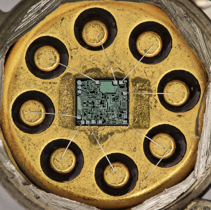
One bondwire connects the pin of the negative supply to the housing.


The Die ist 1,8mm x 1,6mm.


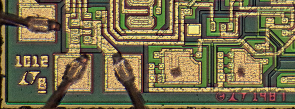
The design dates from 1987. The B could indicate a second revision.  :-//


The milling path contains the revisions of nine masks and some patterns that allow to check the alignment of the masks against each other.

The circuit includes several Zener fuses. A metal fuse is integrated between the negative supply potential and a testpad which does not interfere with the circuit. Presumably it was triggered during alignment, perhaps to indicate the quality level.


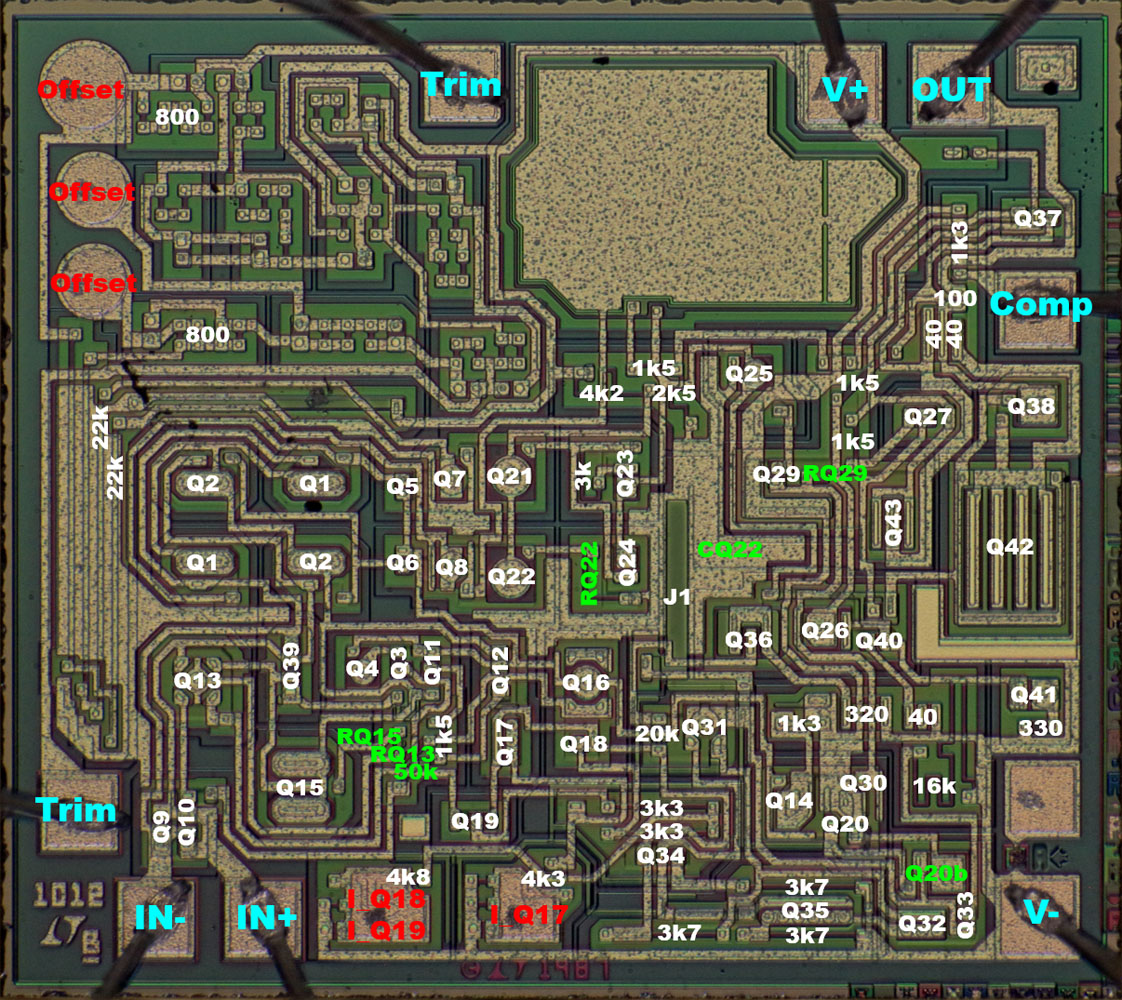
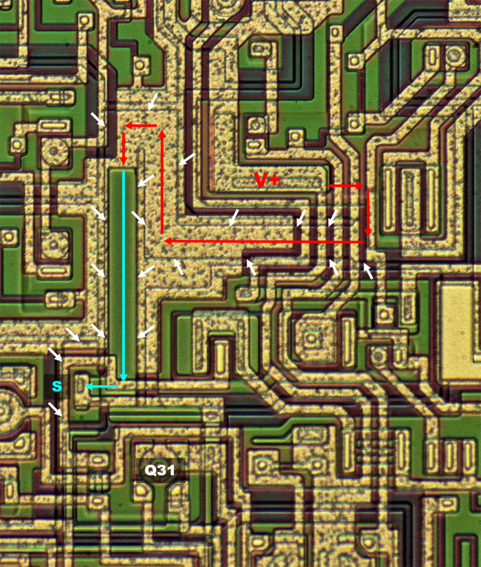
Most of the elements are easy to identify on the die. The round testpads in the upper left corner allow to adjust the offset of the input stage. The rectangular testpads on the bottom edge give you the opportunity to adjust the bias current compensation.

The input stage is arranged to have a low temperature drift. The input transistors Q1/Q2 are doubled up and arranged crosswise in the center. On the far left they keep a large distance from the output stage on the right edge, where the most power dissipation occurs. Even the collector resistors are integrated in the center at the left edge. To the right the electrically following transistors up to the voltage amplifier are arranged around the middle of the die.

The circuit corresponds mostly to the schematic in the datasheet, but there are some minor differences (light green). The pinch resistor RQ15 is found at the collector of Q15, which is the resistor referred to as Rp in the patent specification.
The resistor RQ13 is located between Q13 and Q16, this seems to be just an undercrossing of a line. At this point, a resistor has little effect on the circuit.
The 50kΩ resistor connected at one end to the clamping diodes at the input does not lead to the upper but to the lower end of the 1,5kΩ resistor above Q12.

In the collector of Q22 there is the resistor RQ22. It seems that here one wanted to create a symmetry to the second transistor of the voltage amplifier stage. Behind this resistor the line is formed into a relatively large area, which represents some capacitance to the negative supply potential (CQ22).

At the base of Q29 there is the resistor strip RQ29, but this probably serves just as an undercrossing.

Also not shown in the schematic is the transistor Q20b, which is a base current compensator for transistor Q20, which operates as a current mirror.


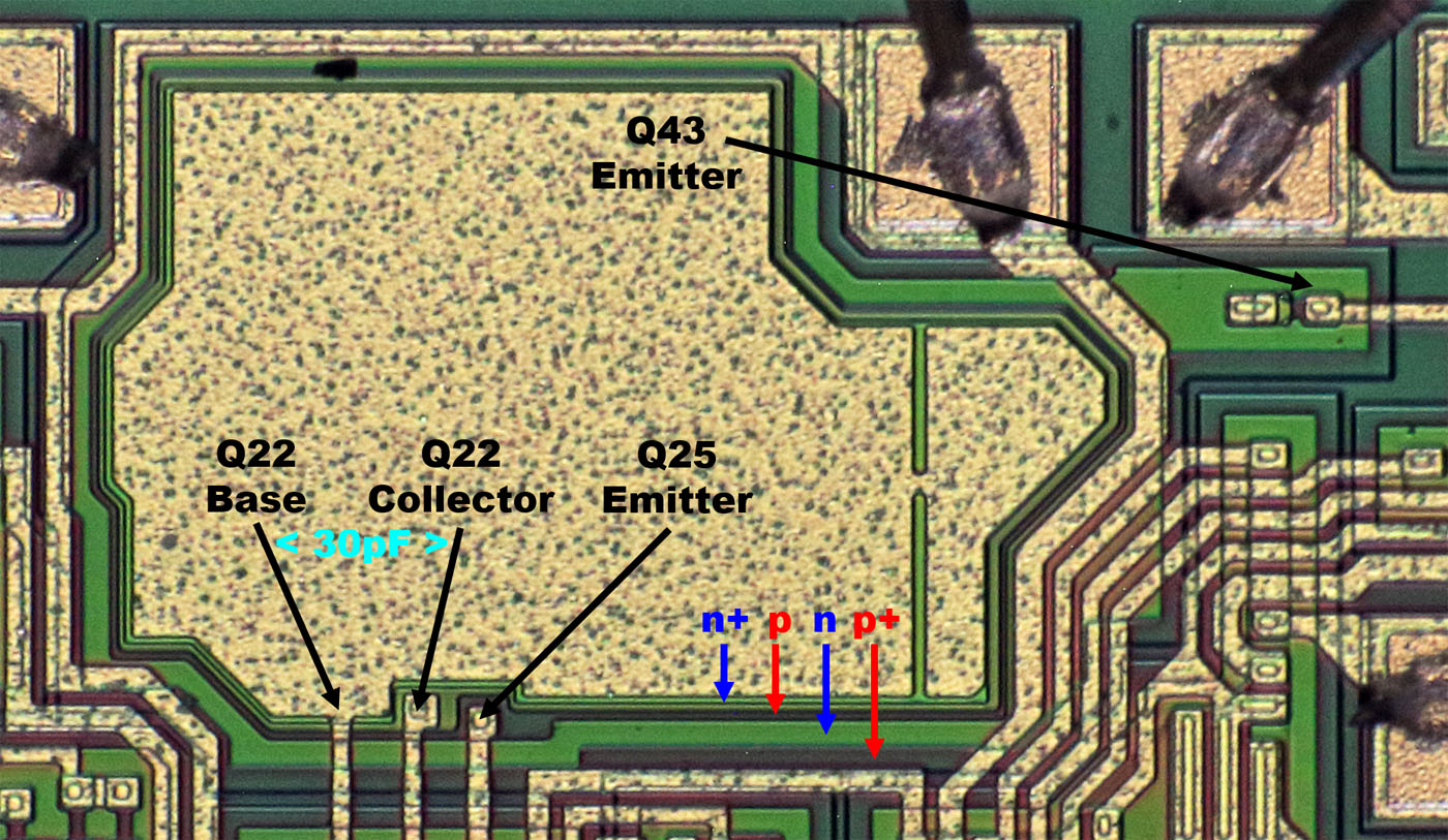
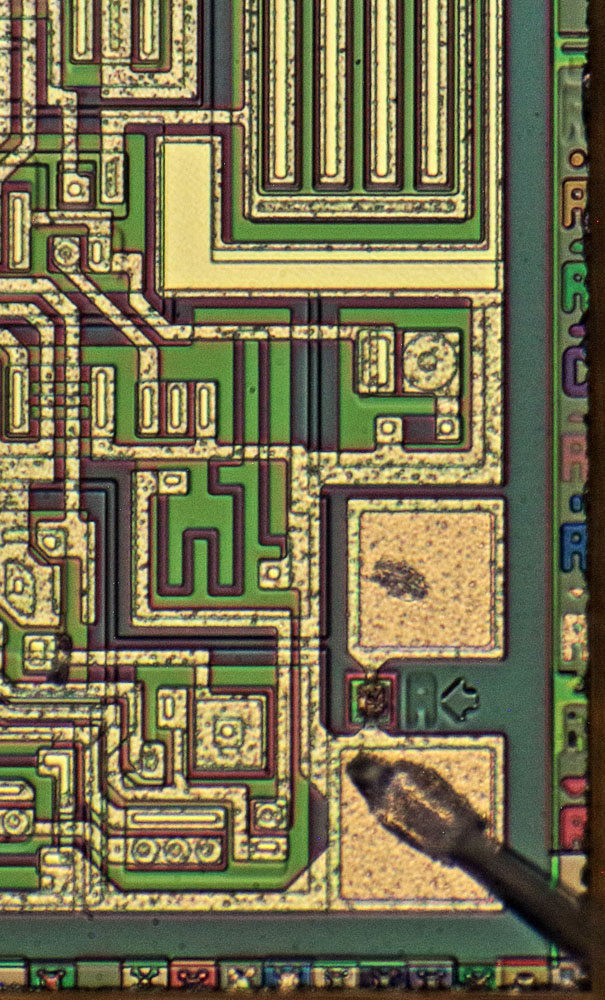
On closer inspection the large capacitor has a somewhat more complex structure than shown in the datasheet. The capacitance of 30pF is set between the metal layer and the green n-doped layer underneath. The edge surrounding the metal layer shows that there is a thinner oxide layer under the metal layer, which increases the capacitance. The metal surface has an area that can be separated via a thin contact. This makes it easier to adjust the capacitance if necessary.

The dark p-doped surface on which the capacitor is placed is connected to the emitter of Q25. Electrically adding capacitance to this node seems to have no effect on the circuit. For a safe isolation of the capacitor one could have simply connected the area to the negative supply. Probably this measure was taken to keep the parasitic capacitance to the substrate away from the voltage amplifier stage. Since it is a pn junction, this capacitance would fluctuate with the signal level and could thus cause distortion. The potential of the emitter of Q25, on the other hand, is constantly one base-emitter voltage below the potential of the collector of Q22.

The inner, green layer of the capacitor is most likely the emitter doping. It is embedded in the dark layer which is then represented by the base doping. Surrounding the whole structure is a green frame, most likely the collector doping, and finally the dark isolation frame. On the right side of the picture, the emitter potential of Q43 contacts the capacitor area. The lead is connected to a strip of the base material. Thus the collector area should be at about the same potential as the base area under the capacitor and the 30pF capacitor is thus maximally well shielded. The metal surface to the left of the Q43 contact seems to connect the collector surface to the buried collector.


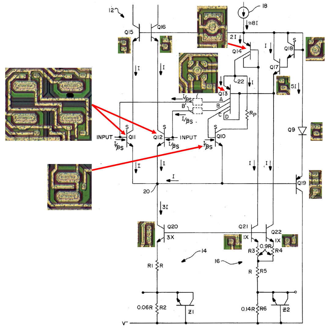
If one inserts the transistors in the correct size ratio into the circuit diagram of the patent an interesting picture emerges. The current sinks Q20/Q21/Q22 are constructed in the specified ratio of 3:1:1. The same current density ensures maximum synchronism.

The doubled super beta transistors Q11/Q12 at the inputs are relatively large. To ensure the same current density in transistor Q10 it has two emitter areas. The super beta transistor Q18 is smaller but still large for an NPN transistor. The other NPN transistors Q15/Q16/Q17/Q9 are rather inconspicuous.

The symmetrical structure of the PNP transistor Q13 can be seen well. One of the collectors is led back to the base. The PNP transistor Q14 has to carry more current and is designed accordingly larger. The upper metal surface directly connects the upper collector surface with the base surface. The PNP transistor Q19 has an unusual design. Two p-doped areas, one slightly longer, are located in an n-doped area which carries the base potential.


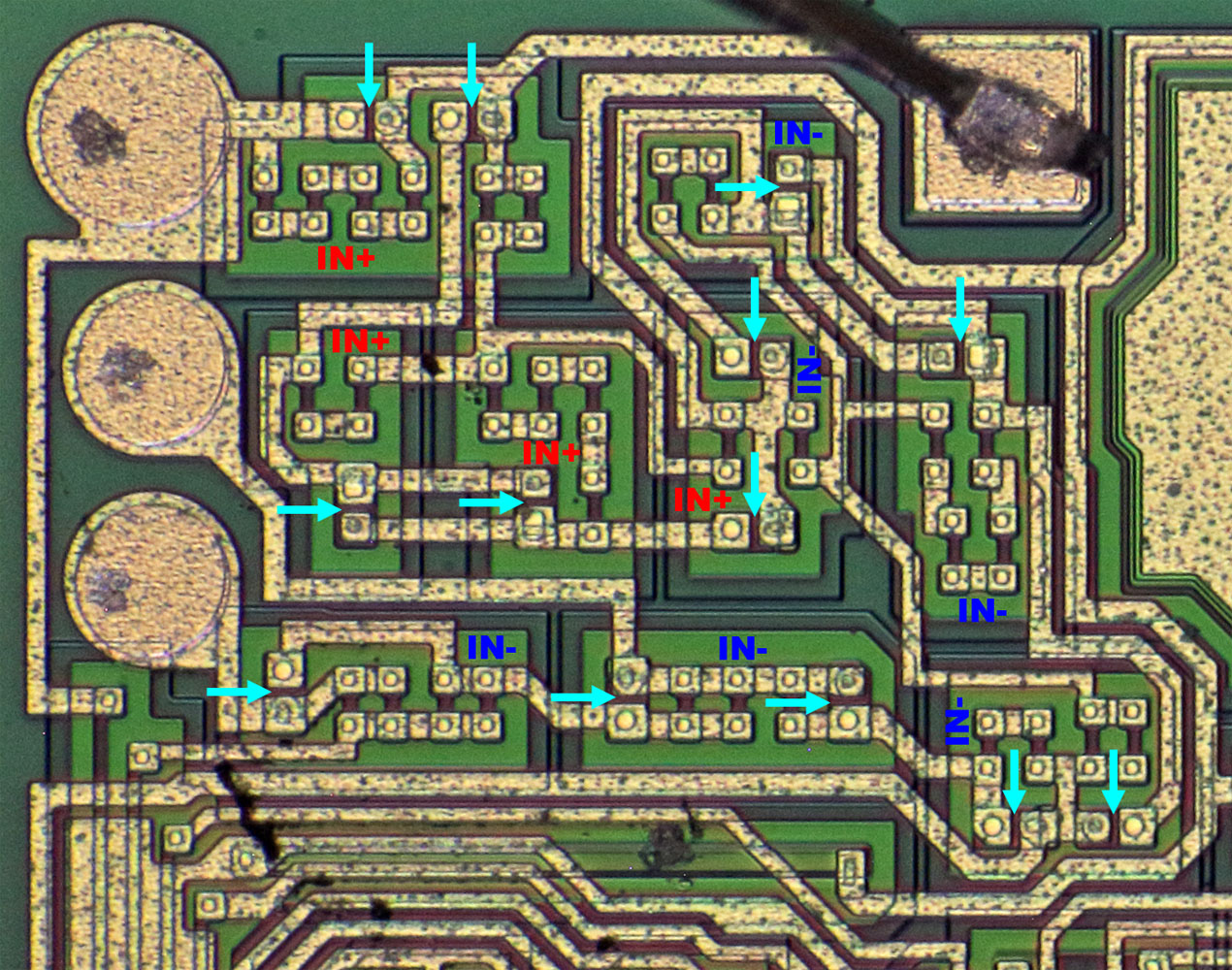
The two 800Ω resistors above the large collector resistors are amazingly complex. The input offset can be adjusted externally by the corresponding pins. In addition the testpads can be used to configure the resistors during manufacture.

Although there are just three testpads a total of 13 Zener fuses can be triggered. We have seen these series connected Zener fuses that can be triggered selectively in the LT1013 too (https://www.richis-lab.de/Opamp26.htm). In the LT1012 this technique has been used even more excessively. This reduces the need for testpads which saves a lot of space.


The JFET generating the reference current for the current sinks and sources can only be guessed at a very close look. A strip leads from the positive supply potential over a relatively long distance. The edges of the stripe show up through the metal layer (white). Initially the material appears dark (red). Here the collector doping seems to be completely covered by the base doping. This would result in an n-doped channel with a p-doped cladding. On the last part of the strip (cyan) is a green layer, presumably the collector doping, which appears to be contacted away from the contact to the buried collector feed line. The purpose of this division remains open.  :-//


https://www.richis-lab.de/Opamp56.htm

 :-/O
 
The following users thanked this post: SeanB, RoGeorge, floobydust, capt bullshot, magic, ROT

Offline NoopyTopic starter

  • Super Contributor
  • ***
  • Posts: 1731
  • Country: de
    • Richis-Lab
Re: Opamps - Die pictures
« Reply #306 on: September 04, 2022, 06:01:46 pm »


The OP07 was developed by Precision Monolithics and offers a very low offset voltage. The OP07C represented the worst bin at the time with a maximum offset voltage of 250µV, a longterm drift of typically 0,4µV/month (2,0µV/month maximum) and a voltage noise of typically 0,38µVpp (0,1Hz-10Hz; 0,65µVpp maximum). The OP07A variant was the best bin and offers a maximum offset voltage of just 45µV, a typical longterm drift of 0,2µV/month (1,0µV/month maximum) and a voltage noise of 0,35µVpp (0,6µVpp maximum). The operating voltage can be selected between +/-3V and +/-18V. The cutoff frequency is typically 0,6MHz, and the slewrate is specified at 0,17V/µs.


The OP07 was advertised by PMI as early as 1976 in Electronic Design 16. Analog Devices produces this operational amplifier still today.


The new datasheet from Analog Devices shows the same circuit diagram as the old datasheets from PMI. The differential amplifier at the input (blue) is equipped with diodes that limit the input voltage (Q21-Q24). The collector resistors contain taps connected to the offset pins. R2A and R2B are tuned during fabrication.

OP07 includes a bias compensation (green). As described with the LT1012 transistors Q3/Q4 carry the same currents as input transistors Q1/Q2 and accordingly draw similar base currents. Q5/Q7 and Q6/Q8 copy these currents and feed them into the inputs where they compensate the bias.

Between the input amplifier (blue) and the voltage amplifier stage (red) emitter followers are integrated as a buffer (purple). The signals are still differentially routed in this area. The voltage amplifier stage works against a current mirror (Q13/Q14). The frequency compensation is relatively complex (cyan). C2 represents the actual frequency compensation. C1 attenuates high frequencies in the uncompensated path. C3 implements feedforward compensation that bypasses the PNP transistors at high frequencies. According to "Precision Monolithics Linear & Conversion I.C. Products" from 1977 a total of 210pF was integrated into the OP07.

A driver stage (yellow) controls the push-pull output stage (dark red) which is permanently short-circuit proof according to the datasheet. The schematic doesn´t show any shortcircuit protection, but on the die a corresponding circuit can be seen. The gray circuit provides a certain voltage drop between Q19 and Q20 and thus generates the necessary quiescent current.


The manual "Precision Monolithics Linear & Conversion I.C. Products" mentioned above shows the residual bias current and its variation over temperature. For even lower bias currents, more complex circuits are required, such as those integrated in the LT1012 (https://www.richis-lab.de/Opamp56.htm).


The housing is directly connected to the negative supply potential.


The dimensions of the dies are 2,55mm x 1,35mm.


"Precision Monolithics Linear & Conversion I.C. Products" shows the arrangement and function of the individual bondpads. The NC bondpads are used to adjust the offset voltage.


On the die you will find the characters OP.07.Z. PMI marked revisions by counting up from Z to A. This means that the present design is the first one. In the AD1139, on the other hand, the revision U can be found (https://www.richis-lab.de/DAC07.htm#OP-07). The year 1986 is shown on this die, so it is about 10 years older.


The differences between revision Z and revision U are minimal and seem to be functionally irrelevant for the most part. Just resistor R7 in the driver of the power amplifier seems to have been lengthened somewhat.


"Precision Monolithics Linear & Conversion I.C. Products" shows how to tune the offset voltage in the input stage. Four testpads allow to trigger four Zener fuses which subsequently bridge the collector resistors R2C, R2D, R2E or R2F. The resistor ratio defines the offset voltage.


Several small resistors are integrated around the four testpads on the die. The somewhat larger areas containing the Zener fuses can be seen too.


The exact structure of a Zener fuse can also be found in the "Precision Monolithics Linear & Conversion I.C. Products". It is a Zener diode, more precisely the base-emitter path of a NPN transistor. When the Zener fuse is triggered the structure is destroyed and shorted. The shortcircuit is formed by the melting of the surrounding metal into the intervening base-emitter path.


https://www.richis-lab.de/Opamp57.htm

 :-+
 
The following users thanked this post: SeanB, RoGeorge, magic

Offline iMo

  • Super Contributor
  • ***
  • Posts: 4780
  • Country: pm
  • It's important to try new things..
Re: Opamps - Die pictures
« Reply #307 on: September 04, 2022, 06:31:31 pm »
FYI - I own several PMI OP07AY in DIL14 ceramic package, there is a picture I published here (I will find it).
Based on an old PMI datasheet I downloaded that AY version was with the best params (I will find the DS).
PS: the 1976 PMI OP07 datasheet
« Last Edit: September 04, 2022, 06:50:03 pm by imo »
 

Offline NoopyTopic starter

  • Super Contributor
  • ***
  • Posts: 1731
  • Country: de
    • Richis-Lab
Re: Opamps - Die pictures
« Reply #308 on: September 04, 2022, 06:57:29 pm »
FYI - I own several PMI OP07AY in DIL14 ceramic package, there is a picture I published here (I will find it).
Based on an old PMI datasheet I downloaded that AY version was with the best params (I will find the DS).
PS: the 1976 PMI OP07 datasheet

Well the AY is the A in the DIL-Package with a higher temperature rating. So the AY is a little better. But the A is the best bin in the TO-99 package.
So you are right and I´m right too.  ;) ;D
 
The following users thanked this post: iMo

Offline magic

  • Super Contributor
  • ***
  • Posts: 6778
  • Country: pl
Re: Opamps - Die pictures
« Reply #309 on: September 04, 2022, 07:02:25 pm »
There is a second level of cascode over the input stage, not shown in the datasheet, which ensures that the first level cascode transistors have the same collector-emitter voltage as the input pair. I suppose it improves base current cancellation accuracy over common mode input range and increases input impedance. OP-07 bias cancellation is exactly the "prior art" circuit shown in that LT1012 patent. (Good find, BTW, I never understood why LT1012 is so weird).

There is C4 in OP-07, going between the right-hand ends of C2 and C3. It implements Miller compensation of that internal 2-stage opamp-inside-opamp.

Complete schematic can be found in old datasheets from TI. Very ugly like most TI schematics and has some small errors in the output stage, but still quite helpful.
 
The following users thanked this post: Noopy

Offline iMo

  • Super Contributor
  • ***
  • Posts: 4780
  • Country: pm
  • It's important to try new things..
Re: Opamps - Die pictures
« Reply #310 on: September 04, 2022, 07:04:25 pm »
Btw I've been using one of them actively in my 2xLT1021-10 ref source as the buffer. I will desolder it soon as the ref source with the epoxy LT1021 is a crap (large hysteresis).
When it gets damaged I will send it to you for autopsy.. :D
« Last Edit: September 04, 2022, 07:10:55 pm by imo »
 
The following users thanked this post: Noopy

Offline NoopyTopic starter

  • Super Contributor
  • ***
  • Posts: 1731
  • Country: de
    • Richis-Lab
Re: Opamps - Die pictures
« Reply #311 on: September 04, 2022, 07:10:39 pm »
There is a second level of cascode over the input stage, not shown in the datasheet, which ensures that the first level cascode transistors have the same collector-emitter voltage as the input pair. I suppose it improves base current cancellation accuracy over common mode input range and increases input impedance. OP-07 bias cancellation is exactly the "prior art" circuit shown in that LT1012 patent. (Good find, BTW, I never understood why LT1012 is so weird).

There is C4 in OP-07, going between the right-hand ends of C2 and C3. It implements Miller compensation of that internal 2-stage opamp-inside-opamp.

Complete schematic can be found in old datasheets from TI. Very ugly like most TI schematics and has some small errors in the output stage, but still quite helpful.

You are right.  :-+
I didn´t check all the components but it was clear that there is some more than shown in the datasheet.
Can you give me a link to the old TI datasheet? I can´t find it. The newer one is no help.

Offline magic

  • Super Contributor
  • ***
  • Posts: 6778
  • Country: pl
Re: Opamps - Die pictures
« Reply #312 on: September 04, 2022, 07:19:36 pm »
It's very helpful if you want to know more about TI's version of LM741 ;D

This one is good.
http://www.elenota.pl/datasheet-pdf/49486/Texas-Instruments/OP07C

Even die image is included and it's authentic.
https://www.eevblog.com/forum/projects/decapping-ics-for-investigation/msg1118381/#msg1118381
For some reason, it looks like more area is devoted to capacitors :-//

Generally, to find old TI datasheets, look at the TI literature number on the first page, like SLOS099G.
Then change the letter at the end, say SLOS099B, and just search for it.
 
The following users thanked this post: Noopy

Offline NoopyTopic starter

  • Super Contributor
  • ***
  • Posts: 1731
  • Country: de
    • Richis-Lab
Re: Opamps - Die pictures
« Reply #313 on: September 04, 2022, 07:29:23 pm »
Thanks for the link and for the explanation how to find the old datasheets.  :-+

I agree with you, the TI schematic looks more realistic.  :-+
As usual they don´t tell you everything.  ;D

Offline iMo

  • Super Contributor
  • ***
  • Posts: 4780
  • Country: pm
  • It's important to try new things..
Re: Opamps - Die pictures
« Reply #314 on: September 04, 2022, 07:30:38 pm »
The TI's params looks worse than the PMI's..
I've learned a new wording in that TI's OP07 datasheet - "These chips, properly assembled, display characteristics similar to the OP07"..  :)
 

Offline NoopyTopic starter

  • Super Contributor
  • ***
  • Posts: 1731
  • Country: de
    • Richis-Lab
Re: Opamps - Die pictures
« Reply #315 on: September 04, 2022, 07:31:32 pm »
The TI's params looks worse than the PMI's..
I've learned a new wording in that datasheet - "These chips, properly assembled, display characteristics similar to the OP07"..  :)

 ;D ;D ;D

Offline NoopyTopic starter

  • Super Contributor
  • ***
  • Posts: 1731
  • Country: de
    • Richis-Lab
Re: Opamps - Die pictures
« Reply #316 on: September 23, 2022, 08:35:56 pm »


The OP177 is a successor of the OP07 developed by Analog Devices (https://www.richis-lab.de/Opamp57.htm).

The maximum offset voltage was reduced a little to 100µV. The best sorting has an offset of typically 10µV, maximum 25µV. The open loop gain is higher by a factor of 10. The slew rate is minimally larger, and the bandwidth is specified as 0.6MHz, as with the OP07. The maximum power consumption was halved.


The datasheet of the OP177 contains the same circuit diagram as shown in the datasheet of the OP07.


There is a protective layer on the die, which is most likely made of polyimide. The testpads for adjusting the offset voltage are clearly visible.


The polyimide layer can only be decomposed with increased temperatures, while the metal layer also suffers somewhat.

The dimensions of the die are 2,3mm x 1,4mm. It is thus only minimally smaller than the die of the OP07. According to the labeling, it is an Analog Devices design dating back to 1987.


As with the OP07 the schematic in the datasheet does not really match the circuit and it is better to refer to the schematic in the datasheet of the OP07 from Texas Instruments.

Superficially the OP177 resembles PMI's OP07. Obviously the more modern manufacturing processes were enough to improve the specifications.


The OP177 has as many test pads and fuses for adjusting the offset voltage as the OP07. On the left edge you can see the dummy resistors flanking the big collector resistors.


https://www.richis-lab.de/Opamp58.htm

 :-/O
« Last Edit: October 06, 2022, 03:37:43 am by Noopy »
 
The following users thanked this post: Vgkid, RoGeorge

Online David Hess

  • Super Contributor
  • ***
  • Posts: 16614
  • Country: us
  • DavidH
Re: Opamps - Die pictures
« Reply #317 on: September 23, 2022, 09:02:23 pm »
There is a second level of cascode over the input stage, not shown in the datasheet, which ensures that the first level cascode transistors have the same collector-emitter voltage as the input pair. I suppose it improves base current cancellation accuracy over common mode input range and increases input impedance. OP-07 bias cancellation is exactly the "prior art" circuit shown in that LT1012 patent. (Good find, BTW, I never understood why LT1012 is so weird).

The LT1012 bias cancellation circuit was a real improvement over the OP-07 though.  It has improved AC response which was more relevant to faster parts like the LT1007 compared to the OP-27.  It may also have improved the noise performance.
 

Offline RoGeorge

  • Super Contributor
  • ***
  • Posts: 6202
  • Country: ro
Re: Opamps - Die pictures
« Reply #318 on: September 23, 2022, 09:48:44 pm »
The OP177 is a successor of the OP07 developed by Analog Devices

Some schematics, and tails and stories about George Erdi (μA725), and how he paved the road for the OP07 and later OP177 starting from page 57 of 74 in https://www.analog.com/media/en/training-seminars/design-handbooks/Op-Amp-Applications/SectionH.pdf, or the same chapter inside the AD Handbook http://www.miedema.dyndns.org/co/2018/Op_Amp_Applications_Handbook-Walt-Jung_2005.pdf (at page 61 of 970)".

Quote
A second thread of development for precision op amps started at roughly the same time
as the LM108 design, in 1969. Working then for Fairchild Semiconductor, George Erdi
developed the μA725, the first IC op amp to be designed from the ground up with very
high precision in mind.

In a rather complete technical paper on the 725 circuit and precision op amp design in
general, Erdi laid down some rules which have become gospel in many terms

...

In 1975, Erdi reported on an offset trim technique that used 300mA over-current pulses,
to progressively short zener diodes in a string. With the zener string arranged strategically
in the input stage load resistances of an op amp, this so-called "zener-zapping" could be
used to trim the offset of an op amp on the wafer (see Reference 26). The first op amp to
utilize this new trim technique was Erdi's OP07, which was introduced by PMI in 1975
(see Reference 27).

...

PMI went forward with the OP07 op amp evolution, and introduced the OP77, a higher
open-loop gain version of the OP07 in 1988. The best grade OP77A featured a typical
gain of ~142dB, an offset of 25μV, and a drift of 0.3μV/°C(max). Later, an additional
device was added to the roster, the OP177. This part offered similar performance to the
OP77A, as the OP177F, specified over the industrial temperature range.

Prior to the 1990 acquisition of PMI by ADI, the ADI designers turned out some
excellent OP07 type amplifiers in their own right. Designed by Moshe Gerstenhaber, the
AD707 essentially matched the OP77 and OP177 spec-for-spec, operating over
commercial and industrial ranges (see Reference 28). It was introduced in 1988.
 
The following users thanked this post: Noopy

Offline NoopyTopic starter

  • Super Contributor
  • ***
  • Posts: 1731
  • Country: de
    • Richis-Lab
Re: Opamps - Die pictures
« Reply #319 on: September 24, 2022, 03:37:41 am »
Some schematics, and tails and stories about George Erdi (μA725), and how he paved the road for the OP07 and later OP177 starting from page 57 of 74 in https://www.analog.com/media/en/training-seminars/design-handbooks/Op-Amp-Applications/SectionH.pdf, or the same chapter inside the AD Handbook http://www.miedema.dyndns.org/co/2018/Op_Amp_Applications_Handbook-Walt-Jung_2005.pdf (at page 61 of 970)".

Thanks!  :-+
I have corrected my website.
I should have known it´s a PMI part, the naming 1415X is characteristic for PMI.

Offline NoopyTopic starter

  • Super Contributor
  • ***
  • Posts: 1731
  • Country: de
    • Richis-Lab
Re: Opamps - Die pictures
« Reply #320 on: October 06, 2022, 04:29:34 am »


The OP295 built by Precision Monolithic is a dual opamp, which is also available as a quad opamp with the designation OP495. The device gets by with a single supply voltage in the range between 3V and 36V, drawing just 150µA. Also worth mentioning is the extended operating temperature range of -40°C to 125°C.

The offset voltage is typically 30µV with a maximum of 300µV with a temperature drift of 1µV/°C and 5µV/°C respectively. These values apply to a supply voltage of 5V. At 3V and +/-15V the values are somewhat higher. The disadvantage of the low current consumption is the associated low slewrate of typically 0,03V/µs. Accordingly, the cutoff frequency is just 75kHz too (85kHz at +/-15V). The rail-to-rail output can deliver up to 15mA and remains stable with capacitive loads up to 300pF.


In the datasheet the OP295 is referred to as a CBCMOS opamp. An explanation for this designation can be found in the IEEE publication "A high performance VLSI structure-SOI/SDB complementary buried channel MOS (CBCMOS) IC" published at the "20th European Solid State Devices Research Conference" in September 1990.

Two wafers with a silicon oxide surface are bonded together so that the unoxidized sides face outward. The top surface is then ground until the desired thickness is achieved. The transistors are located in areas that are insulated from each other and from the substrate with silicon oxide layers. This provides many advantages, such as lower leakage currents, lower parasitic capacitances, and higher robustness to radiation.

It is noteworthy that the transistors do not have an inversely doped channel compared to the drain and source like normal MOSFETs, but only contain different concentrations of one doping. According to the IEEE publication, if the channel is thin enough, the highly doped polysilicon ensures that the transistors are off even when not driven. As the gate-source voltage increases, the conductive channel forms not on the surface but inside the silicon (buried channel), which has a positive effect on the transistor's properties.

Nevertheless, the datasheet of the OPA295 reveals that bipolar transistors are used in its input stages.


The dimensions of the die are 2,0mm x 1,6mm. The design dates back to 1991. The characters 5511Y most likely represent one of PMI's typical internal project designations. Y stands for the second revision of the device.


The die shows a certain symmetry but is not entirely symmetrical. The input and output bondpads of the two operational amplifiers (blue/red) are arranged approximately the same, but the input amplifiers are both located in the upper area of the die, for example. In the lower right corner an additional circuit is integrated, which probably does biasing of the circuits (green).


Spread over the die, the mask revisions of nine masks can be found. That matches the IEEE paper above, which specifies nine lithography steps for the CBCMOS process. Two rows of squares in the upper left corner allow one to evaluate the imaging performance of the process.

On the right is a symbol that probably contains the initials of the developers. Similarly scrambled initials can also be found in the OP283 (https://www.richis-lab.de/Opamp19.htm).


A lot of the elements on the die can be easily identified. The two distributed capacitors on the right and left edges are particularly striking. The effective capacitance can be varied with strips of the metal layer (green). A little further inside the die another capacitor is integrated for each opamp.

The offset voltage of the OP295 was adjusted to a minimum by laser trimming (red). The balanced resistors of the input stages show traces of this adjustment in one path each. Typical for laser trimming is the testpad in the lower left corner of the die. It is equipped with a target mark and a strip of the resistor material and serves to adjust the laser.

What remains unclear is the function of the large green area connected with the negative supply potential and with the bias circuit. It could be a row of J-FETs with the green layer representing the gate electrode. However, in this case the upper JFET row would not have been necessary and the central area also seems unnecessarily large.


https://www.richis-lab.de/Opamp59.htm

 :-/O
 
The following users thanked this post: SeanB, RoGeorge, magic

Offline magic

  • Super Contributor
  • ***
  • Posts: 6778
  • Country: pl
Re: Opamps - Die pictures
« Reply #321 on: October 06, 2022, 06:27:36 am »
Okay, but how it works? ;)

Refering to 62x03.jpg, I think the red areas are polysilicon, and the output transistors filled with red are MOSFETs. Most other transistors seem to be BJT, then.

The inputs are clamped differentially with diodes and routed to what must be a BJT diff pair, because of high bias current. The collectors go towards resistors to ground and emitters of fairly typical vertical BJTs; this looks like NPN folded cascode, so the input pair is PNP. The collectors of the NPNs go to a 3-PNP Wilson mirror degenerated by the laser-trimmed resistors. (The fourth PNP in this area is the tail current source). That's the input stage, which was easy to find because of the trimmed resistors and the input pins.

Maybe there is some second stage or not, and then the output stage. I will have to take a closer look.
 

Offline NoopyTopic starter

  • Super Contributor
  • ***
  • Posts: 1731
  • Country: de
    • Richis-Lab
Re: Opamps - Die pictures
« Reply #322 on: October 06, 2022, 07:19:37 am »
Okay, but how it works? ;)

Would be interesting!  ;)


Refering to 62x03.jpg, I think the red areas are polysilicon, and the output transistors filled with red are MOSFETs. Most other transistors seem to be BJT, then.

I agree with you, most is BJT and the output transistors are MOSFETs.  :-+


The inputs are clamped differentially with diodes and routed to what must be a BJT diff pair, because of high bias current. The collectors go towards resistors to ground and emitters of fairly typical vertical BJTs; this looks like NPN folded cascode, so the input pair is PNP. The collectors of the NPNs go to a 3-PNP Wilson mirror degenerated by the laser-trimmed resistors. (The fourth PNP in this area is the tail current source). That's the input stage, which was easy to find because of the trimmed resistors and the input pins.

Maybe there is some second stage or not, and then the output stage. I will have to take a closer look.

 :-+ :-+

Offline NoopyTopic starter

  • Super Contributor
  • ***
  • Posts: 1731
  • Country: de
    • Richis-Lab
Re: Opamps - Die pictures
« Reply #323 on: October 07, 2022, 07:54:00 am »


Now I know what the green area is!
In the first overview picture in the first post you can see that there are broad vertical stripes under the green surface. I somehow didn´t recognize these stripes...
Now it makes much more sense. That is a serial connection of some J-FETs. The green area is the big common gate.  :-+

Offline sansan

  • Contributor
  • Posts: 20
  • Country: id
  • What?
Re: Opamps - Die pictures
« Reply #324 on: October 07, 2022, 08:48:24 am »
:blah:

@Noopy, please compare NS/TI's vs UTC's LM1875 die?  ;D


Share me

Digg  Facebook  SlashDot  Delicious  Technorati  Twitter  Google  Yahoo
Smf