Author Topic: Opamps - Die pictures  (Read 102523 times)

0 Members and 1 Guest are viewing this topic.

Offline NoopyTopic starter

  • Super Contributor
  • ***
  • Posts: 1732
  • Country: de
    • Richis-Lab
Re: Opamps - Die pictures
« Reply #325 on: October 07, 2022, 11:49:55 am »
:blah:

@Noopy, please compare NS/TI's vs UTC's LM1875 die?  ;D

I can do that but it will take some time... :)

Offline sansan

  • Contributor
  • Posts: 20
  • Country: id
  • What?
Re: Opamps - Die pictures
« Reply #326 on: October 07, 2022, 03:20:04 pm »
I can do that but it will take some time... :)
Thankyou..

LM1875 was a well-known NatSemi /(and later) TI's product. But UTC also sells LM1875 under thier name "LM1875L". Their datasheet also seems similar.
I think some DIYers say they sound a bit different (some modification in the die, they assume).
Kit-Amp.com compare their die size, they are the same size (& did not reveal any sound difference, they say).
http://kit-amp.com/lm1875-fake-original

I've emailed TI & UTC, whether the UTCs LM1875 has the same crystal (i.e original), neither of them gave me a "clear" answer.

Peeking at the die should dispel that myth... I suppose  ;D ;D ;D :horse: ;D


UTC also sells TDA2050, some say the old ST ones has more robust protection.
« Last Edit: October 07, 2022, 03:30:56 pm by sansan »
 

Offline magic

  • Super Contributor
  • ***
  • Posts: 6778
  • Country: pl
Re: Opamps - Die pictures
« Reply #327 on: October 07, 2022, 04:49:15 pm »
Now I know what the green area is!
In the first overview picture in the first post you can see that there are broad vertical stripes under the green surface. I somehow didn´t recognize these stripes...
Now it makes much more sense. That is a serial connection of some J-FETs. The green area is the big common gate.  :-+
Makes sense. If these aren't JFETs, they must be MOSFETs, because the bias generator requires a current sink here to work.

It seems that my identification of transistor types was correct too, because the whole circuit makes sense this way.


Continuing where I left off, emitter followers Q8,Q9 bootstrap the current mirror to follow its own output voltage. This causes Q3 and Q4 collector voltages to be approximately equal and to track output swings, so Early effect in Q4 is cancelled differentially by Q3 and the mirror. This boosts output impedance of the input stage and this stage likely accounts for most of the unusually high (for such a simple low power chip) open loop gain. Some high performance bipolar opamps like AD797 and LT1469 generate all their gain with this kind of input stage, followed by a unity gain buffer with lots of current gain (therefore high input impedance). Scott Wurcer from Analog published a whole article about the 797 and its design.

Unity gain and rail to rail doesn't come together easily, so here there is a complementary common source MOSFET output stage instead, which has some additional gain (inverting, of course) and full output swing. The input stage drives the output NMOS directly, although the connection isn't immediately obvious, passing through several long traces and the gate of M4. A MOSFET gate is basically open circuit, so the high impedance of the input stage isn't loaded much by the output stage, at least near DC. C1 implements Miller frequency compensation.

D1,D2,M1,M2 is a sort of current mirror, but no current can flow through M2 unless M3 and M4 sink it. I don't know exactly how the combination of M3,M4 is supposed to behave, but I think we can agree that it sinks more current when the gate voltage goes up and stops sinking when it goes down ::) This current is mirrored by D2,Q10 and works against I5, driving the output PMOS. To keep the PMOS gate constant, some current must flow from M4 to cancel I5, therefore some idle bias is preserved in the output NMOS M5.

Since M6 gate is a high impedance load, this circuit has some gain too (gate voltage swing is larger at M6 than at M5). It seems that C2 loads down this "amplifier" to reduce its gain at high frequencies and avoid some stability problems that apparently occurred otherwise.

Then there is some gate zeners and current limiting and stuff. Q13 seems to turn off the PMOS when the NMOS enters current limiting, or something like that.

I didn't bother drawing all those biasing current mirrors completely. The proportions of transistor areas and resistors look a little odd; I suspect there is some black magic there, that produces different thermal coefficients in different current sources to achieve different goals, or whatever.
 
The following users thanked this post: Noopy

Offline NoopyTopic starter

  • Super Contributor
  • ***
  • Posts: 1732
  • Country: de
    • Richis-Lab
Re: Opamps - Die pictures
« Reply #328 on: October 07, 2022, 06:39:12 pm »
Well done!  :-+

Would it be ok for you if I put your schematic on my website?

Offline magic

  • Super Contributor
  • ***
  • Posts: 6778
  • Country: pl
Re: Opamps - Die pictures
« Reply #329 on: October 07, 2022, 06:54:08 pm »
Yeah, you can post it.
I doubt anyone cares, anyway :-DD

Check if I haven't made some stupid mistakes.
I noticed that I forgot about the differential input clamp. By the way, I'm not 100% sure how it works, there is very few connections to those NPNs(?), not like the usual antiparallel diodes configuration. Maybe they only use the CB or BE junctions, perhaps as zeners? Hard to tell from these images...

And I forgot to mention something about the PNPs. The outermost connection is the collector, not the base, so it looks like they are vertical rather than lateral PNPs. The NPNs definitely look like typical vertical NPNs too, so it could be a more or less complementary process. Plus CMOS. Honestly, all that BiCMOS stuff is alien technology to me.

And dielectric isolation with fused wafers? Is this an expensive chip, like OPA627-level expensive?
« Last Edit: October 07, 2022, 06:57:00 pm by magic »
 

Offline magic

  • Super Contributor
  • ***
  • Posts: 6778
  • Country: pl
Re: Opamps - Die pictures
« Reply #330 on: October 07, 2022, 07:02:03 pm »
I think some DIYers say they sound a bit different (some modification in the die, they assume).
Kit-Amp.com compare their die size, they are the same size (& did not reveal any sound difference, they say).
http://kit-amp.com/lm1875-fake-original
These guys are amateurs, they need more flames >:D
https://www.eevblog.com/forum/projects/decapping-and-chip-documentation-howto/

You could do it yourself if you have a few of those chips to spare. But photographing is harder, there is no widely available and cheap consumer equipment capable of really high resolution, only expensive equipment or modding.

I've emailed TI & UTC, whether the UTCs LM1875 has the same crystal (i.e original), neither of them gave me a "clear" answer.
Post the responses you did receive, I want a laugh ;D
 

Offline sansan

  • Contributor
  • Posts: 20
  • Country: id
  • What?
Re: Opamps - Die pictures
« Reply #331 on: October 07, 2022, 07:55:10 pm »
These guys are amateurs, they need more flames >:D
https://www.eevblog.com/forum/projects/decapping-and-chip-documentation-howto/

You could do it yourself if you have a few of those chips to spare. But photographing is harder, there is no widely available and cheap consumer equipment capable of really high resolution, only expensive equipment or modding.
I've seen a guy on YT decapping PDIP using nitric acid & heat (hotplate or something, I forgot). And acetone for cleansing. Quite clean result I think, but no macro(micro?) photos if I recall correctly.
The DIY Oven at post#3 is very noice  :-+  :popcorn:

Post the responses you did receive, I want a laugh ;D
to put it simply, they tell me to compare the datasheit   |O :wtf: :horse: :horse:

Ah, HGsemi also sells LM1875...  :scared:
http://www.hgsemi.net/en/goods/list-80.html
 

Offline NoopyTopic starter

  • Super Contributor
  • ***
  • Posts: 1732
  • Country: de
    • Richis-Lab
Re: Opamps - Die pictures
« Reply #332 on: October 08, 2022, 06:22:28 am »
And I forgot to mention something about the PNPs. The outermost connection is the collector, not the base, so it looks like they are vertical rather than lateral PNPs. The NPNs definitely look like typical vertical NPNs too, so it could be a more or less complementary process. Plus CMOS. Honestly, all that BiCMOS stuff is alien technology to me.

And dielectric isolation with fused wafers? Is this an expensive chip, like OPA627-level expensive?

This CBCMOS process seems to be a expensive one like the OPA627 process, yes. Perhaps it´s even more expensive since it is important to grind the upper silicon to a level the n+/n/n+ channel is normally-off.
I assume this process also makes it easier to produce vertical PNPs.

Regarding the input protection: Yes, this structure looks strange. With the special process they used they probably were able to generate quite different protection structures compared to a normal bipolar process.


These guys are amateurs, they need more flames >:D
https://www.eevblog.com/forum/projects/decapping-and-chip-documentation-howto/

You could do it yourself if you have a few of those chips to spare. But photographing is harder, there is no widely available and cheap consumer equipment capable of really high resolution, only expensive equipment or modding.
I've seen a guy on YT decapping PDIP using nitric acid & heat (hotplate or something, I forgot). And acetone for cleansing. Quite clean result I think, but no macro(micro?) photos if I recall correctly.
The DIY Oven at post#3 is very noice  :-+  :popcorn:

Works fast and well and is a little more healthy than hot concentrated nitric adic.  :o

Offline mawyatt

  • Super Contributor
  • ***
  • Posts: 3260
  • Country: us
Re: Opamps - Die pictures
« Reply #333 on: October 08, 2022, 03:28:51 pm »
And I forgot to mention something about the PNPs. The outermost connection is the collector, not the base, so it looks like they are vertical rather than lateral PNPs. The NPNs definitely look like typical vertical NPNs too, so it could be a more or less complementary process. Plus CMOS. Honestly, all that BiCMOS stuff is alien technology to me.

And dielectric isolation with fused wafers? Is this an expensive chip, like OPA627-level expensive?

This CBCMOS process seems to be a expensive one like the OPA627 process, yes. Perhaps it´s even more expensive since it is important to grind the upper silicon to a level the n+/n/n+ channel is normally-off.
I assume this process also makes it easier to produce vertical PNPs.

Regarding the input protection: Yes, this structure looks strange. With the special process they used they probably were able to generate quite different protection structures compared to a normal bipolar process.


Yes the bonded wafer technique also like Harris had with their UHF1 & 2 processes is expensive.

Best,
Curiosity killed the cat, also depleted my wallet!
~Wyatt Labs by Mike~
 

Offline sansan

  • Contributor
  • Posts: 20
  • Country: id
  • What?
Re: Opamps - Die pictures
« Reply #334 on: October 27, 2022, 08:52:35 am »
Noopy, what is the bond wire usually made of?
pure gold or a gold plated copper? ora maybe other materials?
 

Offline NoopyTopic starter

  • Super Contributor
  • ***
  • Posts: 1732
  • Country: de
    • Richis-Lab
Re: Opamps - Die pictures
« Reply #335 on: October 27, 2022, 08:55:45 am »
First is was gold or aluminium, today you have also copper and paladium coated copper. If the copper is paladium coated you don't need inert gas for bonding.

Offline sansan

  • Contributor
  • Posts: 20
  • Country: id
  • What?
Re: Opamps - Die pictures
« Reply #336 on: October 27, 2022, 09:02:56 am »
First is was gold or aluminium, today you have also copper and paladium coated copper. If the copper is paladium coated you don't need inert gas for bonding.
What do you mean by "first"? Like, first grade (as for super fine precision Op Amps)...

or "first" like old chips (its age/generation)..? because now gold is very expensive  :bullshit: ;D
 

Offline NoopyTopic starter

  • Super Contributor
  • ***
  • Posts: 1732
  • Country: de
    • Richis-Lab
Re: Opamps - Die pictures
« Reply #337 on: October 27, 2022, 09:13:32 am »
The old chips used gold but you still use it today. Gold is very stable. If you use copper you for example have to double check the mould compound for compatibility.

Offline sansan

  • Contributor
  • Posts: 20
  • Country: id
  • What?
Re: Opamps - Die pictures
« Reply #338 on: October 27, 2022, 09:29:52 am »
technical term just got beyond my brain capability.. ;D |O
mould compound? that square-black resin thing?
so if the compound not compatible, it might make the copper bond wire to oxidize or some kind? wow

As for aluminum bond wire, it must have been used for uA741... ;D ;D ;D

Danke Noopy, very useful information.  :-+
 

Offline NoopyTopic starter

  • Super Contributor
  • ***
  • Posts: 1732
  • Country: de
    • Richis-Lab
Re: Opamps - Die pictures
« Reply #339 on: October 27, 2022, 09:41:25 am »
Yes, mould comes from moulding. Mould compound is the black potting stuff. Copper is very unstable (especially compared to gold) if you have the wrong substances around it turns into a mess.  >:D

The potting is more sophisticated than most people think. It has to have a texture that you can inject it around the chip without killing the bondwires. Once hardened it has to protect the bondwires (chemically and mechanically). It has to be as tight as possible (especially around the metal pins). It has to withstand "normal" temperature changes and reflow temperatures. It has to be "black", so no light comes through. Today it should be as "green" as possible. And of course, cost is a important point too.
Just a small blink...

 :-+
 
The following users thanked this post: SeanB, sansan

Offline NoopyTopic starter

  • Super Contributor
  • ***
  • Posts: 1732
  • Country: de
    • Richis-Lab
Re: Opamps - Die pictures
« Reply #340 on: November 20, 2022, 07:19:58 pm »


The TL06x family is the low power variant of the TL08x opamps. The TL08x series was introduced by Texas Instruments in 1977 and were named BIFET opamps. TI integrated the JFET input transistors into the manufacturing process and thus onto the die. JFETs could be integrated into normal bipolar processes even before that, but these JEFTs are not suitable as input transistors of an operational amplifier because of their poor specifications.

As with the TL08x, the TL06x offer several variants. The TL061 is a simple, internally compensated opamp. The TL060 lacks the internal compensation capacitor and its bandwidth must be limited externally. The TL062 offers two opamps, but lacks the connections for external offset compensation. In the TL064 there are four opamps.

The index C marks the opamps which are released for a temperature range between 0°C and 70°C. The best variant M, on the other hand, allows operating temperatures between 0°C and 70°C. The best variant M, on the other hand, allows operating temperatures between -55°C and 125°C. The TL062 is designed for a summetrical supply voltage between +/-5V and +/-15V. With the JFETs they were able to specify the bias current of the inputs to typically 30pA, maximum 400pA. Over the full operating temperature range one has to expect up to 10nA. Offset voltage ranges from 3mV to 20mV with a typical temperature drift of 10µV/°C. The cutoff frequency is specified as 1MHz, the maximum slew rate is 3,5V/µs.


The schematic shown here is taken from the Texas Instruments datasheet. The individual blocks are colored. At the input is the differential amplifier built with JFETs (yellow). The biasing (blue/cyan) is based on a relatively complex reference current generation. While the voltage amplifier stage is supplied by a simple current mirror, there are two transistors (cyan) above the differential amplifier. This seems to be kind of a cascode, which shields the differential amplifier better from supply voltage fluctuations.

The differential amplifier at the input is followed by the voltage amplifier stage (green), which also serves as a driver for the output transistors. The output stage (red) is constructed with one NPN and one PNP transistor. A Vbe multiplier (gray) generates the voltage between the output transistors, which is necessary to achieve an optimal quiescent current and to minimize the distortions in the zero crossing.

The highside transistor has a direct acting overcurrent protection (dark red). If too high a current flows across the 50Ω resistor, the transistor placed above it sinks the base current of the highside transistor. The lowside transistor is only rudimentarily protected with a 100Ω emitter resistor. An additional protection stage is located in the voltage amplifier stage (dark green). If the drive current of the lowside transistor increases too much, the driver current of the voltage amplifier stage is reduced.


The dimensions of the die are 1,5mm x 1,4mm. The largest part of the area is taken up by the input transistors and the compensation capacitors. On the die, next to some TI logos, the designation TL062B is shown. The B could stand for a second revision.


The two input transistors are divided into two transistors each and cross-connected so that temperature gradients affect both branches of the differential amplifier as equally as possible.

The JFETs are clearly unbalanced. A V-shaped gate electrode separates each two drain areas from a common source area.


https://www.richis-lab.de/Opamp60.htm

 :-/O
« Last Edit: November 21, 2022, 07:06:45 am by Noopy »
 
The following users thanked this post: SeanB, RoGeorge

Offline Kleinstein

  • Super Contributor
  • ***
  • Posts: 14192
  • Country: de
Re: Opamps - Die pictures
« Reply #341 on: November 20, 2022, 09:39:27 pm »
I think drain and source are swaped with the JFETs. This are P-channel and thus source at the more positive side.
So the small single contacts would be source.

I just noticed that the ST data-sheet for the TL062 also allow for +-2 V supply operation.
I somehow rememeber seeing the TL06x quite a bit in circuits powered from a single 9 V battery - slighlt less than +-5 V recommended by Ti.

The extra Transistor in the current source is not just for supply variations, but also for better common mode rejection.

AFAIk the current limitation for the negative side uses the rather limit gain of the PNP transistor combined with the current limit in the voltage amplifier stage.
 
The following users thanked this post: Noopy

Offline NoopyTopic starter

  • Super Contributor
  • ***
  • Posts: 1732
  • Country: de
    • Richis-Lab
Re: Opamps - Die pictures
« Reply #342 on: November 20, 2022, 09:52:07 pm »
I keep doing the same mistake!  |O
Thanks for the hint.  :-+ I have updated my website und due to hotlinking the picture here should be updated soon too.

Interesting that ST needs less supply voltage...

Indeed, the additional transistor is good for CMMR too.  :-+

Offline magic

  • Super Contributor
  • ***
  • Posts: 6778
  • Country: pl
Re: Opamps - Die pictures
« Reply #343 on: November 21, 2022, 09:15:10 am »
National was first to this game with their LF156 and BiFET was National's marketing name, not TI's ;)

Not sure how you guys got ±2V operation, current ST datasheet specifies operating voltage range of 6V to 36V. Only some typical characteristics are given down to 4V and it looks like the chip will bias up and sort of work, but it's unclear if much useful common mode input range will be available. The same plots are in TI datasheet too, despite the ±5V spec.

Notably missing from both vendors is CMIR vs VCC |O

edit
People sometimes worry about bias current mirrors being shared between channels of dual opamps and unwanted disruptions when one channel's input or output saturates to the wrong rail. It seems to be very uncommon in practice, but we have an example here in all those PNPs surrounding the VCC pad, thank you TI ::)
« Last Edit: November 21, 2022, 09:24:23 am by magic »
 

Offline NoopyTopic starter

  • Super Contributor
  • ***
  • Posts: 1732
  • Country: de
    • Richis-Lab
Re: Opamps - Die pictures
« Reply #344 on: November 21, 2022, 09:25:39 am »
TI called it BIFET too!
I never said they TI were the first / only one.  ;)

Offline magic

  • Super Contributor
  • ***
  • Posts: 6778
  • Country: pl
Re: Opamps - Die pictures
« Reply #345 on: November 21, 2022, 09:27:27 am »
Well, I think you said they were first.

TI integrated the JFET input transistors into the manufacturing process and thus onto the die. JFETs could be integrated into normal bipolar processes even before that, but these JEFTs are not suitable as input transistors of an operational amplifier because of their poor specifications.

Besides, it didn't stop people from trying. We have already seen chips with specs like ±20mV offset voltage ;D

edit
I checked a few TI datasheets and couldn't find any mention of "BiFET". It's always described as "JFET input operational amplifier", until they changed it recently to "FET input" in order to smuggle a new CMOS product into the series.
« Last Edit: November 21, 2022, 09:37:10 am by magic »
 

Offline NoopyTopic starter

  • Super Contributor
  • ***
  • Posts: 1732
  • Country: de
    • Richis-Lab
Re: Opamps - Die pictures
« Reply #346 on: November 21, 2022, 09:32:36 am »
Now I see your point!
I blame it on my english skills. ;D
I thought of TI which had no (good) possibility to use JFETs in the input stage until they introduced the BIFET process.


Well, I think you said they were first.

TI integrated the JFET input transistors into the manufacturing process and thus onto the die. JFETs could be integrated into normal bipolar processes even before that, but these JEFTs are not suitable as input transistors of an operational amplifier because of their poor specifications.

Besides, it didn't stop people from trying. I remember specs like ±20mV offset voltage ;D

Offline David Hess

  • Super Contributor
  • ***
  • Posts: 16614
  • Country: us
  • DavidH
Re: Opamps - Die pictures
« Reply #347 on: November 24, 2022, 03:04:56 pm »
People sometimes worry about bias current mirrors being shared between channels of dual opamps and unwanted disruptions when one channel's input or output saturates to the wrong rail. It seems to be very uncommon in practice, but we have an example here in all those PNPs surrounding the VCC pad, thank you TI ::)

Specific older parts have that problem, and even some new designs to one extent or another.  Check page 10 of the Linear Technology LT1013/LT1014 datasheet for an example:

There is one circumstance, however, under which the phase reversal protection circuitry does not function: when the other op amp on the LT1013, or one specific amplifier of the other three on the LT1014, is driven hard into negative saturation at the output.

Phase reversal protection does not work on amplifier:

A when D’s output is in negative saturation. B’s and C’s outputs have no effect.
B when C’s output is in negative saturation. A’s and D’s outputs have no effect.
C when B’s output is in negative saturation. A’s and D’s outputs have no effect.
D when A’s output is in negative saturation. B’s and C’s outputs have no effect.

 
The following users thanked this post: RoGeorge, Noopy

Offline NoopyTopic starter

  • Super Contributor
  • ***
  • Posts: 1732
  • Country: de
    • Richis-Lab
Re: Opamps - Die pictures
« Reply #348 on: December 23, 2022, 06:45:49 pm »


The AD549 is a so-called electrometer opamp. These are opamps with extremely low input currents. In the best bin with index L, the typical input current is just 40fA regardless of the common mode voltage. This corresponds to just one electron every four microseconds. Up to the maximum operating temperature of 70°C this current rises sharply as usual, but remains below 2,8pA.

The typical offset voltage is 0,3mV and can increase up to 0,9mV at high temperatures. The bandwidth is 1MHz, the slew rate 3V/µs.


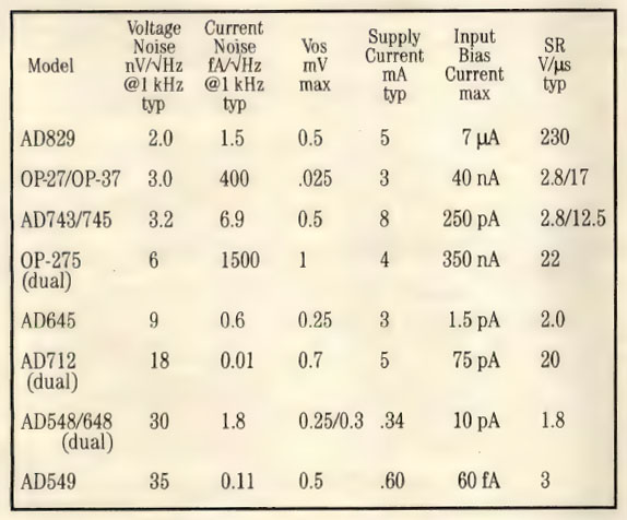
A 1992 Analog Devices advertisement compares the AD549's specifications to other low-noise op amps. The bias current of the AD549 stands out especially. It is by far the lowest of all types.


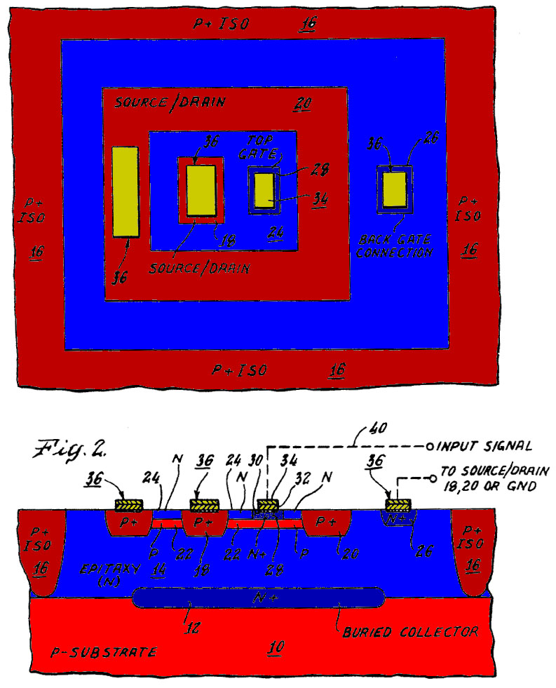
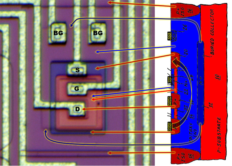
Analog Devices achieves the extremely low input current with the so-called "Topgate JFET Technology". The datasheet refers to the patent US5319227 "Low-leakage JFET having increased top gate doping concentration". This patent describes a special JFET and contains the above figure, which has been colored here for better understanding.

Much of the leakage current of an ordinary JFET occurs at the large interface between the gate and the substrate. In the top-gate JFET described in the patent, the upper part of the gate is isolated from the lower part. As will be shown, the input signal of the AD549 is connected only to the upper part of the gate. The small area and isolation from the substrate significantly reduces leakage current.


The package provides a guard pin that is only connected to the housing. If you do not want to increase the low input currents of the AD549 excessively by leakage currents, you have to surround the input potentials with shields which carry the same potential. This applies to the housing but also and especially to the circuit board. It is even better not to build the critical input pin with the input circuitry on the board at all, but to construct it on highly insulating spacers.

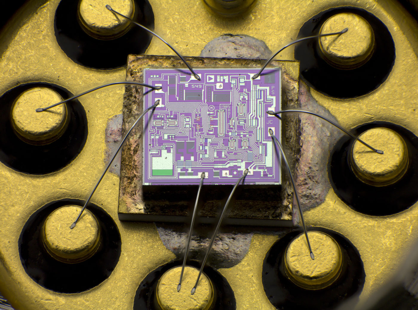
The negative supply potential is led to the die with two bondwires.


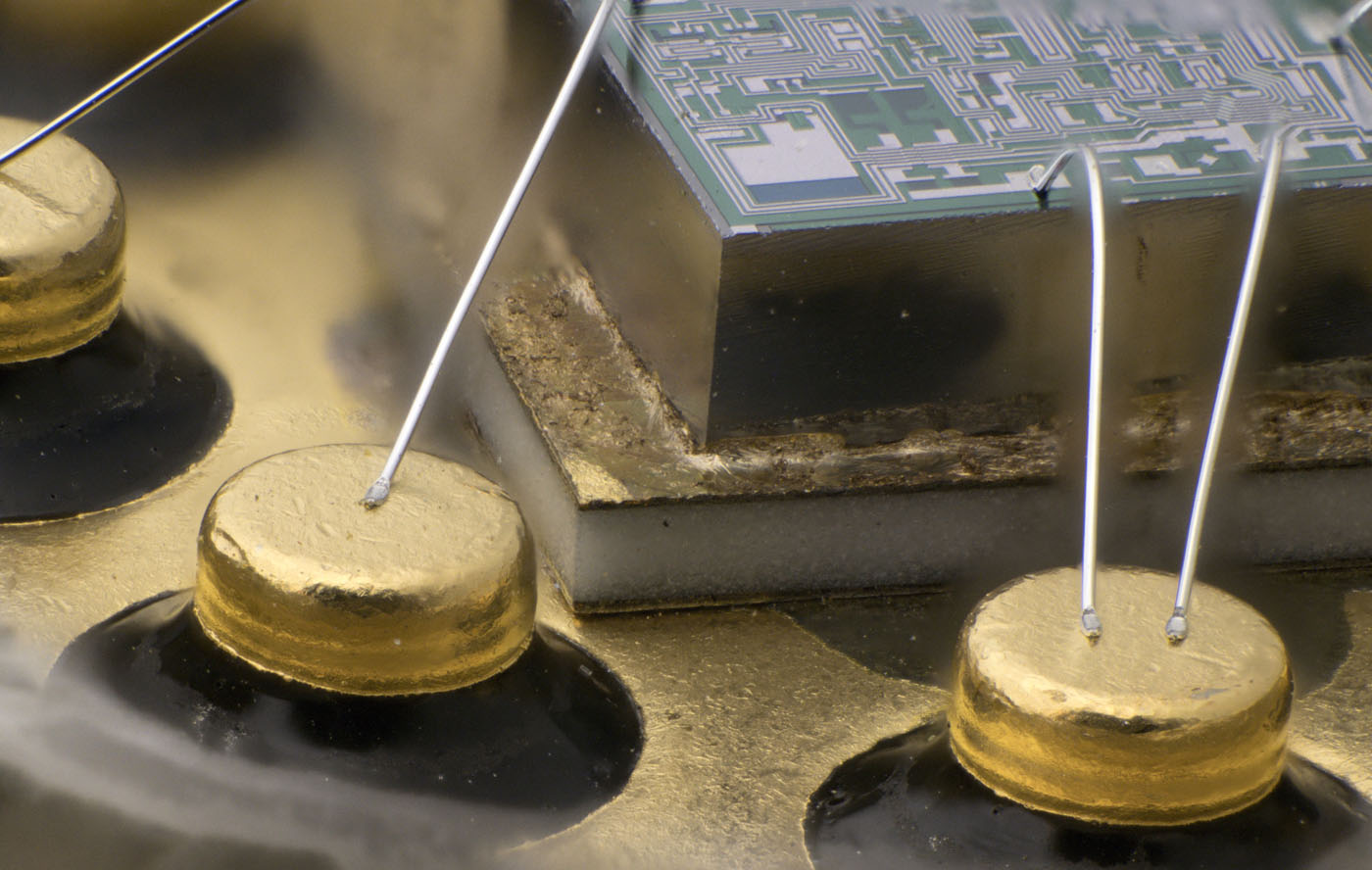
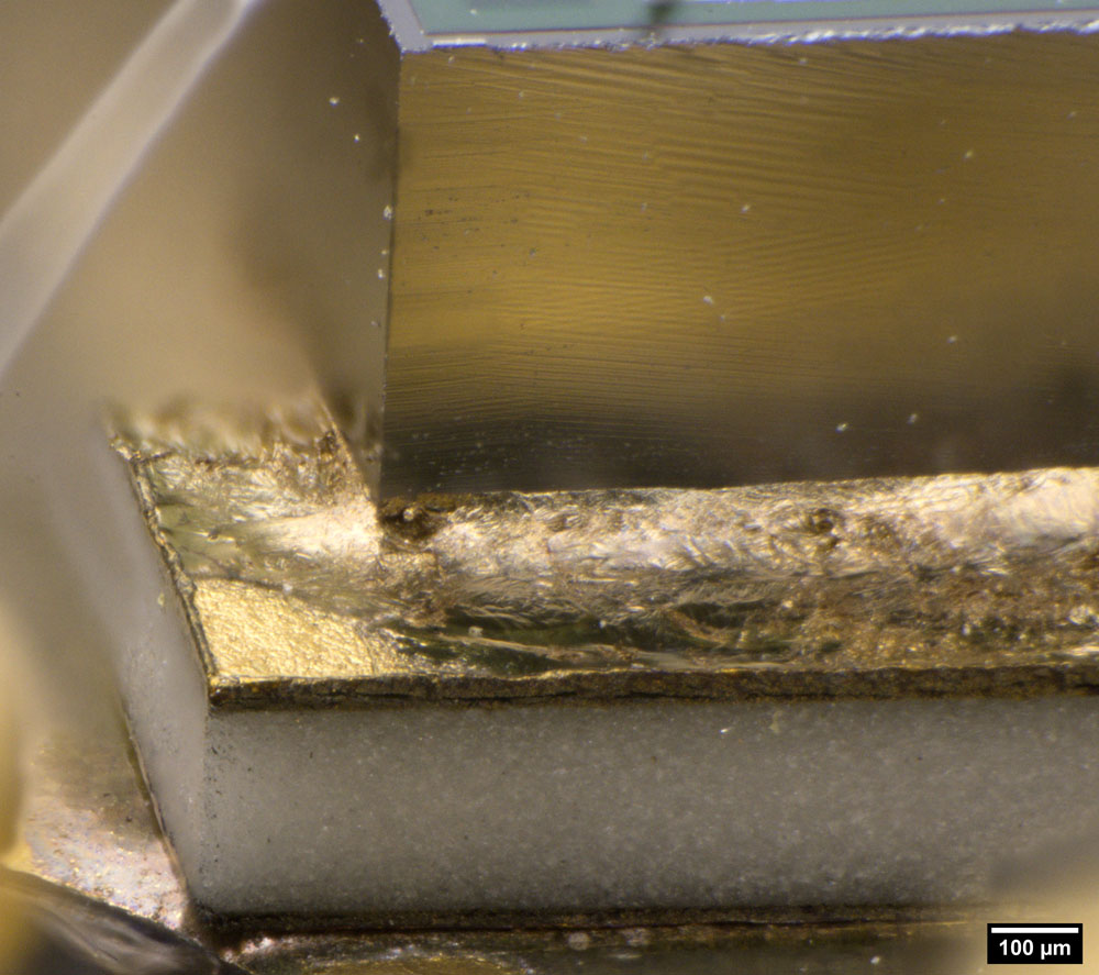
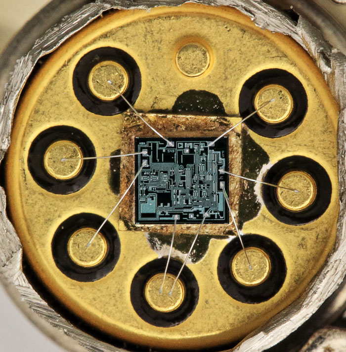
Since the guard potential is applied to the housing, the die must be isolated from the housing with a ceramic carrier.


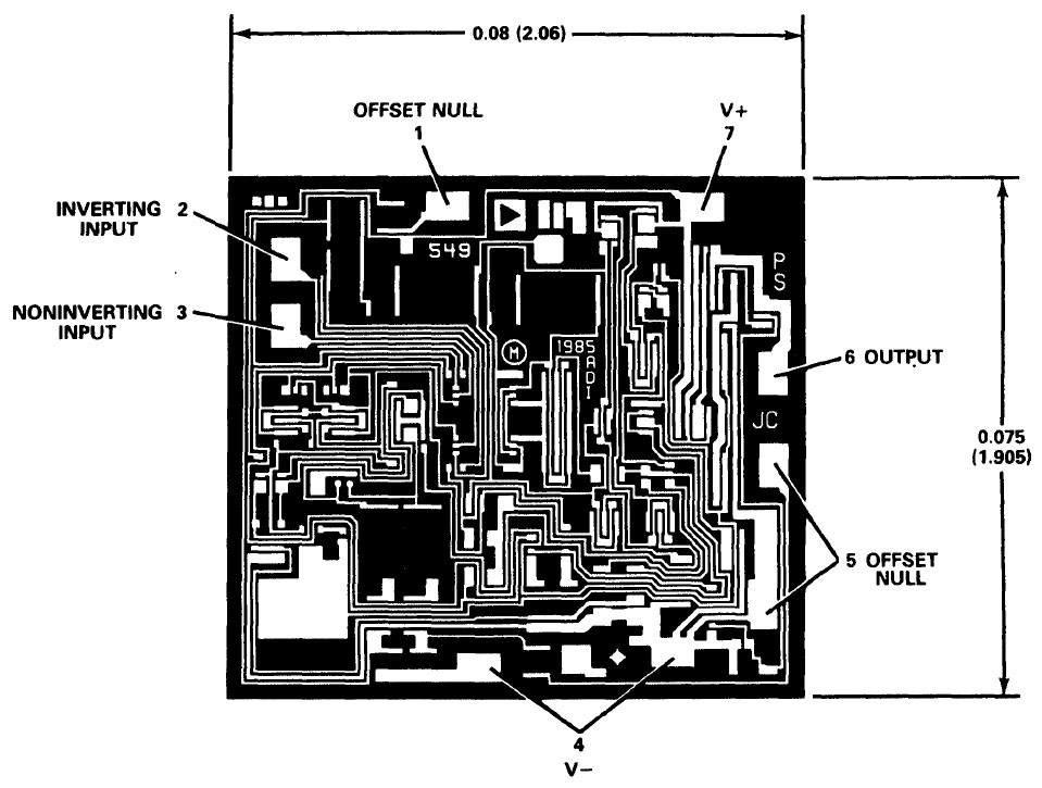
Older versions of the datasheet contain an image of the metal layer. The dimensions of the die are therefore 2,06mm x 1,905mm.


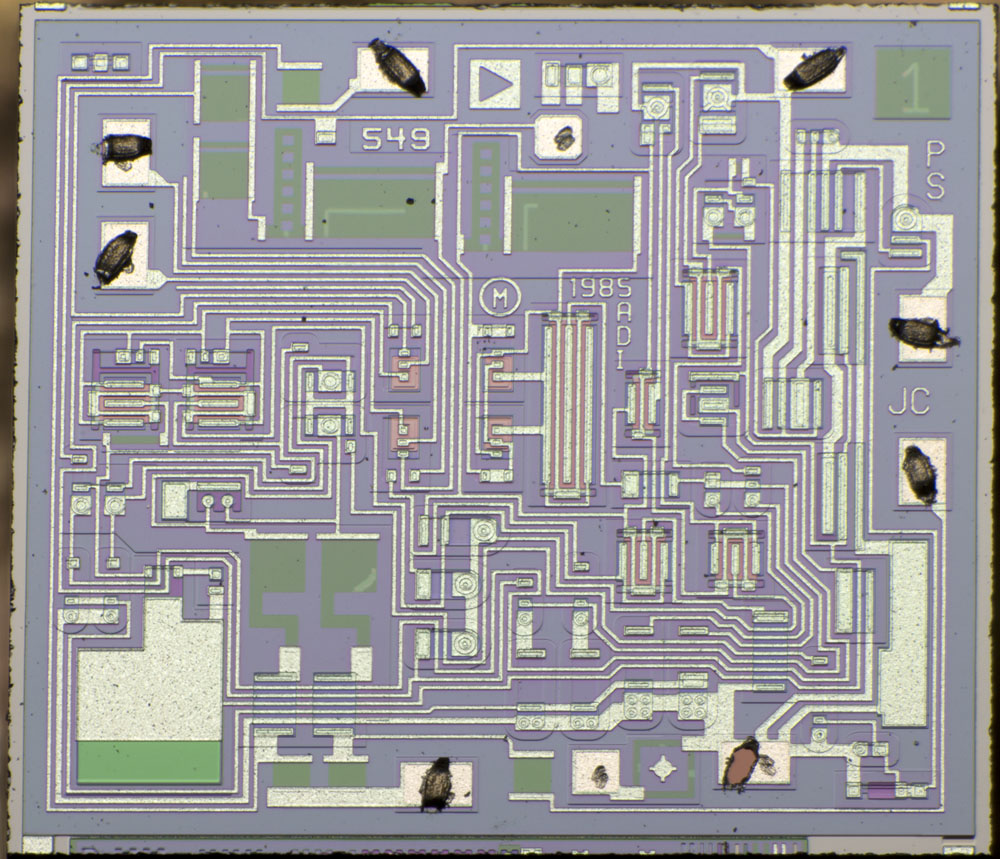
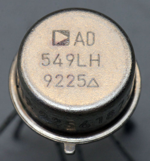
On the die there is the designation 549 and twice two letters that could be abbreviations of the developers. The design dates back to 1985.

Several resistors were calibrated with a laser. Typical for Analog Devices, there is a square with a testpad on the lower edge that is used to adjust the laser process and the number 1 is engraved in the upper right corner.


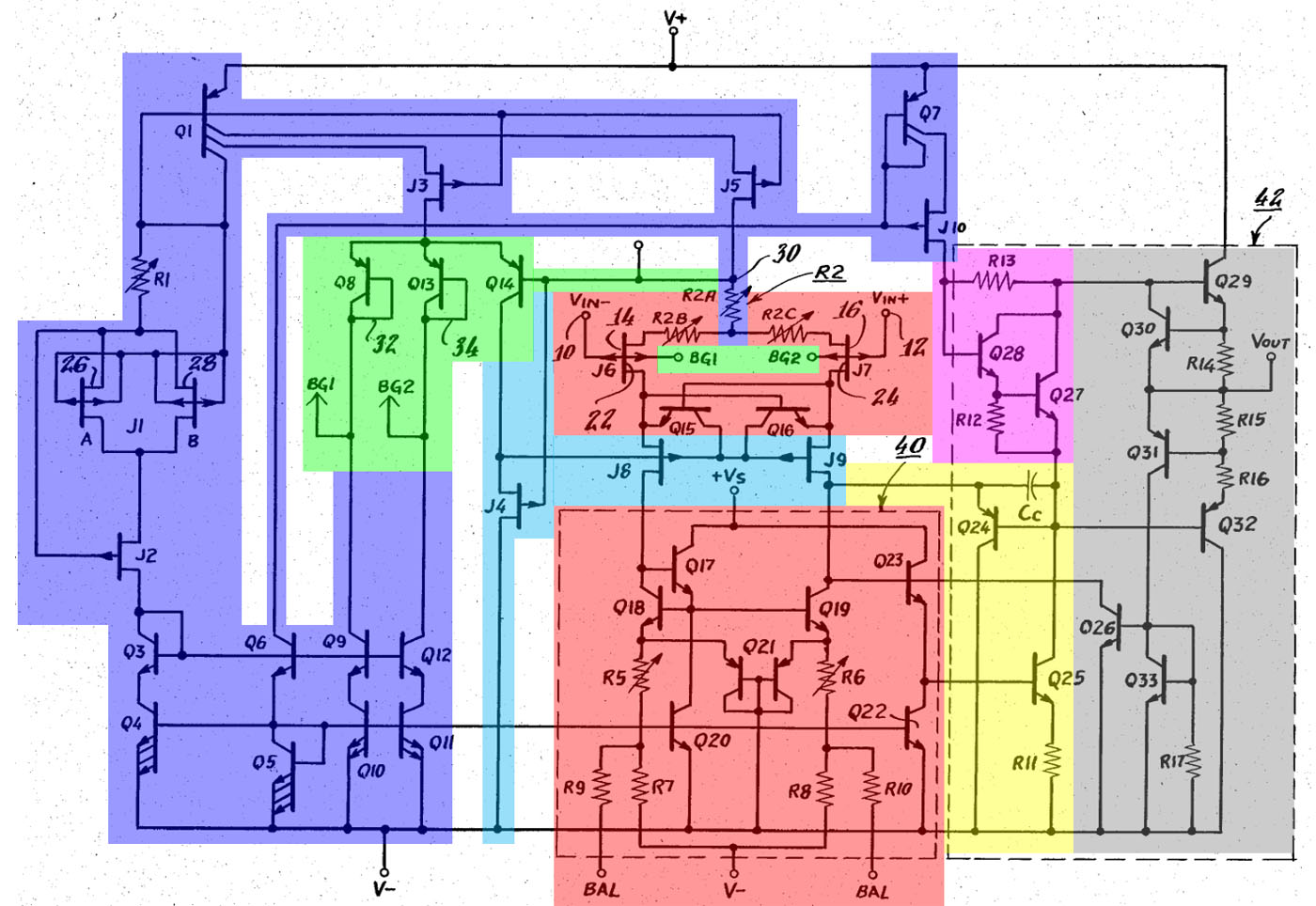
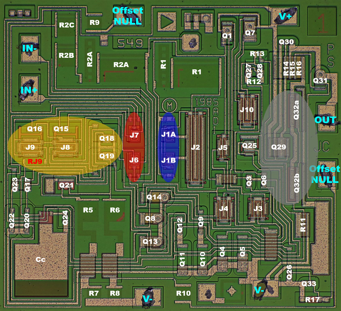
The datasheet of the AD549 does not contain a circuit diagram. However, it refers to the patent US4639683, which describes the above opamp. As will be shown, the schematic shown there matches the circuit in the AD549 except for one small detail. For better understanding, the individual function blocks have been colored.

The red block is the differential amplifier at the input of the OP549. The JFETs J6/J7 are the input transistors. They each have two gate terminals, of which just the top gate is connected to the respective input. The differential amplifier has its own V- potential. The double transistor Q21 guarantees that the potentials in this part of the circuit never rise too high. The transistors Q18/Q19 represent a current mirror with which the input transistors operate. Q17 generates the base current of the current mirror. Transistor Q23 forms the output of the differential amplifier with current sink Q22. Current sink Q20 appears to have been inserted in the left path to keep the circuit as symmetrical as possible.

Transistors Q15/Q16 probably reduce saturation effects when the input stage is overdriven. In this case, they open the cascode transistors J8/J9 (cyan), which otherwise shield the input transistors from the effects of common mode voltages.

The bias setting (blue) is relatively complex. It is based on the two JFETs J1A and J1B with resistor R1. The reference current generated across them is distributed to the circuit parts under J3 and J5 by transistor Q1. The cascode circuit with the JFETs isolates the current sources from voltage fluctuations. The reference current is further multiplied in the lower half by transistors Q3-Q6 and Q9-Q12.

Resistor R2A is balanced so that, in combination with the reference current, the same potential is present at testpad 30 as at the front gates of J6 and J7. Via transistors Q8/Q13/Q14 (green) this potential is transferred to the respective back gates. This ensures that front gate and back gate always have the same potential.

The input amplifier controls the voltage amplifier stage (yellow), which in turn controls the output stage (gray). The quiescent current setting (purple) reduces the crossover distortion. The power amplifier is supplied by its own current mirror consisting of Q7 and J10. Q30 and Q31 protect the output stage from too high currents. An overcurrent on the lowside does not directly reduce its output level, but the drive of the voltage amplifier stage.

An important point of the circuit is the adjustment. First, using resistor R1, the current through J1A/J1B is set to the value at which the temperature coefficient of the JFETs becomes minimum. Then R2A is adjusted so that the potential at point 30 is the same as at the front gates, i.e. the inputs of the AD549. This is necessary to get the same potential at the back-gates as at the front-gates. The JFETs J1A/J1B are constructed in the same way as the input transistors J6/J7. This ensures that production variations and drift effects affect both transistor pairs very similarly.

After the adjustment of the bias, the offset voltage and temperature drift of the input stage are adjusted. The resistors R5/R6 define the distribution of the currents to the two input transistors. Since the temperature drift of the JFETs depends on the drain current, the temperature drift of the offset voltage can be adjusted via this resistors. For this reason, it is not ideal for a JFET differential amplifier to adjust the offset voltage via the ratio of the drain currents, since this simultaneously changes the temperature drift of the offset voltage. Instead, the offset voltage of the AD549 is adjusted with the source resistors R2B/R2C. Because there is no easy way to vary the source resistors externally, the external offset adjustment is still done via the current distribution in the two branches. Accordingly, the datasheet indicates an additional temperature drift of up to 2,4µV/°C per adjusted millivolt of offset voltage.


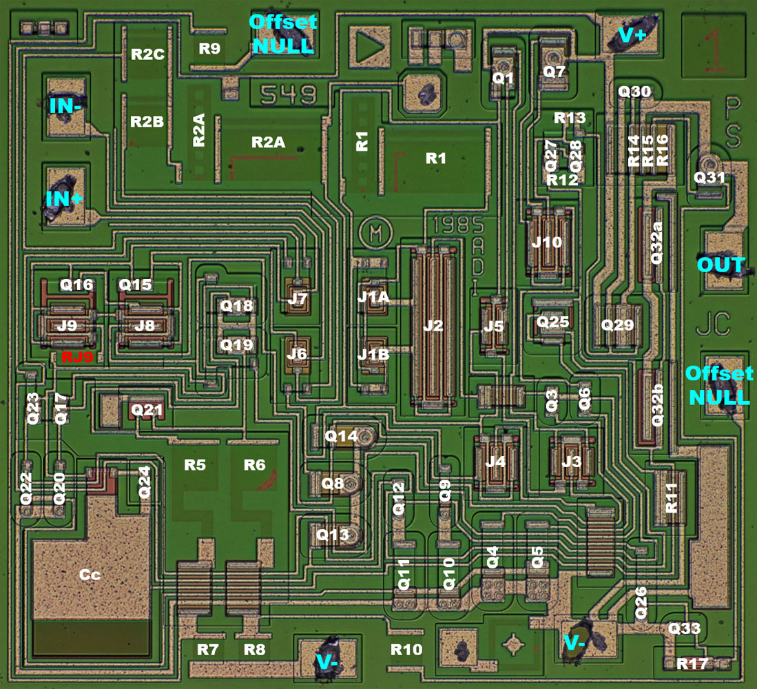
On the die all components from the schematic of the patent can be found. Just the resistor RJ9 is a small deviation. This resistor is located in the drain connection of the cascode JFET J9. It is from this branch of the differential amplifier that the signal is decoupled to the voltage amplifier stage. The resistor was obviously inserted quite deliberately. The purpose of the resistor remains unclear.


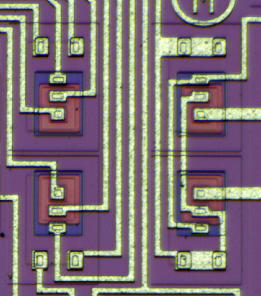
The JFETs in the input amplifier of the AD549 are located in the center (red). Directly next to them, the JFETs of the reference path are integrated (blue). The arrangement around the horizontal symmetry axis of the die reduces the effects of thermal gradients, which are generated to a large extent by the output stage (gray). There, the lowside transistor has been split into two transistors and arranged around the highside transistor. This measure guarantees that independent of the load of highside and lowside the power dissipation always occurs symmetrically around the horizontal symmetry axis of the die. The remaining critical transistors of the input amplifier are arranged on the symmetry axis too (yellow).


The two JFETs at the input of the differential amplifier and the two JFETs in the reference path are integrated so that they behave as equally as possible. A further improvement could only be achieved by splitting and cross-connecting the transistors, but this would increase the area of the input transistors too, which would then again have a negative effect on the leakage currents and parasitic capacitances.

Having the operating current of the JFETs set by identical JFETs is extremely advantageous. David Fullagar describes in the widely cited article "Better understanding of FET operation yields viable monolithic J-FET op amp" that production variations cause the drain current Idss of integrated JFETs to drift by a factor of 9. Accordingly, it is difficult to define an ideal operating current in a design.


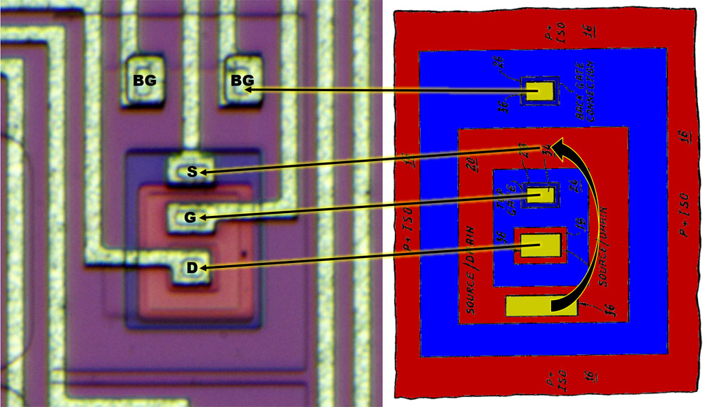
If you compare the structures with the patent US5319227, the parallels are easy to see. Just the source contact is not on the outside in the AD549, but between the top-gate and the back-gate connection.


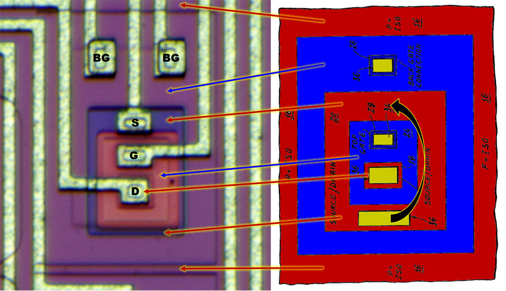
The structures cannot be immediately assigned at first glance. This is mainly due to the fact that the colors on the die are partly inverse to the usual colors for n- and p-doping.

The outermost square frame is the boundary between the n-doped well and the heavily p-doped insulating layer surrounding the transistor. The n-doped well carries the potential of the back gate.

The dark blue frame contains the strong p-doping, which is the larger, outer source electrode. Below the center drain contact is the same doping, but it is hidden by the metal layer.

The red area is the n-doped top gate. Below it is the channel between source and drain. At the transitions from the red gate area to source and drain, a kind of frame can be seen. Probably there the gate area overlaps the highly doped contacts to the actual channel. So you can be sure that the channel is completely covered by the gate.

The buried layer with its strong n-doping, which is used as a collector feed line in NPN transistors, is just visible as a step in the surface.


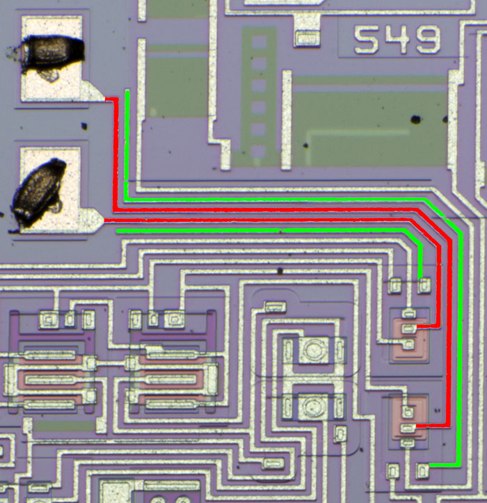
The two lines from the inputs of the AD549 to the JFETs of the differential amplifier (red) are shielded with the potentials of the back-gates (green). This reduces the parasitic capacitances and probably also the leakage currents to some extent.


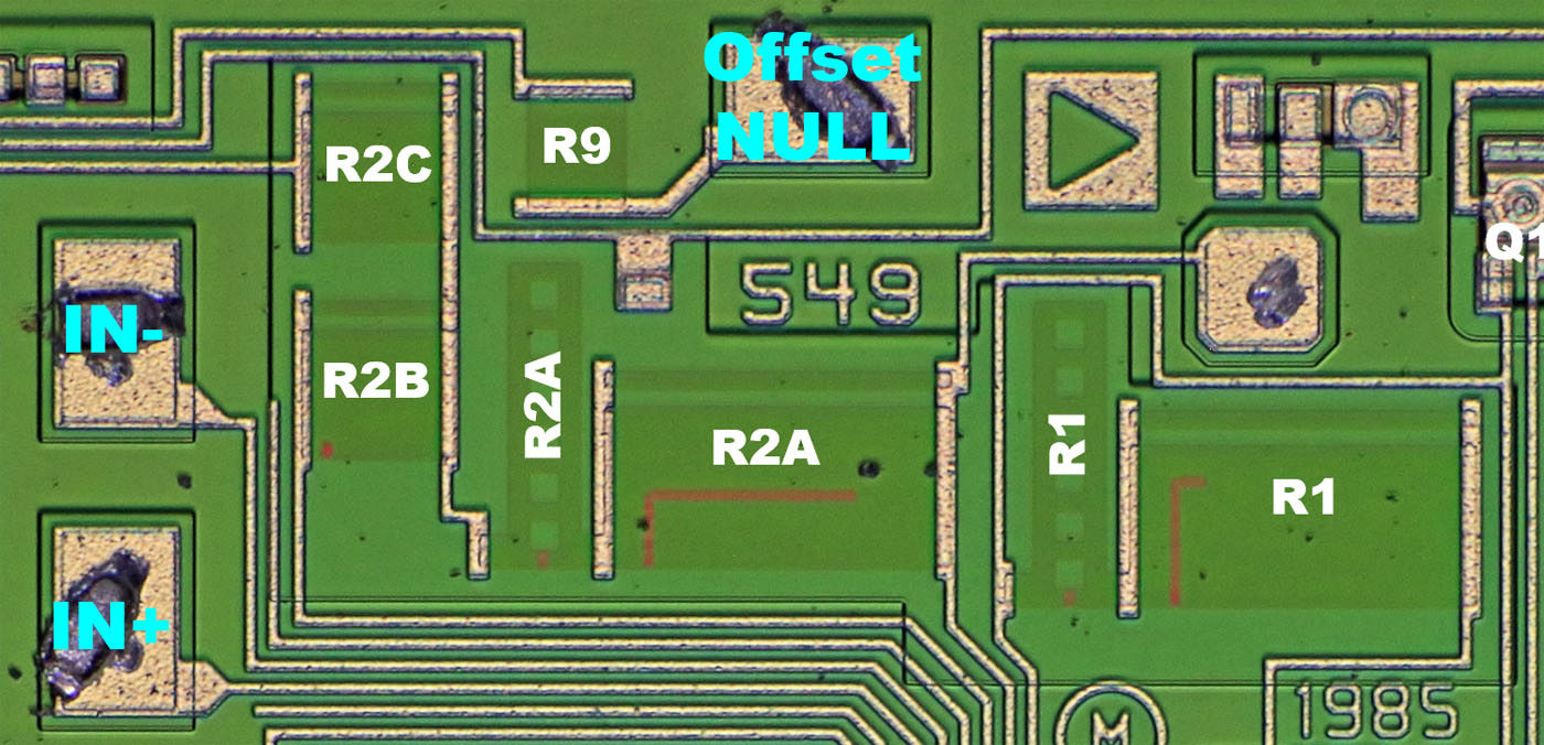
Resistors R1 and R2A each consist of two elements that allow more extensive adjustment. A test point allows to measure the potential above resistor R2, which is necessary to adjust the synchronization of reference current source and input stage.


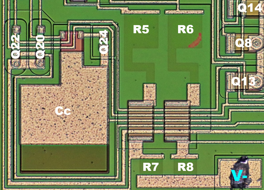
The resistors R5/R6, which are used to adjust the offset drift, provide a less complex structure. The traces of the adjustment are clearly visible.

The design offers the possibility to increase the capacitor Cc and thus adjust the frequency response.


The bipolar transistors Q15 and Q18 are directly integrated into the structures of the JFETs J9 and J8.


https://www.richis-lab.de/Opamp61.htm

 :-/O
 
The following users thanked this post: SeanB, TiN, ANTALIFE, Gyro, snik, RoGeorge, iMo, sansan

Offline Gyro

  • Super Contributor
  • ***
  • Posts: 9501
  • Country: gb
Re: Opamps - Die pictures
« Reply #349 on: December 23, 2022, 08:19:08 pm »
While you're on very low input current opamps, it would be interesting to see the LMC662, it has a typical 25'C input current of 3fA and is cheap. There has been some discussion here as to whether its input protection networks are bootstrapped or not.

You tend to find them scattered liberally in the high impedance sections of commercial picoammeter and SMU type products, eg. https://www.eevblog.com/forum/metrology/project-for-standalone-use-of-keithley-low-current-preamplifier/
Best Regards, Chris


Share me

Digg  Facebook  SlashDot  Delicious  Technorati  Twitter  Google  Yahoo
Smf