The labelling of this component has been ground off. As will become apparent, it is the dual opamp TLC2262 from Texas Instruments. The datasheet specifies a supply voltage range of +/-2,2V to +/-8V, whereby single supply is also possible. The current consumption is typically 400µA. The TLC2262 offers a rail-to-rail output. Absolute Maximum Ratings specify 50mA as the output current. Typically, the currents are much lower. If one approaches the supply potentials, the maximum possible current also drops sharply.
The relatively low noise of 40nV/√Hz (10Hz) or 12nV/√Hz (1kHz) is emphasised. The offset voltage is typically 300µV with a temperature drift of 2µV/°C. At room temperature, a bias current of 0,5pA can be expected. The low current consumption of the opamp is noticeable in the speed. The bandwidth is only 0,71MHz. The maximum possible slewrate is typically 0,55V/µs.
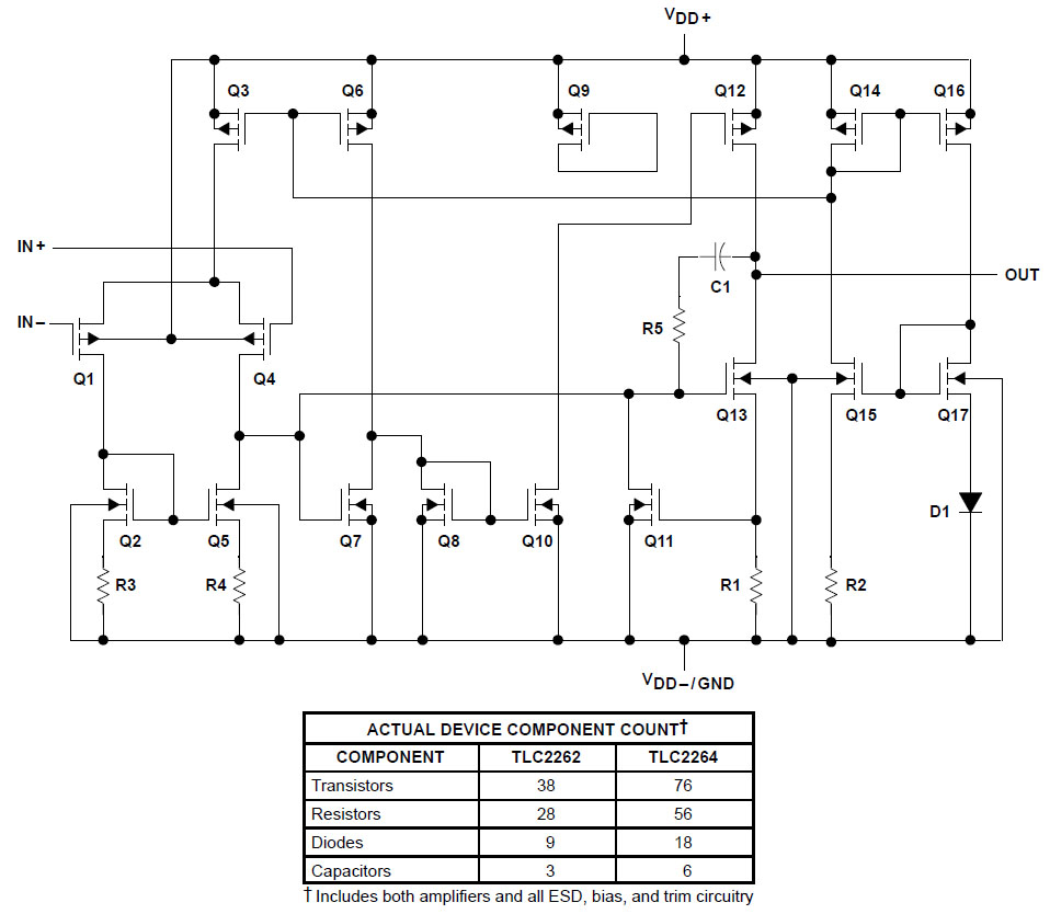
The datasheet contains a circuit diagram that shows a very clear circuit. The circuit section Q14-Q17 on the far right generates a reference voltage that ensures that Q3 and Q6 behave like current sources. The differential amplifier Q1/Q4 at the input works against the current mirror Q2/Q5.
The output of the differential amplifier directly controls the lowside transistor Q13 at the output. R5/C1 limits the frequency response and thus stabilises the circuit. Q11 represents a current limitation with R1.
The connection of the highsidetransistor Q12 and the transistors Q7-Q10 seems illogical, but it becomes clearer in the following if you look at the circuits of the related opamps.
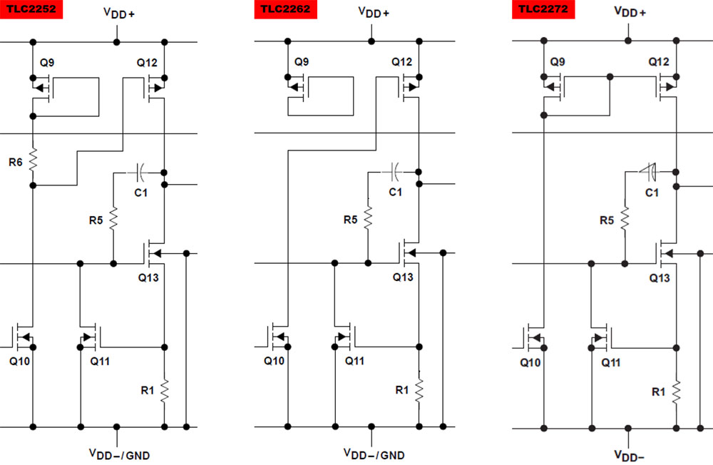
In addition to the TLC2262, Texas Instruments also offers the TLC2252 and the TLC2272. The TLC2252 typically consumes only 70µA, but also offers a slewrate of just 0,12V/µs and a bandwidth of 0,2MHz. The TLC2272, on the other hand, draws 2,2mA and thus enables a slewrate of 3,6V/µs and a bandwidth of 2,18MHz. The TLC2262 represents the compromise of both types: 400µA / 0,55V/µs / 0,82MHz. With increasing current consumption, the noise of the opamp is also reduced.
The datasheets of all three opamps contain circuit diagrams that only differ in the wiring of the transistors Q9 and Q12. In the TLC2272, transistors Q12/Q13 form a push-pull output stage. Q12 is controlled from the differential amplifier at the input, whose signal is transmitted to the output stage via transistors Q7-Q10. Q9 and Q12 form a current mirror here.
In the TLC2262, transistor Q9 is isolated from the rest of the circuit. Since the control of Q12 lacks any pull-up structure, Q12 behaves like a current source in the TLC2262. Consequently, the output stage operates in class A mode. The maximum possible current change at the output is reduced accordingly, but the current consumption of transistor Q9 is saved.
In the TLC2252, Q9 is integrated into the circuit again. The resistor R6 has been added. This results in the same function as in the TLC2272, but with a reduced current. The combination of the more efficient class B operation of the output stage with the reduced current through Q9 obviously results in a minimal current consumption. Now, however, the highsidetransistor must be charged with the low current of Q9, which significantly reduces the speed of the opamp.
The advantage of these modifications is that one just has to make small changes to the circuit to be able to represent three different opamps.
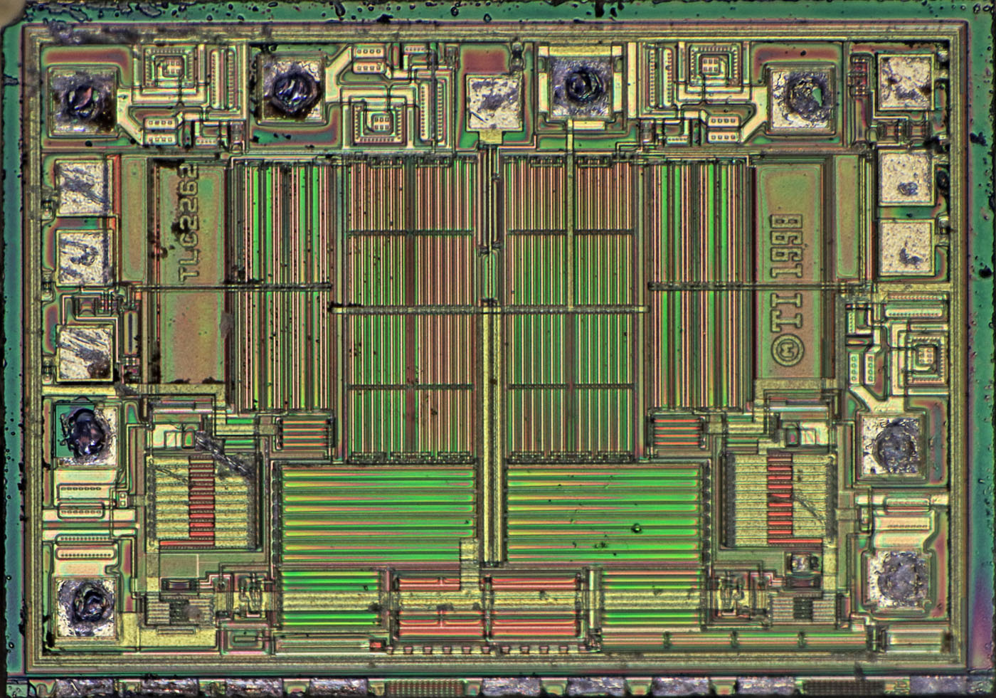
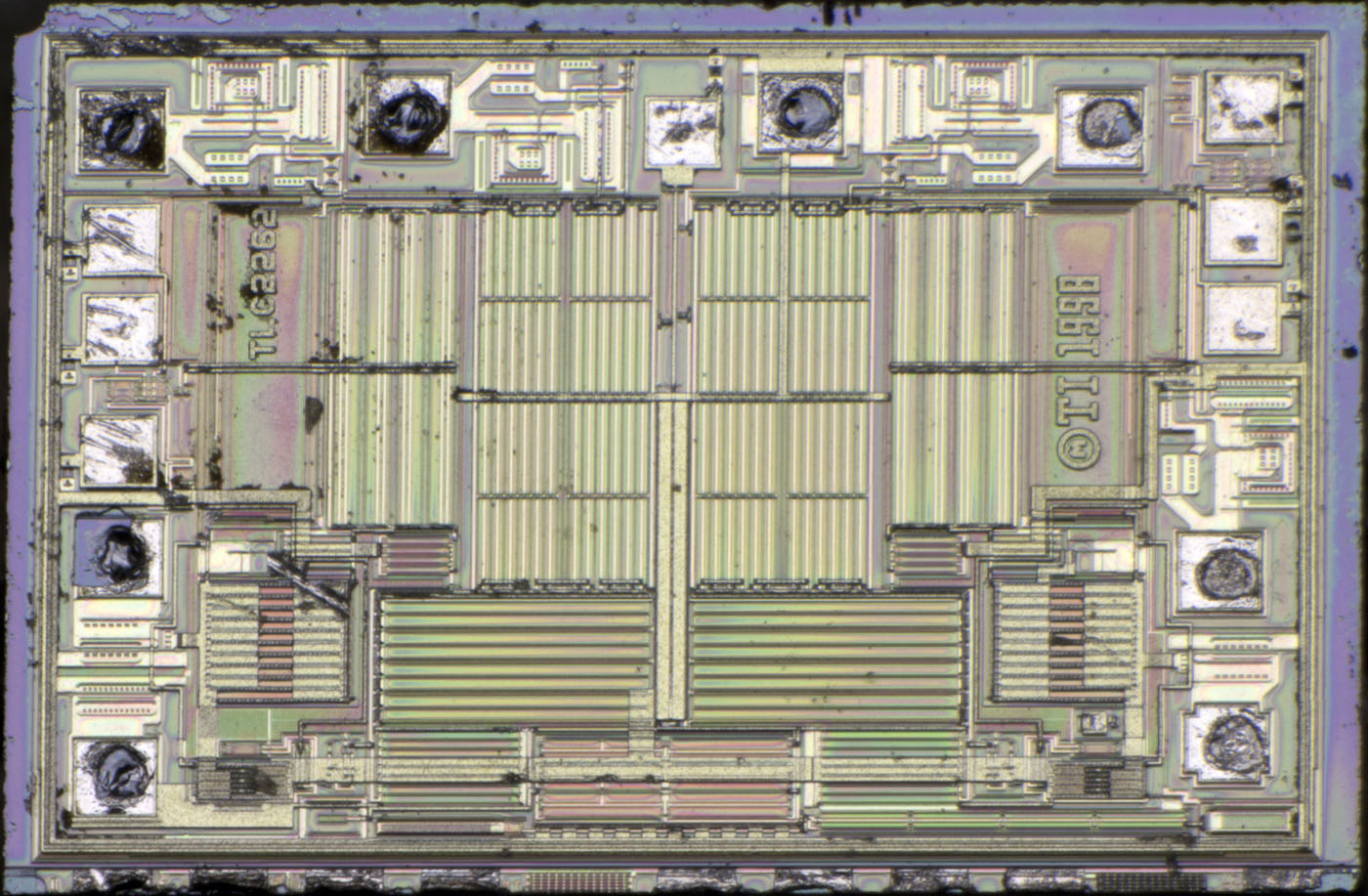
The dimensions of the die are 2,3mm x 1,6mm. It is manufactured using the so-called "Advanced LinCMOS" process. A more detailed analysis of the circuit is difficult due to the small structure sizes and the two metal layers.
The dichotomy of the die is clearly visible. The inputs with their extensive protective structures can also be clearly identified. The large structures in the middle of the die appear to be the transistors of the input stage. On the right and left edges there are three testpads each, which are clearly used to adjust resistors. Above them, the offset voltage is most likely adjusted via resistors R3/R4.
The function of the central testpad on the upper edge remains open. Since it apparently influences both opamps, it could be that the bias is adjusted over it.
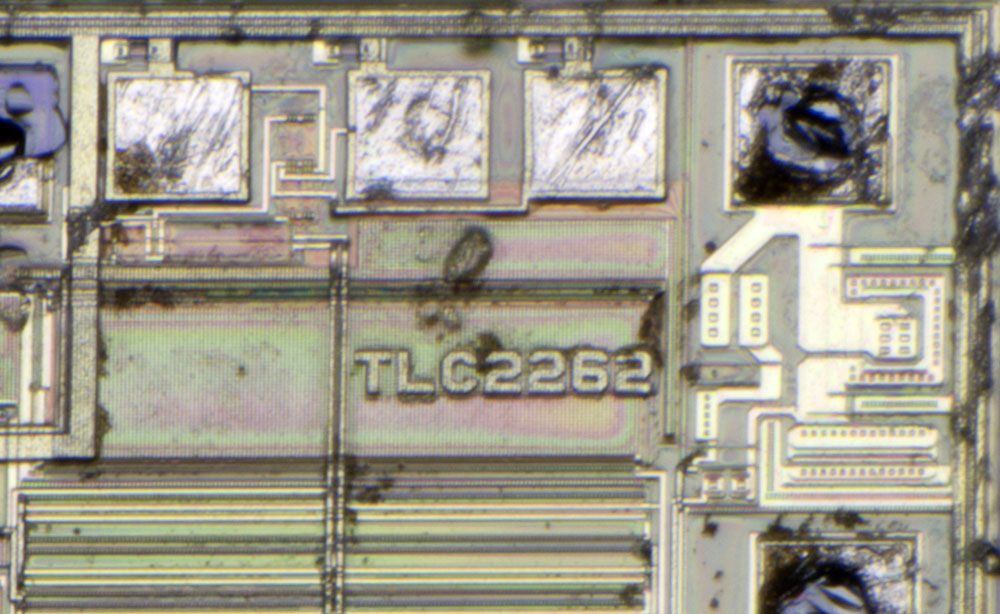
The die is marked with TLC2262. In principle, one cannot be sure in such a case whether it is not just a basic variant that can also be configured as TLC2252 or TLC2272. Most likely, however, it is a TLC2262 and the variants TLC2252 and TLC2272 are represented by variations of the metal layer, which then can be given their own designations. It hardly seems conceivable that the one testpad is sufficient to switch between the three different circuit variants.
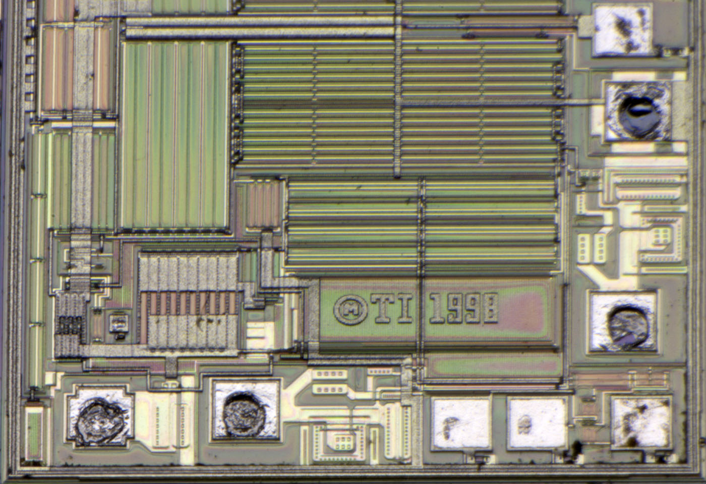
The design dates from 1998. In the lower left corner at the output bondpad, the output stage can be seen. The highside transistor is surprisingly small.
https://www.richis-lab.de/Opamp69.htm 


