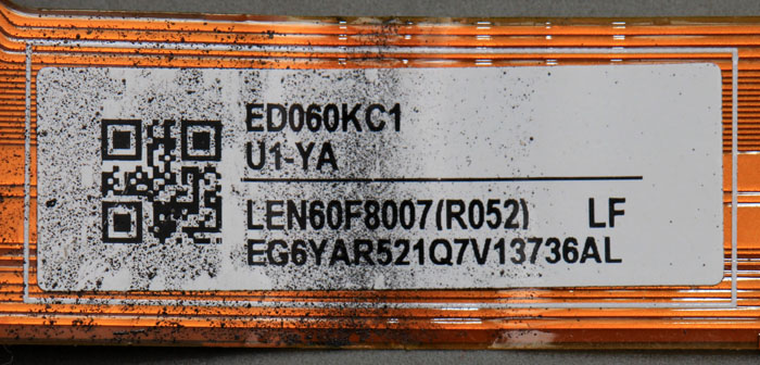
The ED060KC1 is a e-paper display used in the Kindle Paperwhite 3. It supplies you with a 16 greyscale 1072 x 1448 resolution.
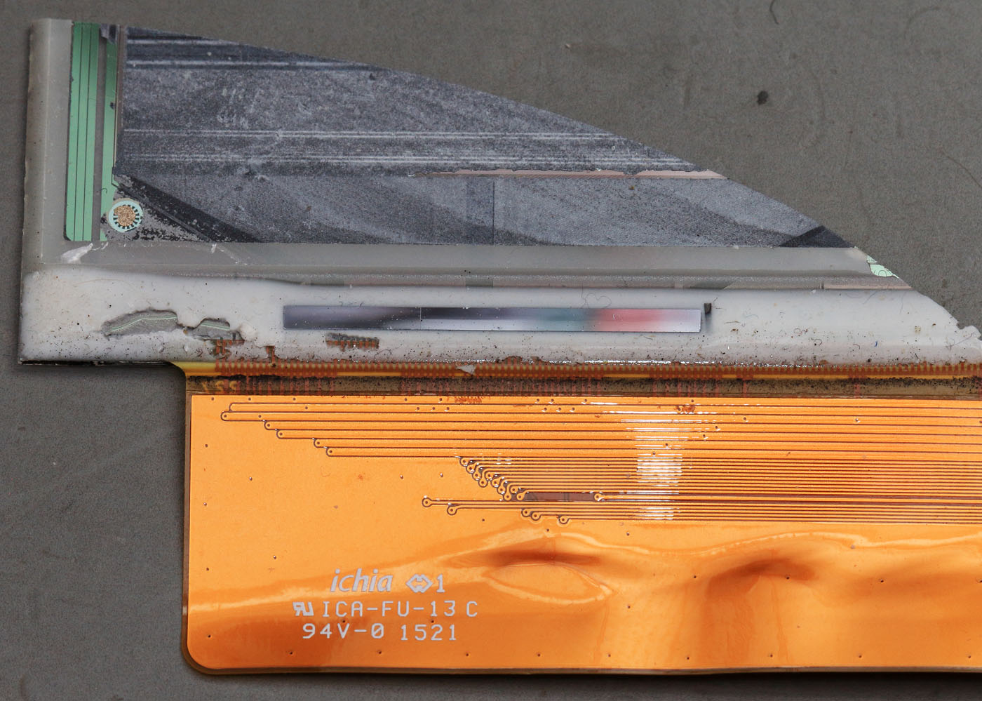
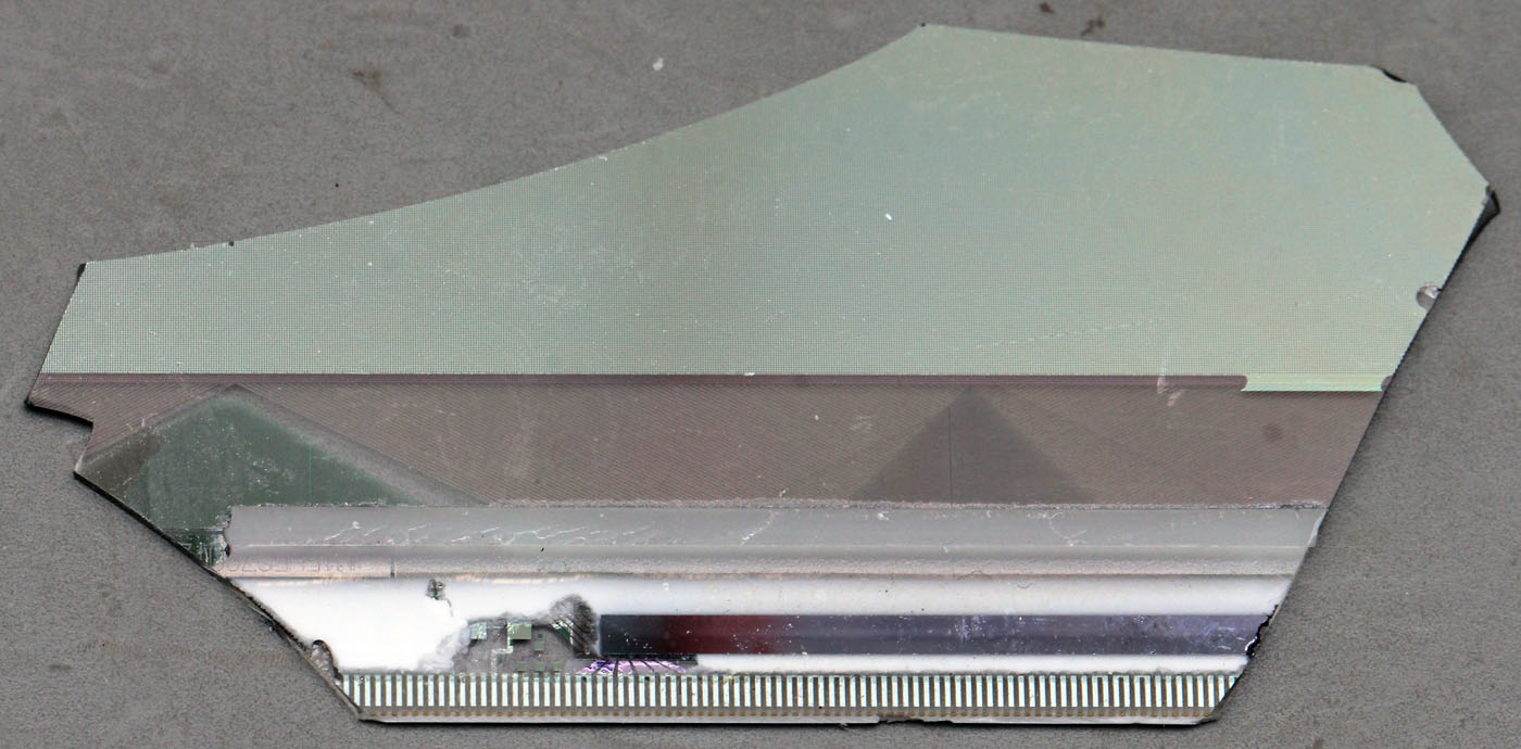
I own a fragment of the display. The top glass is already removed. We see the lower glass with the TFT electronics and the active mass.
If we turn the glass we see the undermost metalisation of the upper side.
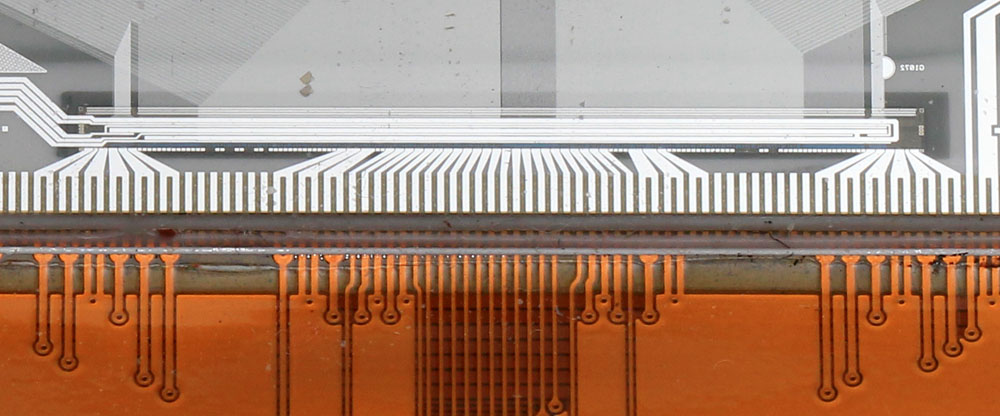
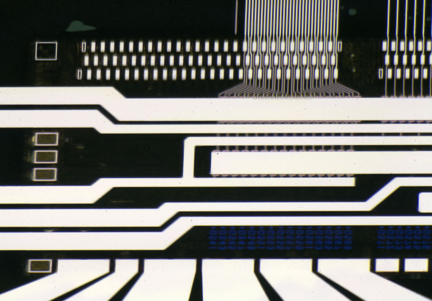
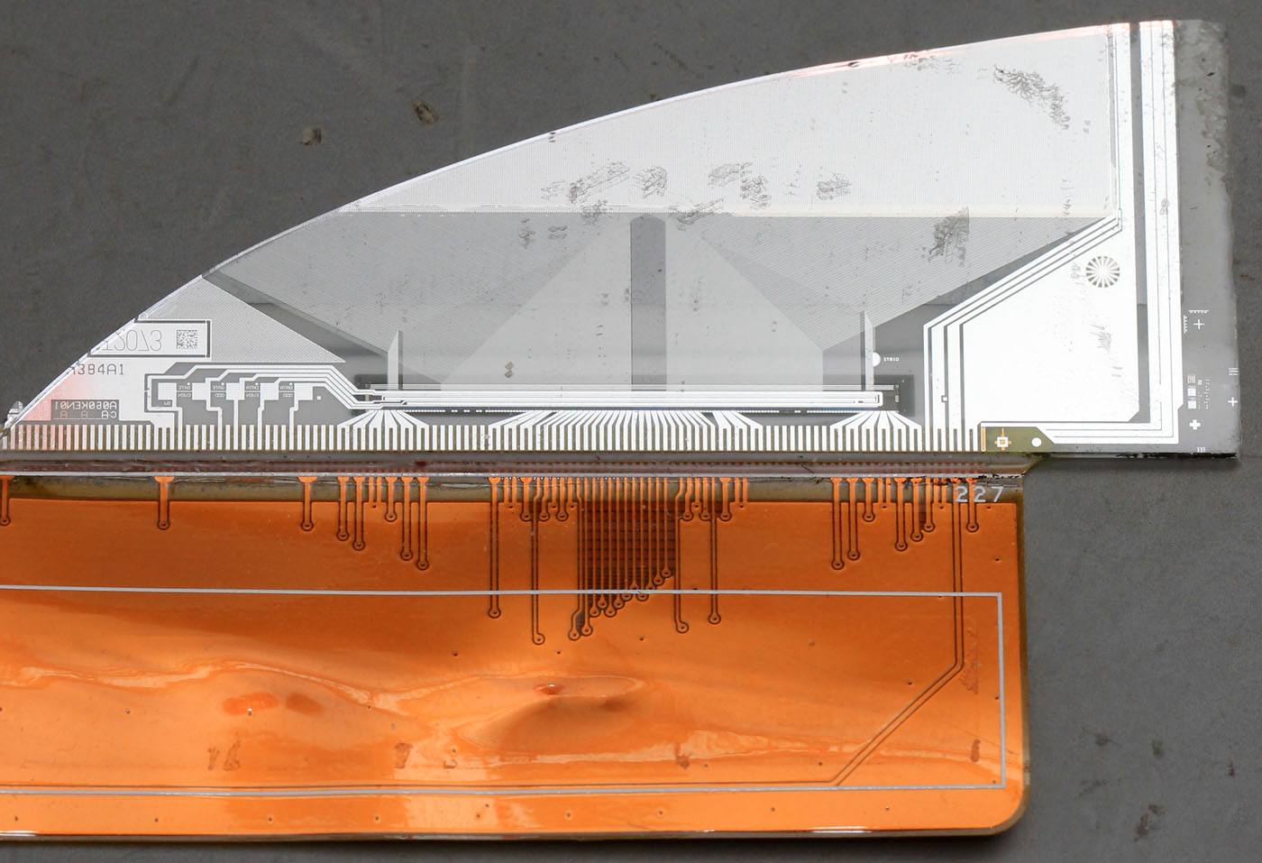
Here is the controller. Some tracks come from the flex connector and a huge amount of signals travel to the display.
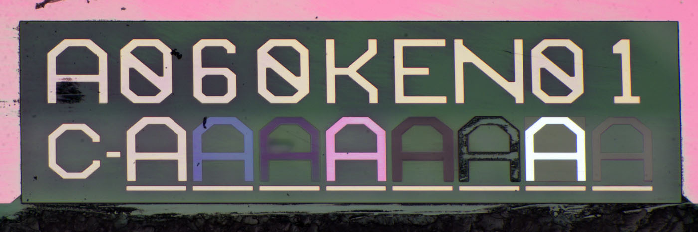
Probably A060KEN01 is the panel name.
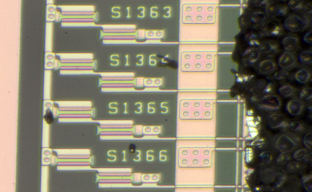
We see eight mask revisions.
Is everything aligned properly?
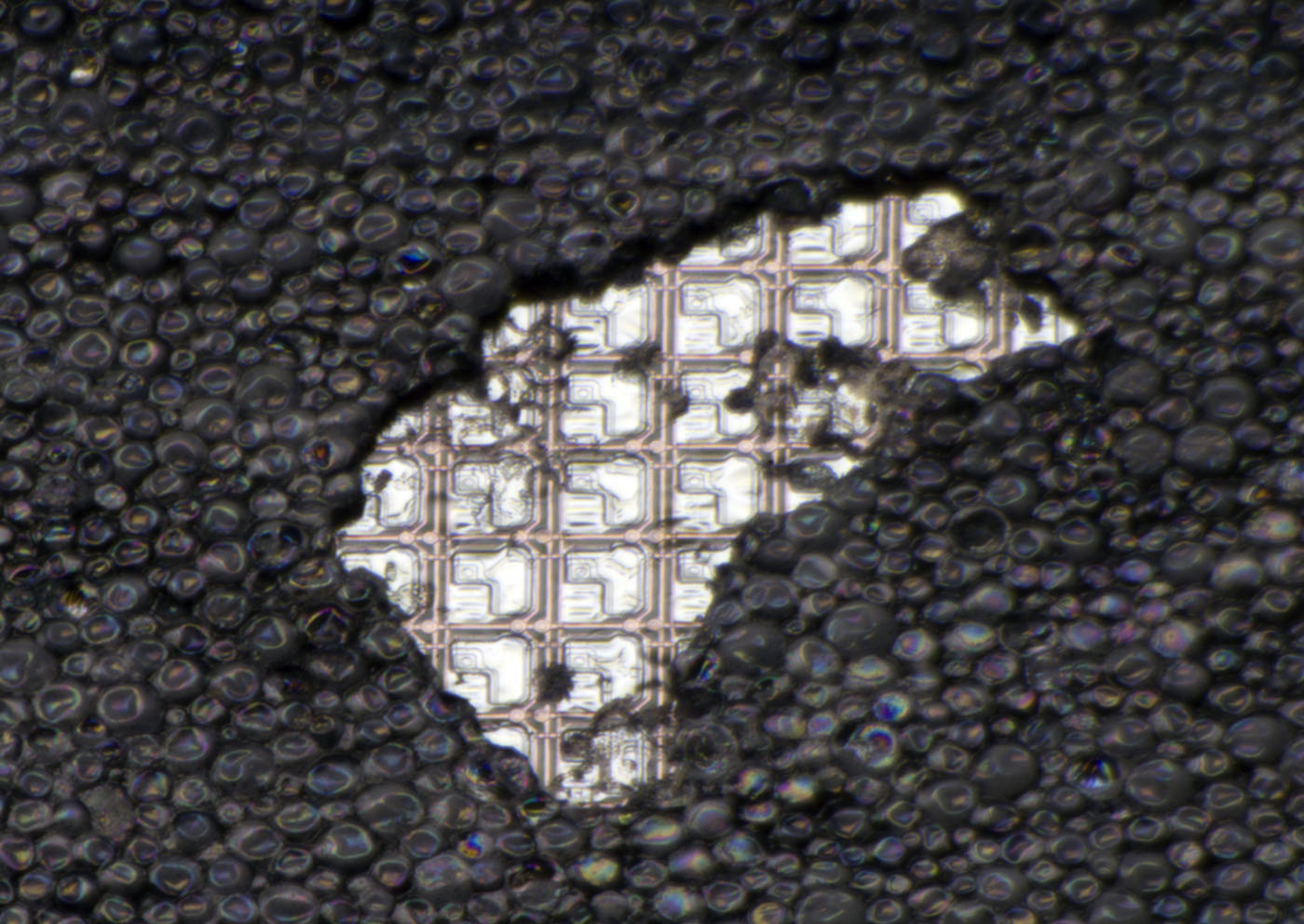
Probably that´s the contact connecting the upper glass that is just the upper electrode for the whole display.
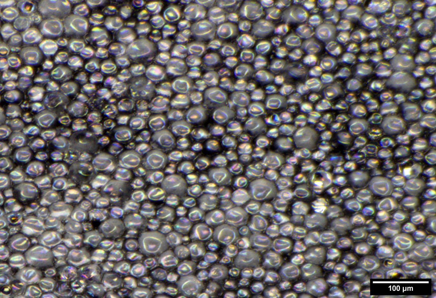
The active mass consists of bubbles with a diameter of up to 60µm containing pigments that travel through the bubble depending on the electrical field. Then the bubble is dark or bright.
Under the thin layer of this active mass we have the TFT circuit.
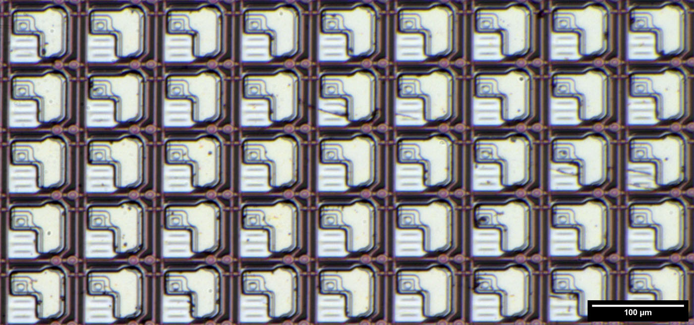
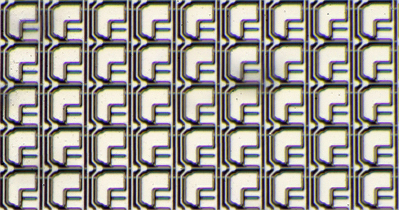
Datasheet says the dot pitch is 84µm.
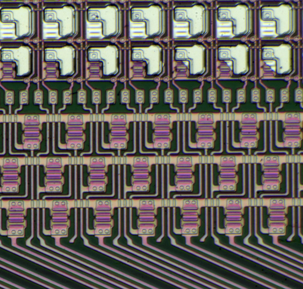
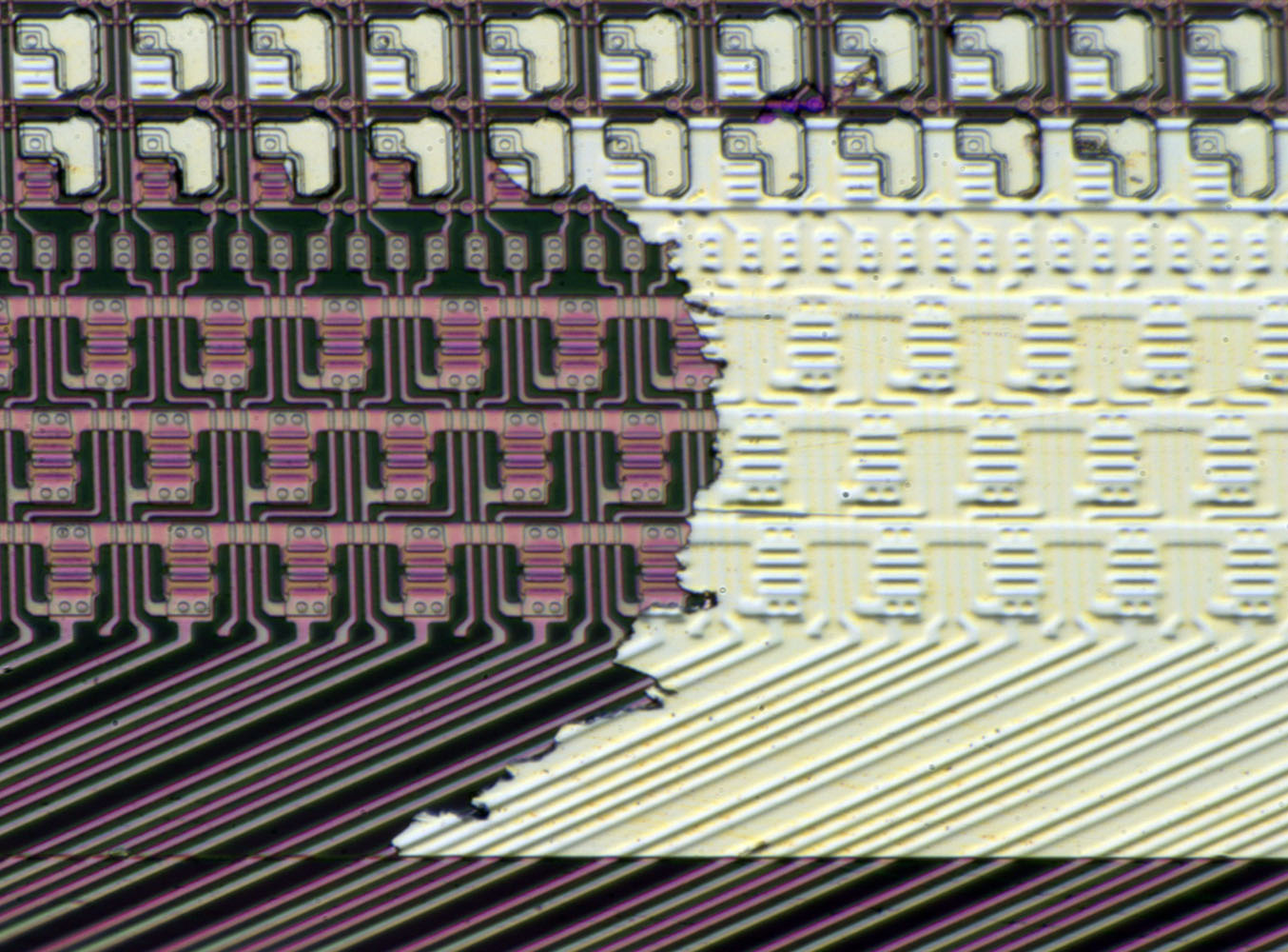
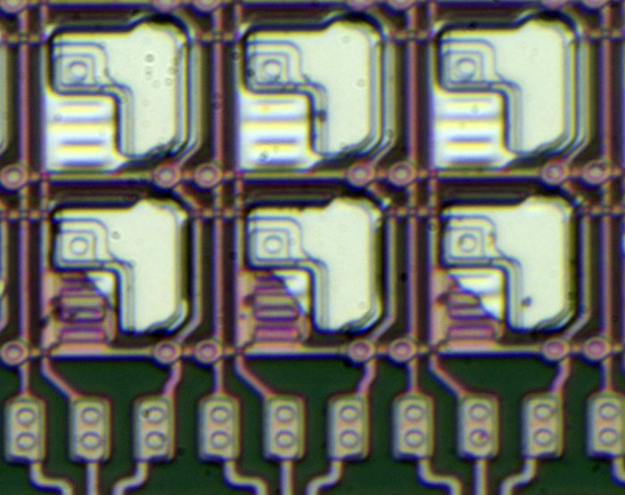
The bright area is the upper electrode controlling the electrical field around the active mass.
On the upper electrode we see the contours of a capacitor (the bigger area) and the pixel switch (the smaller square).
You need a capacitor because the pigments in the bubbles are quite slow but you want to switch the pixel fast.
Around the pixel there are supply and control lines. There are two horizontal lines. One line is the reference for the capacitor in the pixel, one is the activation line for the whole row.
There are three vertical lines. One line is controlling the gates of the transistors of the pixel column. The other two lines seem to be connected to every horizontal line. That can´t be true because then it would be impossible to address one single line. It seems like the controller is selecting the pixel rows by these additional vertical lines. In pictures of the complete display you can´t spot a controller on the sides of the panel.
From the bottom of the glass we can take a look at the undermost metal layer. We clearly see the two gate electrodes of every pixel. You need two electrodes because TFT transistors have a high leakage current. With the high voltage (something around +/-10-20V) the current flow would degrade the pixel status.
On the left side of the panel the capacitor reference is connected directly to one big metal line. The row selection line is connected to two transistors probably acting as a pull-up or pull-down.
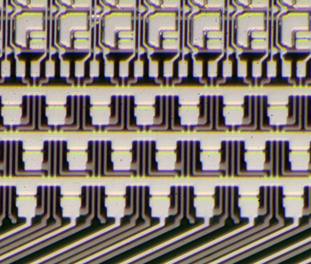
On the lower part of the panel there are three big lines acting as pull-up or pull-down for the control lines.
Not every line is connected. That is plausible because for 1072 x 1448 dots you need 1,35 row control lines for every column control line.
There seems to be a lack of metal on the lowest pixel row. In one place there is a huge amount of metal. Probably the lowest line is a dummy line like we have seen that in the DLP-Modul DMD1076 (
https://www.richis-lab.de/DLP.htm) and in the Lepton 2.5 (
https://www.richis-lab.de/Opto04.htm).
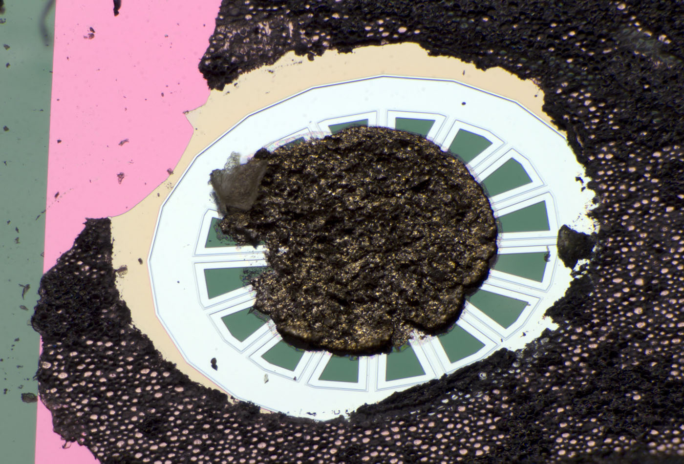
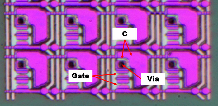
Fortunately here we can see the two transistors.
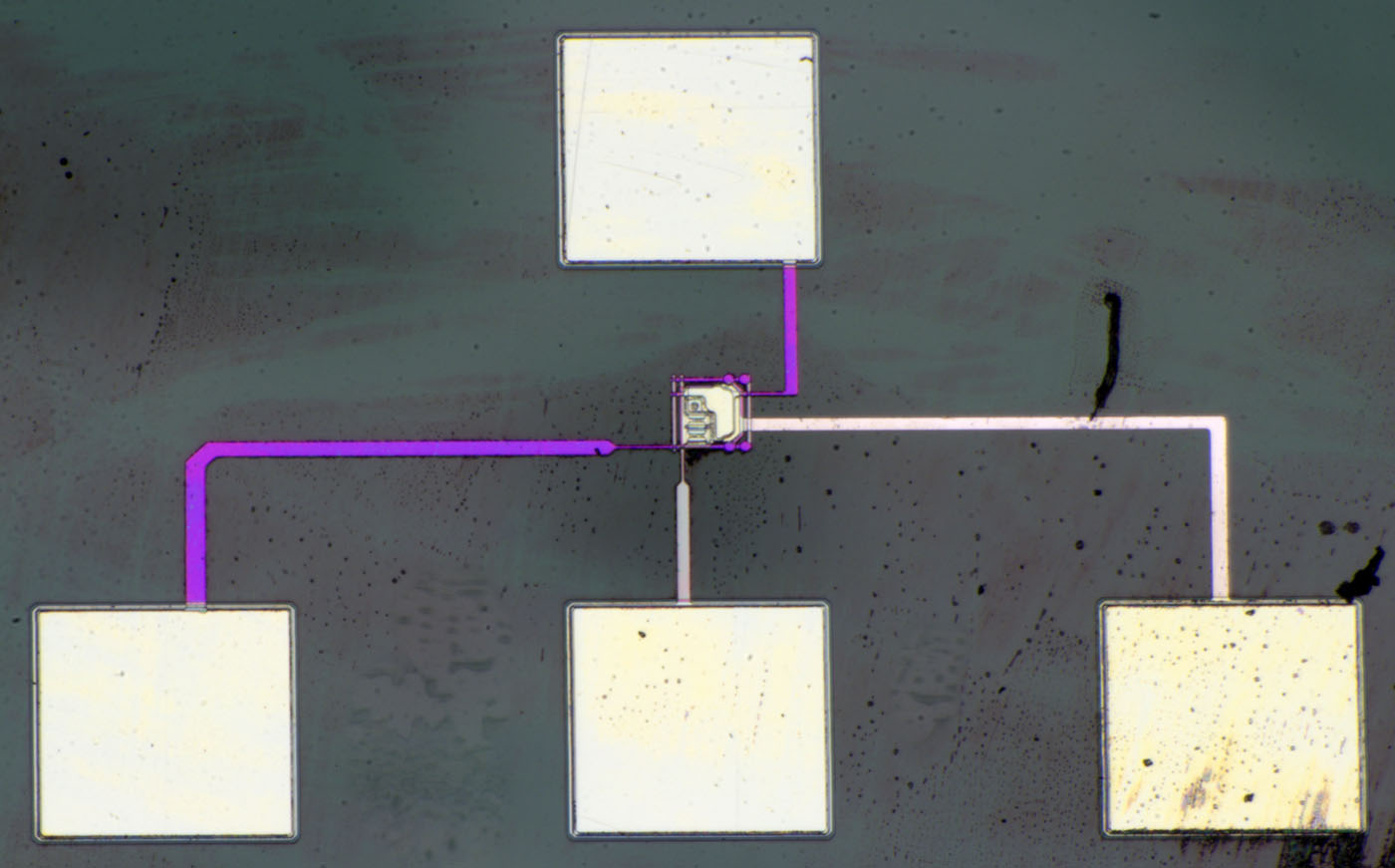
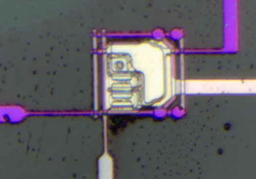
A test structure! With the bottom pad you can switch the pixel. The left pad supplies the pixel. The upper pad is the reference for the capacitor and the right pad is connected to the upper electrode.
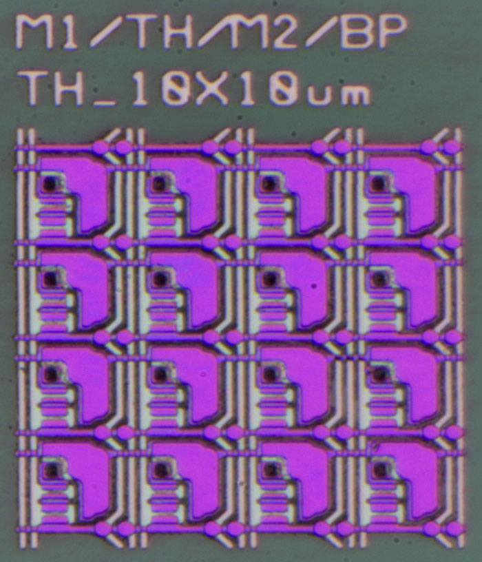
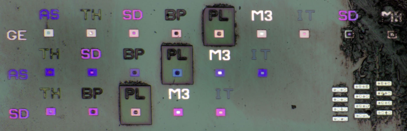
On the edge of the panel we have some nice test structures showing the construction of the panel.
Here we see M1 and M2 showing us the metal parts of the MOSFETs.
TH probably stands for through hole and gives you 10µm vias. It seems that is a little too much.
I don´t know what BP means.
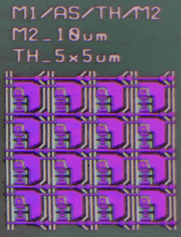
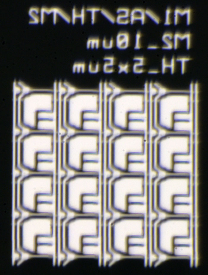
Here we have AS. That probably stands for amorphous silicon that is located in the MOSFET area.
Vias are smaller here. Looks good now.
It seems M2_10µm stands for a different transistor type. The contacts between the MOSFETs are smaller in this area.
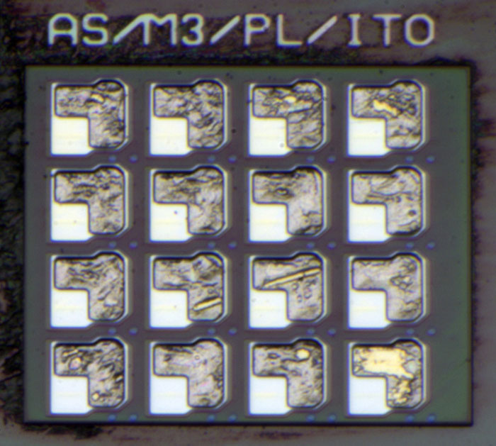
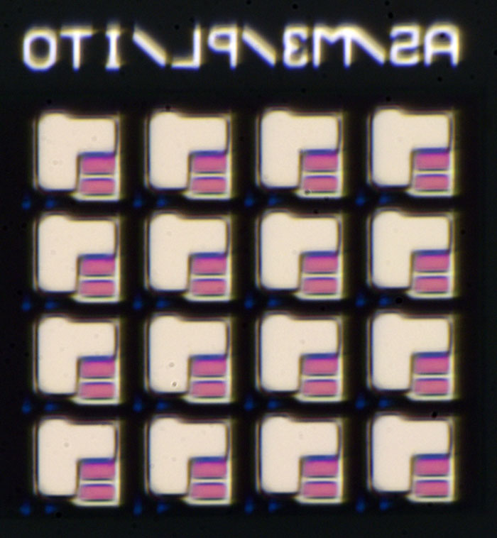
Here we see the uppermost metal layer M3. There is a lower part which increases the capacitance of the capacitor underneath. The capacitance is located between M2 and M1/M3.
The amorphous silicon looks reddish here.
Where the control lines cross each other there are blue dots. Perhaps these dots control whether or not the control lines have contact to each other.
 https://www.richis-lab.de/eink01.htm


