Author Topic: Optoelectronics - die pictures  (Read 18492 times)

0 Members and 1 Guest are viewing this topic.

Offline NoopyTopic starter

  • Super Contributor
  • ***
  • Posts: 1731
  • Country: de
    • Richis-Lab
Re: Optoelectronics - die pictures
« Reply #50 on: December 14, 2022, 04:31:00 am »


With the 5082-7300 Hewlett Packard produced a digit display which, due to its larger number of leds, allows a somewhat more natural image than a 7-segment display. The devices were produced at least until 1999, since there is a datasheet from Agilent and Agilent was spun off from Hewlett Packard in 1999.


The above block diagram is taken from the datasheet and shows how the display works. The 5082-7300 has a BCD interface and a latch. It provides a decimal point to the right of the number. Parallel to this, the 5082-7302 was available, which displays the decimal point to the left of the number. The third variant 5082-7340 has no decimal point at all. The input freed there makes it possible to switch off the complete display. While the 5082-7300 and the 5082-7302 just shows numbers and a minus sign (and a test pattern), the 5082-7340 is a hexadecimal display.


The red colored, but otherwise transparent housing allows a closer look at the circuitry without further processing. The control IC is clearly visible in the lower area. Above it are 20 LEDs, which are grouped into 13 segments. In addition, there is the decimal point.


The image quality is almost sufficient to analyze the circuit of the control IC in more detail.


The LEDs are easy to recognize too. The continuing bond connection is particularly interesting. According to the optical appearance, the bondwire was pressed onto the die and from there led directly to the next contact.

In this picture, one could think that it is a MESA structure, but it will be shown that this is not the case.


A simple way to expose the circuit is to thermally decompose the case. This reveals that the circuit itself is protected by a silicone-like potting and the red plastic is merely a cover.


In detail you can see that some bond joints have come loose. Bonded joints are not mechanically overly stable, yet the number of loosened wires is surprising, while otherwise hardly any mechanical impact can be seen.


The LEDs have an edge length of 0,45mm. The metal layer is designed to cover as little area as possible and thus remain as translucent as possible.


The dimensions of the control IC are 2,1mm x 2,0mm.


There is an hp logo on the lower edge of the die. A173B could be an internal project designation.


On the upper edge (image is rotated 180°) are five different squares, which probably served to monitor the manufacturing process. In the right corner are some numbers that look similar to the squares and so probably document the masks used. Clearly visible are the numbers 2, 3, 4 and 5. The remains below the 5 should probably represent a 6 and stand for the metal layer. This is plausible as far as it goes, since the metal layer often cannot be structured as precisely as the other areas. Above the 2, there could still be a 1.


 :-//


The individual circuit parts can be easily identified. The evaluation of the latch enable input is located in the lower area of the die (orange). It controls the five latches (yellow) which store the data of the BCD interface and the decimal point.

Each buffer passes the input signal normally and complementary to the first decoder matrix (blue), which generates control signals for 16 characters. Another decoder matrix (green) takes over the control signals and activates the LEDs representing the desired character. The upper decoder seems to be built in I2L technology, as described in more detail in the CA3161 (https://www.richis-lab.de/logic22.htm).

On the outside there are 14 output stages (red), which are controlled by the upper decoder matrix and activate the necessary LEDs. In the lower left corner is a circuit with a relatively large capacitor (purple). Apparently this is used to set the current through the output stages and thus through the LEDs. The left two bondpads in the bottom row are probably used to set this current. One of the bondpads is connected to Vcc in this device, the other one remained open. The potential that controls the current through the output stage transistors is fed to a bondpad in the lower right corner of the die, which most likely can be used for blanking.

It is quite possible that this integrated circuit was also used to drive the 5082-7340. This is supported by the blanking function and the fact that the decoders are designed to display 16 characters, although the 5082-7300 can just display 12 characters (0-9, minus and "all elements"). For the 5082-7340, however, the decoder must then be adapted to the different character set.


https://www.richis-lab.de/Opto15.htm

 :-/O
« Last Edit: December 14, 2022, 01:47:43 pm by Noopy »
 
The following users thanked this post: edavid, RoGeorge, ch_scr

Online David Hess

  • Super Contributor
  • ***
  • Posts: 16613
  • Country: us
  • DavidH
Re: Optoelectronics - die pictures
« Reply #51 on: December 14, 2022, 05:42:36 am »
I remember seeing those in the selection guides, and I have the HP databook for them somewhere, but they were always too expensive to use.
 

Offline RoGeorge

  • Super Contributor
  • ***
  • Posts: 6202
  • Country: ro
Re: Optoelectronics - die pictures
« Reply #52 on: December 28, 2022, 02:09:12 pm »
Are there any photos with decapped receiver ICs for consumer IR remotes, the ones with 3 pins V+, GND and digital Output like the TSOP or TFM series?  https://www.datasheetarchive.com/pdf/download.php?id=acce405bdd62e21b56baae28844e8f659b2c21&type=P&term=TFM%25201380%2520T%2520infrared%2520receivers

At a closer look it seems that there were 6 terminals out of which 3 were cut out, as seen in the attached photo.

Asking because I've read some have a PIN fotodiode, and the block diagram shows an integrated transimpedance amplifier.  Would be great if the analog signal would be accessible, so the IC could be use as an analog PIN detector.
« Last Edit: December 28, 2022, 02:16:18 pm by RoGeorge »
 

Offline NoopyTopic starter

  • Super Contributor
  • ***
  • Posts: 1731
  • Country: de
    • Richis-Lab
Re: Optoelectronics - die pictures
« Reply #53 on: December 28, 2022, 07:21:41 pm »
I don´t know such pictures.
We should take a closer look!  :-/O
 
The following users thanked this post: RoGeorge

Offline NoopyTopic starter

  • Super Contributor
  • ***
  • Posts: 1731
  • Country: de
    • Richis-Lab
Re: Optoelectronics - die pictures
« Reply #54 on: April 06, 2023, 06:54:47 pm »


The VQ130 built by the "Werk für Fernsehelektronik Berlin" is an IR-LED designed to transmit data via optical fibers. A typical receiver is the SP104 photodiode. According to the datasheet, the VQ130 can be operated with up to 300mA. A radiation power of up to 130µW is emitted. The emitted wavelengths range between 820nm and 870nm.


The datasheet contains a drawing of the complete module. The LED is located in a round housing that can be screwed into a heatsink. Besides the GaAs LED the VQ130 also contains a Si photodiode for monitoring the current beam power. For this reason, the module has four pins. A piece of optical fiber is integrated into the housing, which leads to an optical fiber connector.


The housing is constructed in two parts. Onto the lower element a cylinder is glued, which resembles a screw, and the optical waveguide is crimped into a thinner cylinder at the end.

The screw-shaped part is hollow and leads the pins to the outside. A potting protects the leads and seals the housing.


As specified in the datasheet, markings are stamped on the side. The W could stand for the manufacturer, whereas the "Werk für Fernsehelektronik" usually used the letters WF as an abbreviation. The meaning of the numbers 1421 remains unclear.


The end of the optical fiber is equipped with a screw connection.


There are some characters on the connector whose meaning remains unclear. The department standard TGL55141/01 specifies fiber optic cables and their designations. However, these designations do not seem to match the present character string. The datasheet of the VQ130 refers to the standard TGL55141/02, but this cannot be found.

VD could stand for a December 1987 production.


Removing the cylinder reveals that the connection pins lead to a round module that carries the photodiode. The connection to the LED, which is still in the cylinder, is torn off when it is opened.


A larger, round metal part that remains in the cylinder carries the LED. The cathode potential of the transmitter is led via two bondwires connected in parallel to a ceramic block and from there to the LED.

The round metal element was apparently connected to the lower part of the VQ130 just by some kind of glue. During assembly, the cylinder was probably put over as a last part, so it was possible to create the bond connections between the lower part and the carrier of the LED beforehand. Although most of the elements were only glued together, the electrical resistance of these connections seems to be low enough to use them as conductors to the LED's anode.


The photodiode is located on a ceramic carrier and is thus electrically isolated from the LED. The cathode potential is led to the ceramic carrier by two bondwires.

On the right pin, you can still see the remains of the two bondwires that connected the LED.


The edge length of the photodiode is 1,2mm.


There is some dirt and damage on the surface of the photodiode.


The bondwires that feed the LED's cathode potential from the ceramic block have both come loose from the semiconductor.


The detail clearly shows that the bondwires were pressed onto the die, but then came loose again.


The cylindrical upper part of the VQ130 is only slightly glued to the casing and can be easily removed from it after the optical fiber has been cut off. It can be seen that the carrier structure consists of two parts. The optical waveguide passes through a hole in the larger element and is glued there. The LED is located on a semi-circular disk, which is just glued to the upper element. It could be that this bisection served to align the LED with the optical waveguide.


The optical waveguide runs centrally through the cylindrical structure and ends in a trench, where it is fixed with a kind of clear potting. Inside the potting, the contours of the optical waveguide are no longer visible. The diameter of the optical waveguide is approximately 130µm. A standard value would be 125µm. Measurement tolerances could be the reason for this difference. The core of such an optical fiber usually had a diameter of 66µm or 50µm.


There is a sphere at the end of the optical waveguide. The slightly dark coloration in this area suggests that the sphere was glued on. The geometry probably optimizes the coupling of the light emitted by the semiconductor.

The dimensions of the LED are 0,40mm x 0,19mm. In the lower right corner you can see a crack. In the center, the die is discolored. Maybe the semiconductor was overloaded. It could be that at some point the left bondwire came loose, resulting in a current concentration on the right side that ultimately destroyed the structures.


The front side, where the light couples into the optical waveguide, is very smooth. The lateral radiation over a very smooth surface would be typical for a laser diode. It could be that diodes were used here whose quality was not sufficient to be able to operate them as laser diodes.

The upper edges at the short sides of the die are beveled. Presumably, this shape resulted from separating or reworking the lateral surfaces. Where the optical waveguide faces the die, one thinks one can detect a disturbance, an impurity or damage.


Here, the damage on the die can be seen even more clearly. While the left bondwire has apparently only come loose, the right contact surface is more severely damaged. This supports the theory that the left bondwire came loose first and then the LED was damaged by the local overload, which ultimately caused the right bondwire to come loose as well.


https://www.richis-lab.de/Opto16.htm

 :-/O
 
The following users thanked this post: _Wim_, RoGeorge, ch_scr

Offline NoopyTopic starter

  • Super Contributor
  • ***
  • Posts: 1731
  • Country: de
    • Richis-Lab
Re: Optoelectronics - die pictures
« Reply #55 on: April 09, 2023, 06:56:06 pm »


The VQ150 is an infrared laser diode that can be used in data transmission links with optical fibres. The manufacturer is the Werk für Fernsehelektronik Berlin. However, experts suspect that only the final assembly took place at the Werk für Fernsehelektronik and that the production of the laser diodes itself took place at the ZIE (Zentralinstitut für Elektronenphysik).

The VQ150 was presented at the Leipzig Spring Fair in 1987, but apparently could not be ordered for a long time. The model in the picture above bears the date 13.05.1991. Fittingly, the former "Volkseigener Betrieb" had already changed into a "GmbH" (limited liability company).

The wavelength of the VQ150 is between 820nm and 860nm, with a bandwidth of 1nm to 4nm. At 190mA, the laser diode emits a power of 2mW (3mW peak). The threshold voltage at which the laser effect starts is between 60mA and 120mA. The switching times are specified with a maximum of 1ns. Typical for laser diodes is the low permissible reverse voltage of just 1V. Laser diodes are also very sensitive to electrostatic discharges.


In the following, another VQ150 is analysed. On this model, the designation is not engraved into the casing, but is printed in black.


The "Fachbereichstandard" TGL42942, which describes the characteristics of the VQ150, includes the above drawing. A photodiode monitors the light output of the laser diode. A Peltier element keeps the laser diode at an optimal temperature. A thermistor can be used to create a control loop. Temperature fluctuations would influence both the wavelength and the efficiency of the laser diode.


The VQ150 is equipped with a piece of optical fibre that ends in a connector.


The characters printed on the shrink tubing of the fibre optic connector apparently belong to the designation of the fibre optic cable. According to the "Fachbereichstandard" for the VQ150, the full designation of the fibre optic cable is "LWL-VK NRÜ 131 EBS-GO 3006 4112".

W9 presumably stands for production in September 1988.


The VQ150 has a gold-plated housing. The number 3524 is stamped on the side, a consecutive number according to the "Fachbereichstandard".


The cover and the sleeve of the fibre optic cable are welded to the housing. However, the welding of the sleeve was not completed.

The sleeve has two holes on the top, which were certainly used to fix the optical fibre and seal the system.


When the case is opened, a golden layer comes off the surface, which appears silver on the back. It is interesting that the case underneath is gold-coloured again.


[...]

 :-/O
 
The following users thanked this post: doktor pyta, _Wim_, RoGeorge, ch_scr

Offline NoopyTopic starter

  • Super Contributor
  • ***
  • Posts: 1731
  • Country: de
    • Richis-Lab
Re: Optoelectronics - die pictures
« Reply #56 on: April 09, 2023, 06:57:09 pm »


The wiring shows that the production involved a lot of manual work.


In the "Industriesalon Schöneweide" (https://www.industriesalon.de), a display board shows the manufacturing steps in the production of a VQ150. The individual elements can be easily identified in this module.


Even if it does not appear so at first glance, the construction is quite clear. The optical waveguide is fed into the housing from the right through a sleeve. The laser diode is located where the optical waveguide ends. Behind it is the photodiode. On the far left, the Peltier element ensures a constant temperature. To the right of the laser diode is the associated thermistor.


There are some splashes of solder in the casing.


The optical fibre is guided into the housing through a sleeve. A nickel tube protects the glass fibre.


The optical elements are fixed on a module, which is called "Aufnahme" on the WF display board. The "Aufnahme" carries the photodiode and has a notch into which the tube with the optical fibre is inserted and soldered.

In a space between the photodiode and the glass fibre, the so-called "Träger" is inserted, on which the laser diode is located. The "Träger" seems to have been glued. Probably the laser was aligned with the glass fibre.

On the "Träger", next to the WF logo, are the numbers 03377. Presumably, the sequence of numbers serves to trace the laser module.


Since the laser light emerges from the laser diode on both sides, the photodiode can be arranged opposite the optical waveguide and thus the currently emitted light power can be determined.

With respect to the laser diode, the photodiode is slightly rotated around both the vertical and horizontal axes. This measure ensures that light reflected from the photodiode does not hit the laser diode or the optical waveguide.


The laser diode is placed on a carrier which, according to the diagram, consists of silicon. While the laser diode is based on GaAs according to the datasheet, the diagram specifies AlGaAs as base material. Usually, laser diodes are produced with both materials. The different bandgaps are used to build the structures necessary for a laser.


The dimensions of the laser diode are 0,40mm x 0,20mm. The current flows through the semiconductor from the bottom to the top. It is a classic edge emitter in which the laser light is emitted via the side surfaces. These side surfaces are correspondingly smooth.

The upper edges on the short sides of the die are bevelled. The bondpads contain notches. The same component seems to have been used as in the IR-LED VQ130, which supports the theory that laser diodes of insufficient quality were used as normal IR-LEDs.

The diameter of the glass fibre can be determined to be approximately 0,13mm. While in the IR-LED VQ130 a kind of sphere was placed at the end of the glass fibre, in the VQ150 it was left pointed. But the end is still rounded. As with the VQ130, the last piece seems a little darker, as if it had been treated with some kind of varnish.

The distance between the laser diode and the glass fibre is just 10µm.


The photodiode is located on a ceramic carrier on the so-called "Aufnahme". The upper potential is supplied with two bondwires.


The Peltier element connects the "Aufnahme" to the area of the enclosure that must be screwed to a heatsink. In this way, the heat generated can be dissipated as efficiently as possible. Since the "Aufnahme" does not otherwise touch the enclosure, it is relatively well insulated thermally. The datasheet specifies 4V and 0,75A as maximum values for the Peltier element.


The Peltier element shows the typical structure. There are differently doped semiconductor cuboids between two white ceramic plates. Depending on the doping, the current is allowed to flow through the cuboids from one direction or the other. The different energy levels between the semiconductor and the contacting metal lead to heat emission on one side and heat absorption, i.e. cooling, on the other side.


The red thermistor is glued into a large bulge of the "Aufnahme" opposite the Peltier element.


https://www.richis-lab.de/Opto17.htm

 :-/O
 
The following users thanked this post: Vgkid, RoGeorge, ch_scr

Offline NoopyTopic starter

  • Super Contributor
  • ***
  • Posts: 1731
  • Country: de
    • Richis-Lab
Re: Optoelectronics - die pictures
« Reply #57 on: April 26, 2023, 07:53:01 pm »


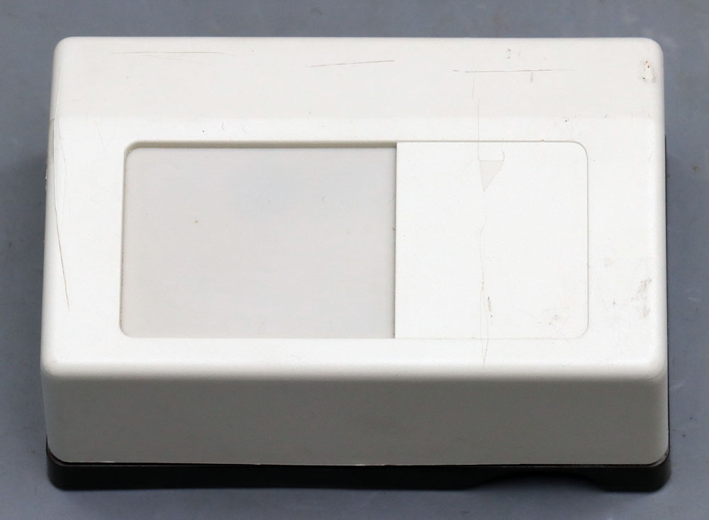
The IR 6 is a passive infrared motion detector from Telenorma. It requires a supply voltage between 10,5V and 15V. In addition to the alarm output, the IR 6 offers tamper protection, where a control loop is interrupted when you open the housing. On the front side there is only an inconspicuous white window transparent to infrared radiation.
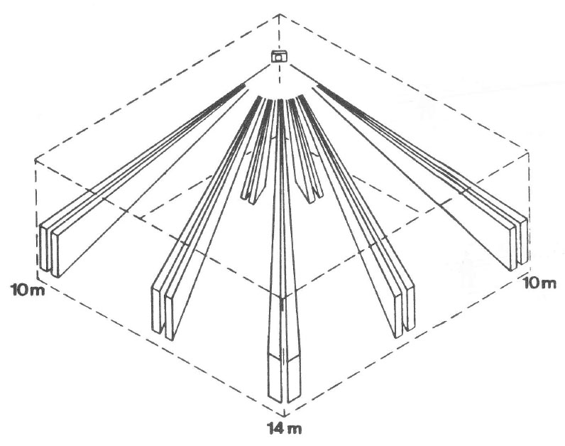


The datasheet shows the detection ranges of the sensor. Five areas extend in the horizontal plane over an opening angle of 90°. The range depends on the angle at which the sensor is mounted on the wall and is up to 14m. At close range, the IR 6 has two additional detection zones.
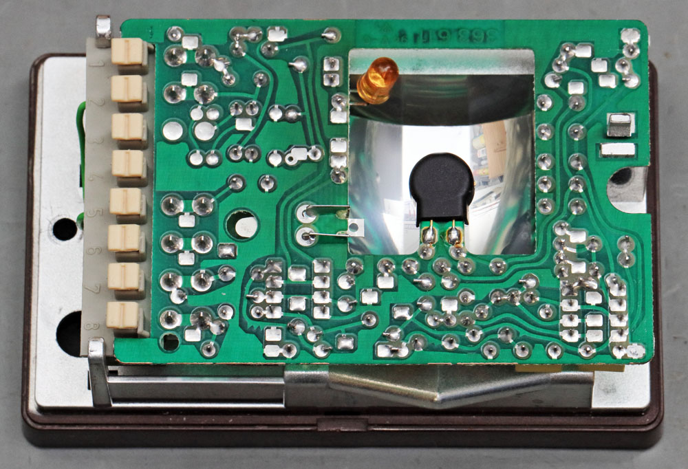


If you remove the cover, you can see the back of a circuit board. The module has been rotated by 180° here. The contact strip is on the left, and a window on the right provides an entry point for infrared radiation. The tamper protection is located in between. A pin fixed in the cover presses there through a hole in the board onto a metal part which closes the loop of the tamper protection.

The orange LED is a so-called walk test indicator. According to the datasheet, it is not visible through the housing, but can also be unplugged. This ensures that no unauthorized person can test the detection range.
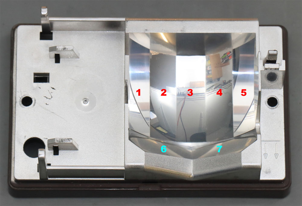


Infrared sensors for motion detectors usually offer very few, usually only two elements. The desired resolution over a large area is achieved using Fresnel lenses or concave mirrors. These optical elements ensure that the irradiation on the sensor changes relatively strongly, even if only a small heat source moves through the room.

If the circuit board is removed, the concave mirror becomes visible, which in the case of IR 6 directs the incoming infrared radiation to the sensor and thus defines the detection areas. Areas 1-5 are the more far-reaching zones. Surfaces 6 and 7 collect the infrared radiation from the near range.
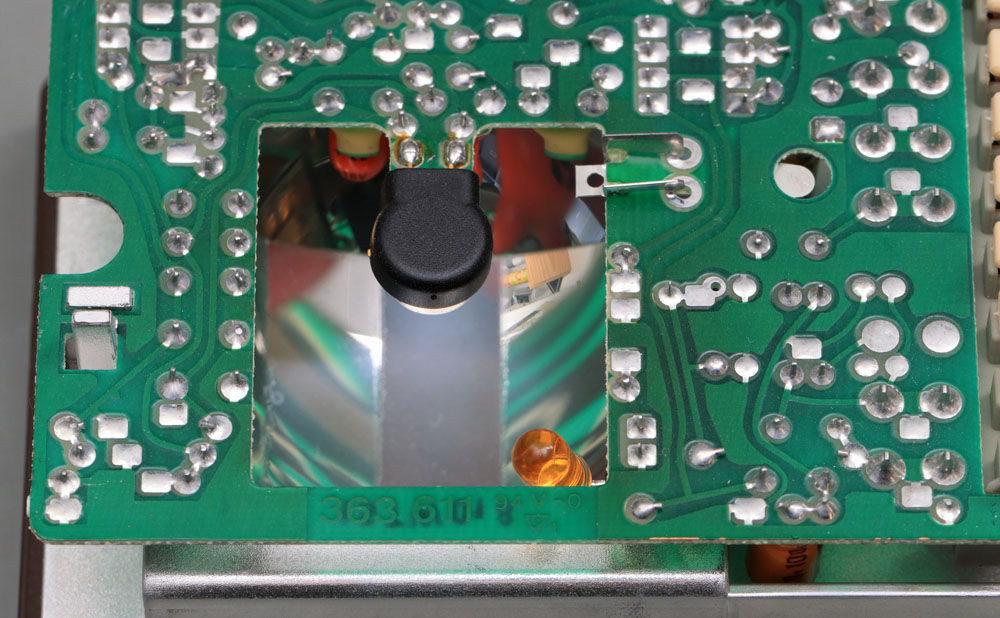


Turned by 180° again, the transition from the wide-range to the close-range reflectors can be clearly seen through the cutout in the pcb. The actual sensor is located under the black element.
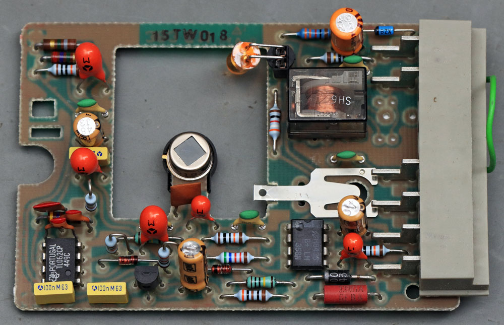


The circuit is not too complex. Usually the signals of the sensor are actively filtered and amplified. Approximately in the center you can see the metal element of the tamper protection and above it the relay that switches the output of the motion detector.
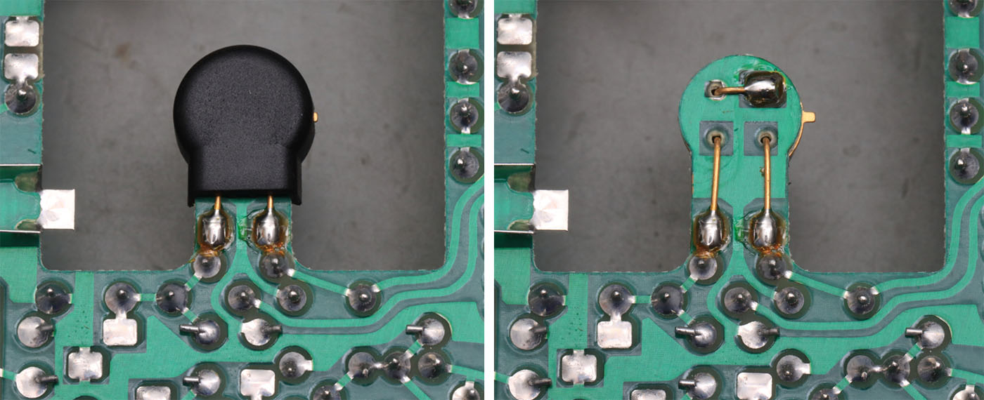


The sensor is covered with a plastic element on the back. Perhaps this ensures that no infrared radiation falls on the pins and generates inhomogeneous heating. Such sensors are extremely sensitive and it is quite conceivable that an inhomogeneous heating of the pins already generates a problematic interference signal.

The sensor lies directly on the circuit board. However, you must not heat the sensor elements too much. The datasheet recommends to leave the pins at least 6,35mm long. This explains why the pins are bent downwards and soldered further away of the sensor.
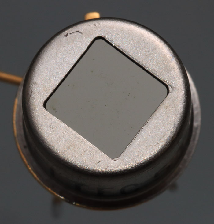


On the front side there is a square window with a filter element.
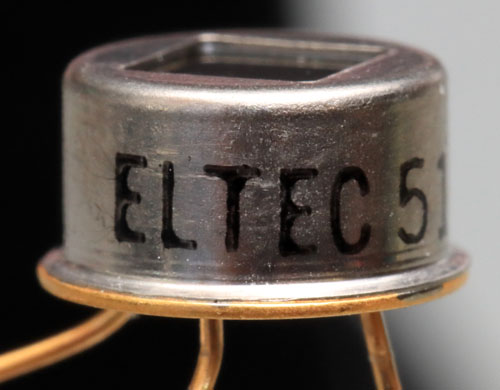


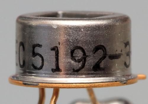
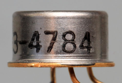
The labeling on the side shows that it is the Dual IR detector 5192 from Eltec. The number 3 behind the designation shows which filter is located in front of the sensor. 3 stands for the silicon filter, which allows wavelengths between 6µm and 25µm to pass. A total of 35 different filters are available. 4784 seems to be a date code.
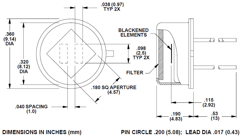


The datasheet shows that there are two sensor elements in the housing.
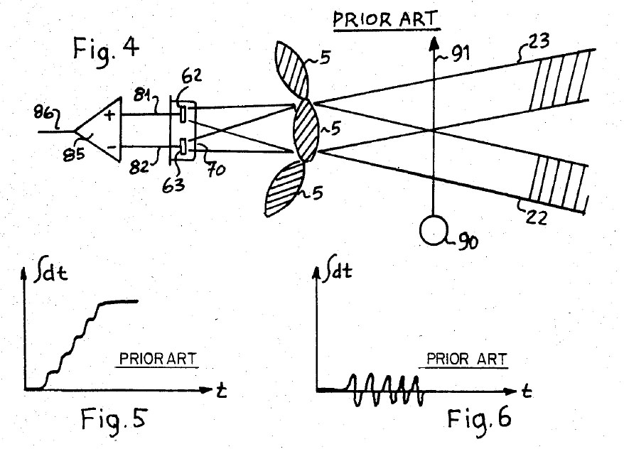


In the datasheet, reference is made to patent US4523095, whose illustrations make it easier to understand how the sensor works. If only a single pyroelectric element were used as a sensor, a warm body in the detection range would just cause the output signal to increase (Fig. 5).

In contrast, the arrangement and interconnection of two pyroelectric elements and the evaluation via a differential amplifier results in an oscillating signal when passing through the detection areas (Fig. 6). This signal is easier to evaluate.
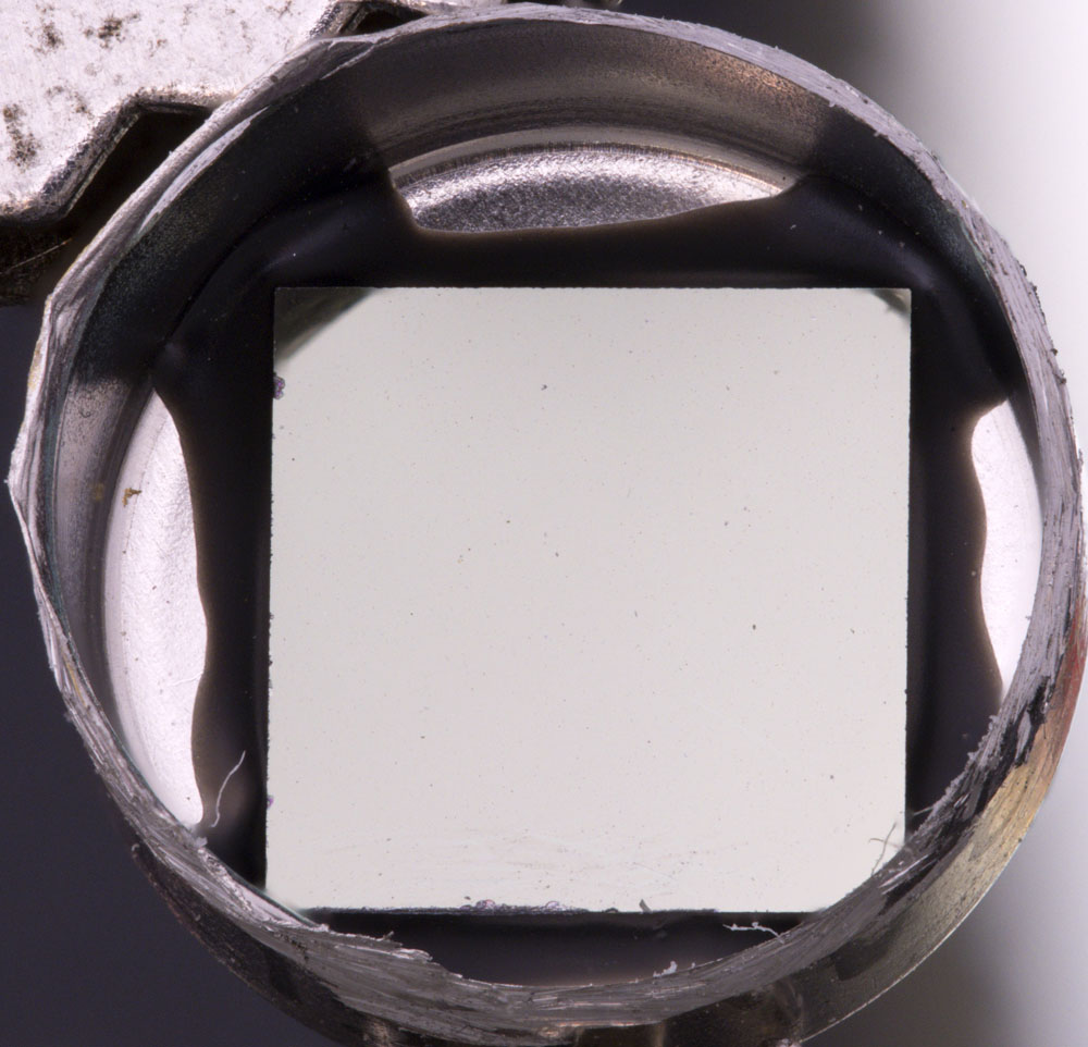


If you open the housing, you can take a look at the glued-in filter element.
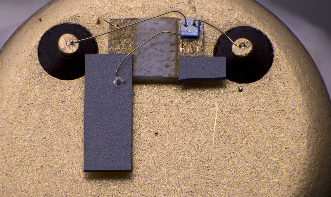


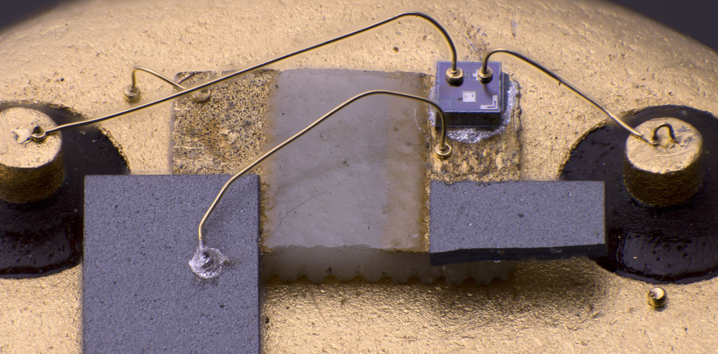
The two pyroelectric elements are mounted on a ceramic carrier. It can be seen that the right element is broken off. The damage could have occurred when opening the case. However, the module in question was discarded because its functionality was unreliable. This suggests that the element had already broken off before.
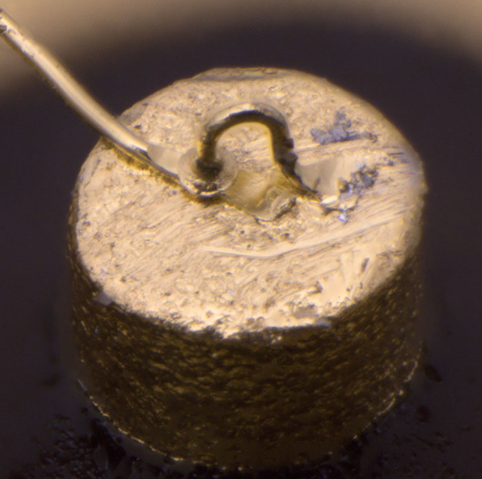


So-called security bonds were used on the connecting pins. A ball bond is supposed to secure the wedge bond.
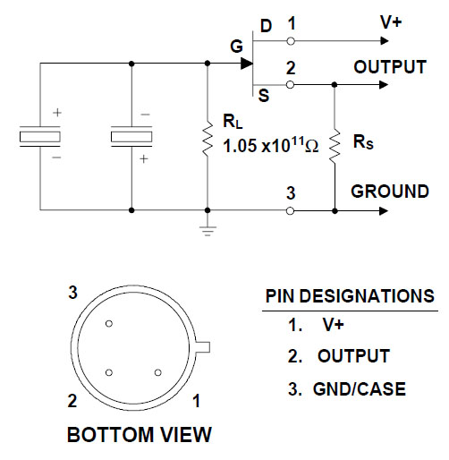


The datasheet shows how the sensor works. The two pyroelectric elements are connected antiparallel and are guided to the gate of a JFET. This interconnection ensures that when an infrared beam changes from one element to the other, the polarity of the signal is reversed. The JFET represents the differential amplifier shown in the patent above. The value of the resistor R_L is extremely high at 105GΩ. Such a high value is necessary because the pyroelectric elements have a very high internal resistance.
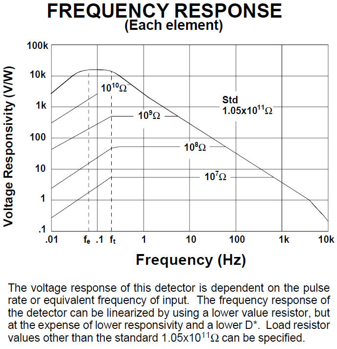


It seems that the sensor can be obtained with lower resistance values. Since R_L discharges the capacity of the sensor, a lower value has a positive effect on the bandwidth. At the same time, however, the sensitivity is reduced.
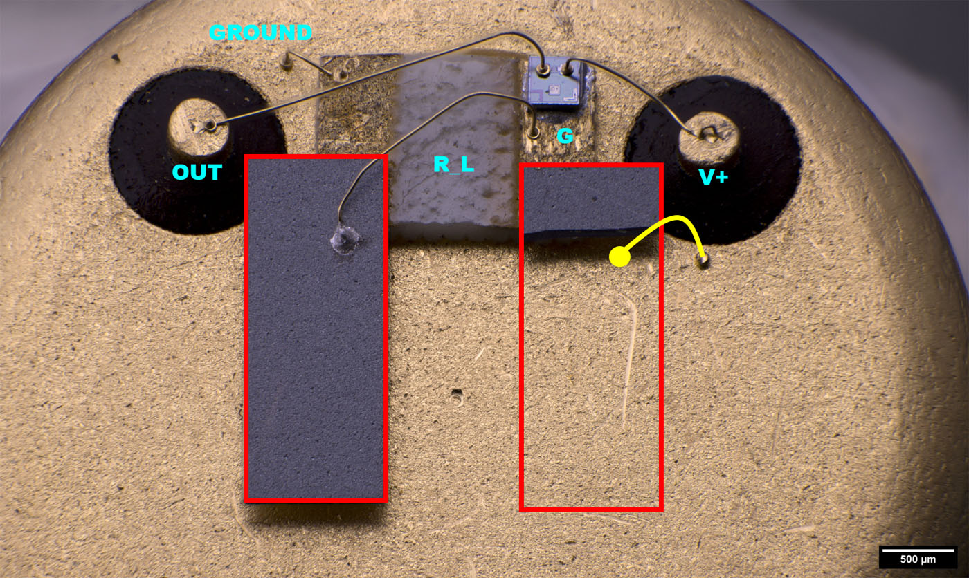


With the background of the operation one can interpret and extrapolate the structures. On the left pyroelectric element, the top is connected to the gate of the JFET. On the right element, the bottom side is directly connected to the gate potential due to the attachment. It can be assumed that the top was connected to the rest of the ball bond on the right of the element (yellow). The extremely high resistance thick film resistor is applied to the ceramic support between the gold contacts.

The significance of the imprint between the thermoelectric elements remains open. It does not appear to be a proper wedge bond. It also lacks the security bond. This suggests that it was not a functional element. Perhaps it is a remnant of the manufacturing process.
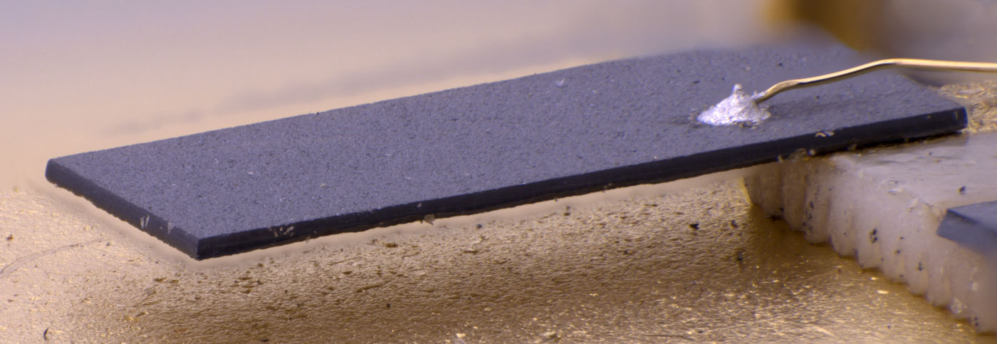


Pyroelectric elements can be manufactured from different materials. On Eltec's website, only lithium tantalate is ever mentioned.
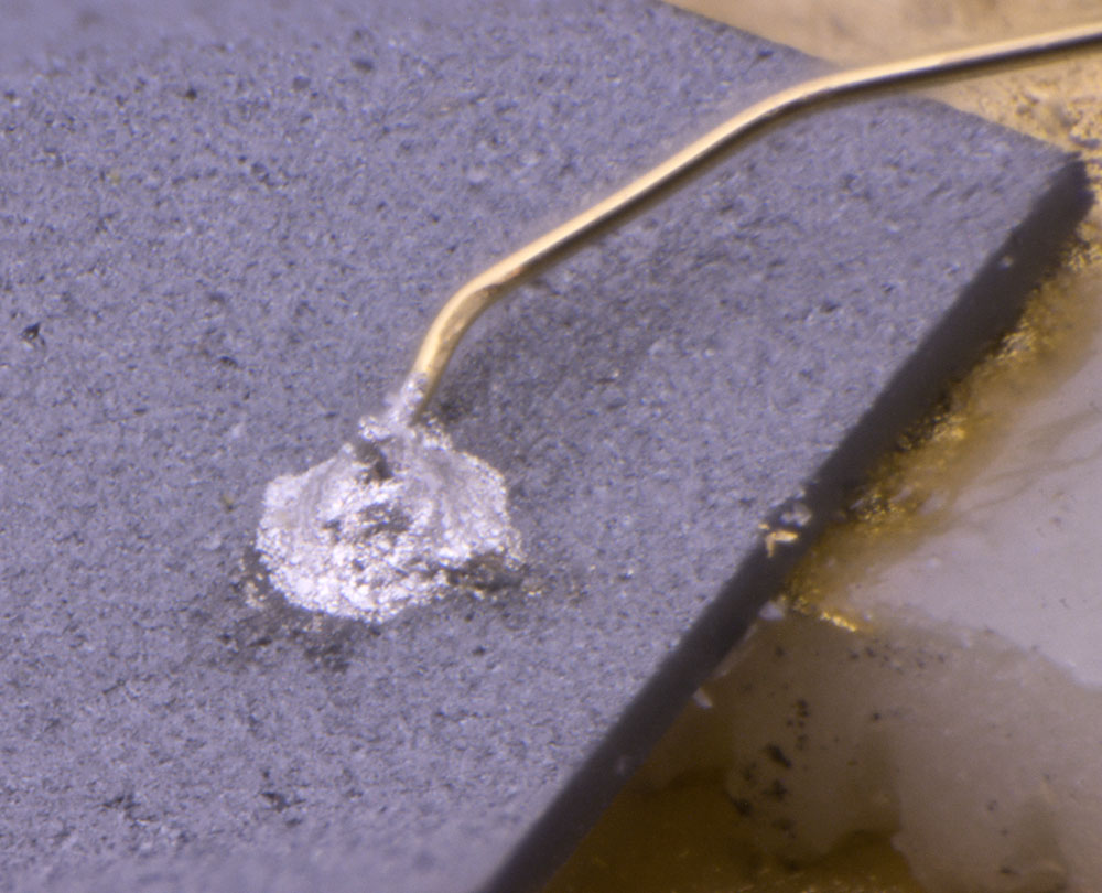


Since it was not possible to bond on the pyroelectric material, the bondwire was soldered.
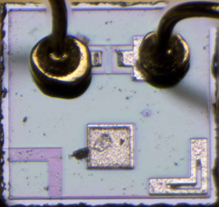


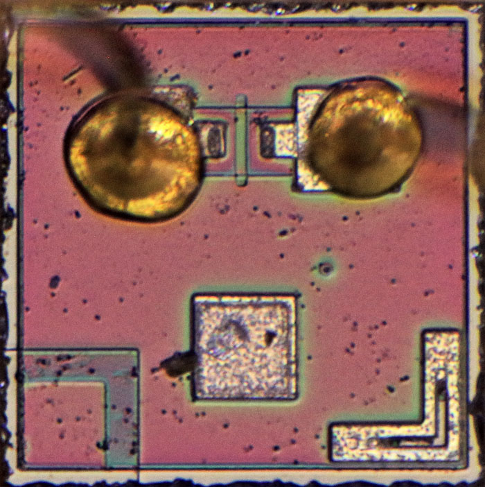
The edge length of the JFET is 0,35mm. The mode of operation can be seen clearly. The two adjacent bondpads contact a wide n-doped strip, which is located in a p-doped area. A thin p-doped strip is deposited on the wide strip, forming an n-doped channel surrounded by p-doped regions over its complete circumference.

Inside the sensor, the gate potential is supplied from below through the substrate. The free bondpad in the lower area offers the possibility to supply the gate potential alternatively via a bondwire.


https://www.richis-lab.de/Opto18.htm

 :-/O
 
The following users thanked this post: doktor pyta, _Wim_, RoGeorge, ch_scr, iMo

Offline RoGeorge

  • Super Contributor
  • ***
  • Posts: 6202
  • Country: ro
Re: Optoelectronics - die pictures
« Reply #58 on: April 26, 2023, 09:51:00 pm »
Thanks, never seen one opened before!  :-+

Mythbusters, the TV show, have had an episode about how to defeat IR alarms.  IIRC, by putting a sheet of glass in front of the sensor, or by crossing the room while keeping a bed-sheet towards the sensor and hiding behind it, was possible to become IR invisible for the sensor.
 
The following users thanked this post: MegaVolt

Offline NoopyTopic starter

  • Super Contributor
  • ***
  • Posts: 1731
  • Country: de
    • Richis-Lab
Re: Optoelectronics - die pictures
« Reply #59 on: April 27, 2023, 03:45:58 am »
 :-+

I heard it should be possible to defeat these IR sensors with styrofoam too.

Looking through a thermal camera it is suprising for me that such camouflage is able to defeat IR sensors.
All these methods show a uniform temperature. However in a room there are a lot of parts looking very different, in infrared too. So if you put a bed-sheet over these parts the IR picture is changing and the sensor should recognize that.  :-//

Offline bookaboo

  • Frequent Contributor
  • **
  • Posts: 728
  • Country: ie
Re: Optoelectronics - die pictures
« Reply #60 on: April 27, 2023, 05:28:17 am »
Fascinating images.

How easily a PIR sensor can be beaten depends more on the amplifier and comparator stages than the element itself. Simple gain adjustment changes the sensitivity, with the obvious trade off that you can get false detects. With some processing in place of a simple comparator it's possible to get significant improvement, though getting the lens right is the real key.
 
The following users thanked this post: Noopy

Offline RoGeorge

  • Super Contributor
  • ***
  • Posts: 6202
  • Country: ro
Re: Optoelectronics - die pictures
« Reply #61 on: April 27, 2023, 10:49:39 am »
The weirdest thing is how they atached the wire to the pyroelectric material.  ???

The pyroelement looks porous and not solder friendly.  Combined with the extra measures required to avoid heat while mounting the entire sensor to the PCB, my best guess is the internal bonding to the pyroelements was made with some sort of conductive glue.  Wouldn't be surprised if that would be a glue that soften and melt at small temperatures, and thus the extra care when mounting the sensor.  These are only speculations, no idea how it really is.

Anybody knows any details about bonding the wires to the pyroelectric material?

Offline rteodor

  • Regular Contributor
  • *
  • Posts: 122
  • Country: ro
Re: Optoelectronics - die pictures
« Reply #62 on: April 27, 2023, 11:25:25 am »
Thanks, never seen one opened before!  :-+

Mythbusters, the TV show, have had an episode about how to defeat IR alarms.  IIRC, by putting a sheet of glass in front of the sensor, or by crossing the room while keeping a bed-sheet towards the sensor and hiding behind it, was possible to become IR invisible for the sensor.

If my memory is right they tested two types of sensors: IR and ultrasound. For the IR it was possible to defeat them by moving very slowly and the bed-sheet was somewhat successful against the ultrasound sensors.
 
The following users thanked this post: RoGeorge

Offline NoopyTopic starter

  • Super Contributor
  • ***
  • Posts: 1731
  • Country: de
    • Richis-Lab
Re: Optoelectronics - die pictures
« Reply #63 on: April 27, 2023, 06:20:28 pm »
A small update to the VQ150:


The magazine "Nachrichtentechnik Elektronik" (issue 5, 1989) contains an article about the VQ150. In it, one possible application is the fiber optic transmitter board of the DÜS-LL-34 system. 480 telephone connections can be transmitted simultaneously via the DÜS-LL-34. With 11 repeaters transmission distances up to 120km are possible. The datarates here are 34MBit/s. Theoretically, up to 167MBit/s should be achievable with the VQ150.


The above mentioned magazine "Nachrichtentechnik Elektronik" contains a circuit diagram which shows how a circuit around the VQ150 can look like.

In the upper part is the temperature control, which is monitored to the right with a comparator. The current through the laser diode is made up of two parts. The circuit in the lower section provides a certain base current, which always flows through the laser diode. The digital signal on the left passes through a differential amplifier and then causes the current through the laser diode to increase, resulting in a laser pulse. If the input signal fails, which is relatively evenly distributed, then a circuit ensures that the idle current is also switched off. This prevents the laser diode from aging unnecessarily. Another comparator activates the alarm output when the idle current fails.


And here we see a side view of the architecture.


https://www.richis-lab.de/Opto17.htm

 :-/O

Offline NoopyTopic starter

  • Super Contributor
  • ***
  • Posts: 1731
  • Country: de
    • Richis-Lab
Re: Optoelectronics - die pictures
« Reply #64 on: June 04, 2023, 07:31:57 pm »


The component shown here is from the DT8380 infrared thermometer (https://www.richis-lab.de/DT8380.htm). It is a so-called thermopile. The window on the upper side is transparent for infrared radiation. Inside is a series connection of thermocouples, which generate a voltage proportional to the thermal radiation.

The housing does not bear any labeling. The designation of the component remains unclear, as does the manufacturer.


A cuboid glued into the lid of the housing represents the optical window.


Inside the case is a large die that represents the thermopile. It is connected to two pins via two bondwires.


A thermistor allows to meassure the reference temperature of the thermopile.


The article "Design and Fabrication of a Low-Cost Thermopile Infrared Detector" published in the journal Micromachines shows the structure of such a thermopile. The active part is located above a large cavity. This construction method is the reason why such thermopiles belong to the MEMS family.

The so-called hot junctions are arranged around the inner circle. In this area, the contact points of two different materials form thermocouples. A thermoelectric voltage proportional to the temperature drops across them. The series connection of the thermocouples also results in thermocouples in the outer area, the so-called cold junctions. The outer thermocouples must be kept as close as possible to the reference temperature of the housing. For this reason, one tries to isolate the two areas as good as possible thermally from each other. The cavity ensures that just the thin wires are a relevant heat conductor.


If you choose a slightly different focus, you can see the bottom of the housing through the active area.


The edge length of the die on which the thermopile is integrated is 1,75mm. The character string OTP666C on the lower edge cannot be assigned to any sensor designation or manufacturer. The bonding areas in the lower corners are marked with - and +. The voltage of the thermopile can be tapped at these points.

The bondpads in the upper corners are connected with a long line that extends in many loops over the left, the right and the upper edge. Perhaps this is an option to determine the reference temperature of the thermopile. The integration of a heater seems to make little sense, but could possibly be useful in the context of a special adjustment.


The so-called hot junctions (red) are located in the center under the black coating. If the infrared radiation heats these junctions, a temperature voltage proportional to this temperature is generated. The series connection of 116 thermocouples results in a relatively high output voltage. The cold junctions (cyan) are arranged in a square around the cavity.


A black coating with an rough surface is applied to the inner area. This ensures that as much infrared radiation as possible is absorbed and increases the temperature of the inner area.

The outer optics of the DT8380 infrared thermometer reduces the risk of infrared radiation hitting the outer area of the thermopile and heating the cold junctions there, which would falsify the measurement.


The article mentioned above deals in more detail with the shape of the hot junctions, which are not visible in the present component due to the coating.


For each thermocouple, an on average ~20µm wide polysilicon strip leads to the inner contact. On top of the silicon strip is the corresponding aluminum strip, which is considerably narrower at about 4µm. In the edge area, the metal layer then contacts the next polysilicon line.

In the tilted image showing the coating it can be seen that the lines are much wider than they are high. It can therefore be estimated that the lines are just a few micrometers high.


https://www.richis-lab.de/Opto19.htm

 :-/O
 
The following users thanked this post: edavid, doktor pyta, _Wim_, Gyro, RoGeorge, ch_scr, magic

Offline RoGeorge

  • Super Contributor
  • ***
  • Posts: 6202
  • Country: ro
Re: Optoelectronics - die pictures
« Reply #65 on: June 04, 2023, 08:09:26 pm »
Wow, thanks!  I've become very curious about the inner structure after buying an infrared thermometer, the cheap one without thermal camera.  Very nice toy.

It's all fun measuring temperatures around, until you go outside and measure the temperature of the night sky...  :o

Offline NoopyTopic starter

  • Super Contributor
  • ***
  • Posts: 1731
  • Country: de
    • Richis-Lab
Re: Optoelectronics - die pictures
« Reply #66 on: June 04, 2023, 08:37:53 pm »
It was a pleassure!  :)

That´s one of those things everybody uses and just a few know what exactly is inside and how it works. I wasn´t aware of the structures either until I took these pictures and read some articles about thermopiles.

Offline T3sl4co1l

  • Super Contributor
  • ***
  • Posts: 21674
  • Country: us
  • Expert, Analog Electronics, PCB Layout, EMC
    • Seven Transistor Labs
Re: Optoelectronics - die pictures
« Reply #67 on: June 04, 2023, 09:09:38 pm »
Cool.  Saw a design some years ago using thermopiles for flame detection, don't remember the part numbers though.  Think they were a rectangular design.  Don't think they were cheap...

Tim
Seven Transistor Labs, LLC
Electronic design, from concept to prototype.
Bringing a project to life?  Send me a message!
 

Offline NoopyTopic starter

  • Super Contributor
  • ***
  • Posts: 1731
  • Country: de
    • Richis-Lab
Re: Optoelectronics - die pictures
« Reply #68 on: June 04, 2023, 09:33:53 pm »
Yes, there are different geometric shapes. I have seen rectangular designs too.

I assume if you can build MEMS structures than building such a thermopile is no big problem. Nevertheless it´s a MEMS structure and that is a special process with an appropriate price label.

Offline NoopyTopic starter

  • Super Contributor
  • ***
  • Posts: 1731
  • Country: de
    • Richis-Lab
Re: Optoelectronics - die pictures
« Reply #69 on: June 07, 2023, 08:29:36 pm »
I found the manufacturer of the thermopile:


Oriental System Technology, never heard of them...  ;D
This is the OTP638D2 but you can see the design is the same as in our thermopile.


https://www.richis-lab.de/Opto19.htm#OTP638D2

 :-/O
« Last Edit: June 07, 2023, 08:31:32 pm by Noopy »
 

Offline NoopyTopic starter

  • Super Contributor
  • ***
  • Posts: 1731
  • Country: de
    • Richis-Lab
Re: Optoelectronics - die pictures
« Reply #70 on: June 09, 2023, 07:12:47 pm »


Here you can see one of the many laser modules that just require a supply voltage and are used for simple marking tasks. The beam power is usually less than 1mW, so no protective measures are necessary when using it. A manufacturer cannot be identified. The present module is taken from the DT8380 infrared thermometer (https://www.richis-lab.de/DT8380.htm).

For a satisfactory and reliable function laser diodes need some electrical and optical auxiliary structures. For this reason, discrete laser diodes are not used for simple marking tasks, but ready to use modules like the one shown here.


The black shrink tubing at the rear end of the module protects a small pcb that adjusts the current through the laser diode. For this purpose, the current beam power is determined in the laser diode and regulated to a constant value.

Setting a constant current would not be sufficient because the beam power of a laser diode is strongly influenced by production fluctuations, temperature and aging. To make matters worse, if the current is set slightly too low, the laser threshold will not be reached and the laser diode will behave like a weak LED. If the current is set slightly too high, the laser diode will age very quickly and fail prematurely.

The specified beam power must never be exceeded for safety reasons. At the same time, optical power meters are often not at hand. This is another reason for setting the output power during production and and controlling it directly.


The circuit for power control is relatively simple. The transistor Q2 adjusts the current through the laser diode. Q2 is controlled by Q1. The photodiode is connected to the base of Q1. If the beam power increases, more current flows through the photodiode, Q1 is conducting more current, the base current of Q2 is reduced and so is the current through the laser diode.

MMBT3904 (https://www.richis-lab.de/BipolarA32.htm) were used as transistors. At the input of the circuit there is a 100nF capacitor, which ensures that the circuit works stable. Of course, this module is not suitable for fast modulation.


A lens can be seen in the hole on the front. On the back, you can already see that a component has been installed in a metal sleeve.


If you cut open the metal sleeve, the lens becomes visible in the front area. This is the so-called collimator. Laser light is strongly bundled, but it does have a certain divergence. Consequently, a laser beam also fans out with increasing distance. The collimator reduces the divergence so that the laser beam comes even closer to an ideal light beam.

A closer look reveals that the upper sleeve has a thread. One could probably have unscrewed this element, which was secured with adhesive. A spring fixes the lens in place. During manufacture, the optimum distance of the lens can be set by simply turning the sleeve.


You can already see the laser diode...


The laser diode is located in the lower sleeve. The designation laser diode is common, but does not quite do justice to the assembly, since the photodiode for power measurement is also located in the casing.

The relatively massive bottom allows efficient heat dissipation. This is important in some applications, since temperature fluctuations strongly influence efficiency and wavelength.


The laser diode is soldered on a thick vertical metal element. The laser is an edge emitter. The laser beam is coupled out at the upper edge. Part of the light also leaves the edge emitter at the bottom and is used to determine the optical power. For this purpose, a photodiode is located below the laser diode. The photodiode is mounted on a slope so that reflected light is not emitted to the outside.


The bondwire of the photodiode has a ball bond on one side. The corresponding wedge bond is located on the other side. The laser diode was basically connected in the same way, but here an additional ball bond was placed on the wedge bond to secure the connection. Such a measure is called a security bond. Apparently, the bond connection was somewhat more critical with the laser diode, so that the additional security became necessary.


The dimensions of the laser diode are 0,29mm x 0,25mm x 0,1mm. The die is located on a relatively thick carrier, which in turn was soldered onto the metal post of the housing.


The front edge of the die is very smooth so that the laser radiation is disturbed as little as possible. Two things are also noticeable. On the one hand, the die protrudes a bit beyond the carrier and on the other hand, the inactive edges are clearly slanted.


The surface of the lateral edges is very rough. This is nothing unusual, but material seems to have broken out especially in the center (on both sides).


Photodiode - nothing special...


https://www.richis-lab.de/Opto20.htm

 :-/O
 
The following users thanked this post: edavid, doktor pyta, TurboTom, RoGeorge, ch_scr, rteodor

Offline NoopyTopic starter

  • Super Contributor
  • ***
  • Posts: 1731
  • Country: de
    • Richis-Lab
Re: Optoelectronics - die pictures
« Reply #71 on: June 13, 2023, 06:12:36 pm »


A laser diode only provides laser light above a certain current. This so-called laser threshold can be determined by increasing the current through the laser diode and simultaneously observing the current generated in the photodiode. From 11mA, the light output and thus the photocurrent increases sharply. From here on, laser light is generated. Before that, lossy effects dominate, which strongly reduce the efficiency.


At a current of 1mA, well below the laser threshold, the laser diode already shines clearly.


At a current of 15mA, the laser diode shines much brighter and it becomes increasingly difficult to capture high quality images of it.


The active layer is located on the surface facing the carrier / heatspreader. This makes sense because the thermal conductivity of the semiconductor material is relatively poor. The shorter path from the active area to the package enables more efficient heat dissipation.


In operation, the partial metallization on the bottom side becomes more clearly visible. In the open areas on the right and left, a brightness level is formed in each case, which results from the beveled edges. The beam diameter is about 20µm. Even with a beam power of just 1mW, a power density of 250W/cm² results on this surface.


https://www.richis-lab.de/Opto20.htm#Laserschwelle


 :-/O
 
The following users thanked this post: RoGeorge

Offline PartialDischarge

  • Super Contributor
  • ***
  • Posts: 1611
  • Country: 00
Re: Optoelectronics - die pictures
« Reply #72 on: June 13, 2023, 06:19:06 pm »
"The photodiode is mounted on a slope so that reflected light is not emitted to the outside"
Not exactly, it is sloped to prevent reflections to the laser which will create amplitude oscillations, wavelength changes and changes in the modes.
 
The following users thanked this post: Noopy

Offline NoopyTopic starter

  • Super Contributor
  • ***
  • Posts: 1731
  • Country: de
    • Richis-Lab
Re: Optoelectronics - die pictures
« Reply #73 on: June 13, 2023, 06:23:16 pm »
"The photodiode is mounted on a slope so that reflected light is not emitted to the outside"
Not exactly, it is sloped to prevent reflections to the laser which will create amplitude oscillations, wavelength changes and changes in the modes.

Thanks for the correction!  :-+
« Last Edit: June 13, 2023, 06:27:37 pm by Noopy »
 

Offline NoopyTopic starter

  • Super Contributor
  • ***
  • Posts: 1731
  • Country: de
    • Richis-Lab
Re: Optoelectronics - die pictures
« Reply #74 on: July 25, 2023, 06:50:06 pm »


Here you can see the transmitter module of the Motorola Optobus system (https://www.richis-lab.de/transceiver03.htm). It has already been soldered from the pcb and then was reattached with hot glue to keep the optical impression to some extent. The housing is made of a translucent polymer and has six pins on both sides.


As the IEEE article "A Low-Cost High-Performance Optical Interconnect" clearly shows, the laser diodes are located outside the housing on the rear surface. The design does not seem optimal for power dissipating. However, the IEEE article describes that this disadvantage is not too great. The semiconductor material conducts heat relatively poorly, which is why the heat dissipation via the contacts is much more relevant.


In fact, the laser array is not one module, but two elements. The semiconductors are already badly damaged. In case of the receiver module, you can see that this area was originally protected with a silicone gel. Here, only the dirty remains of this gel are still visible.


There are two holes on the front. They serve to align the plug-in system. In addition, a fine structure can be seen running through the housing from left to right. This is a different polymer with a different refractive index that serves as a light guide within the housing material. As described in the context of the Optobus transceiver, the interface consists of ten optical fibres. The structures leading to the edge of the housing are probably auxiliary structures that were necessary during manufacture.


The light guides are about 40µm high. They are about 50µm wide at the top and widen to 80µm at the bottom. The distance between the light guides is 0,25mm.


The lead frame, which provides the electrical connection, shines through the housing material. The ten control lines can be seen there. In the area of the lasers, the ground connection is located a little lower.


The IEEE articles about the Optobus sometimes show optically different transmitter modules. In some pictures there are protruding pins instead of holes. There also seem to have been alternatives for the electrical connection. Probably the construction was adapted during the development. On the right you can see a lead frame for the transmitter module.

(Left: "OPTOBUS I: Performance of a 4 Gb/s Optical Interconnect" Middle and right: "OPTOBUS I: A Production Parallel Fiber Optical Interconnect")


If you remove the laser arrays, you can see that the electrical contacts are above and below the light guides. At the bottom left, one of the contact elements that make the connections between the polymer housing and the die has been left behind.


The dimensions of the two laser modules are 1,25mm x 0,55mm each. The silicone gel is difficult to remove from the small elements.


The lasers are so-called surface emitters, VCSELs. In contrast to the edge emitters, the laser light is emitted upwards from the die. The small hole with a diameter of about 8µm represents the optical window of the laser. The IEEE article "Characteristics of VCSEL Arrays for Parallel Optical Interconnects" describes that the diameter of the laser structure is 10µm and the electrical contacting leads to a slightly smaller optical window.

The laser diodes are designed to emit between 0,6mW and 1,2mW at 30°C ambient temperature. The wavelength of the emitted light is 850nm.


The IEEE article "A Low-Cost High-Performance Optical Interconnect" shows the characteristic curve of the lasers. At a current of 0,8mA the laser effect sets in and the light output rises steeply.


https://www.richis-lab.de/Opto21.htm

 :-/O
 
The following users thanked this post: RoGeorge, ch_scr


Share me

Digg  Facebook  SlashDot  Delicious  Technorati  Twitter  Google  Yahoo
Smf