Author Topic: problems with a class B amplifier (high voltage)  (Read 3279 times)

0 Members and 1 Guest are viewing this topic.

Offline OM222OTopic starter

  • Frequent Contributor
  • **
  • Posts: 768
  • Country: gb
problems with a class B amplifier (high voltage)
« on: July 09, 2019, 06:44:31 pm »
Hi all, I made a thread previously regarding high voltage safety and design considerations here:
https://www.eevblog.com/forum/projects/high-voltage-safety-and-design-considerations/

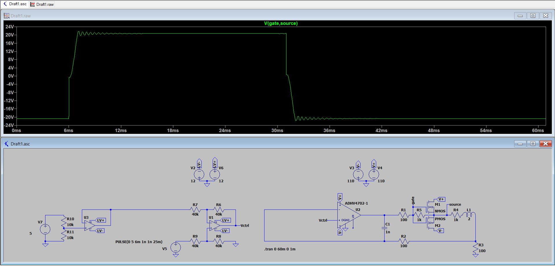
all in all, I relieved a lot of good feedback regarding the design and since there were no major issues, I decided to stick with the class B output amplifier. However finding high voltage BJTs was very difficult and only 1 or 2 parts came up which were any good for the job! I tried using fets which at first seemed like a great idea since I could find tons of them for high voltage applications with suitable SOA, etc. but after running the simulations, I noticed the resistor I used to eliminate crossover distortion (R5) , was actually making the FETs useless since it was too low of a value  :-DD I bumped it to 1k since the 25mA target goal is right on the limit of what the op amp can do, which is why I need the boosting stage to begin with. now the fets do the job but the gate-source voltage is outside the rating of the fets (picture attached) :palm: In hindsight that's obvious since 10v (max Vgs) at 25mA is about 400\$\Omega\$
780846-0

now to the main questions:
1)the gates and sources are shared, so I can't simply use a zener since it clamps to 0.3V on one half of the signal which is no good! maybe 2 zeners back to back can do the trick? I'm not sure if they are fast enough though (<1mS reaction time)

2)Is there another way to reduce the crossover distortion without having R5? (I'm not sure how I can bias a FET to make a class AB amplifier  :palm:)

3)Maybe other output element types would be more suitable? perhaps I should look into high voltage IGBTs?

4)Any other suggestions about a better / simpler approach (not about using lower voltages or a H bridge with single supply approach for driving the inductor , just about solutions to the amplifier problem please! I'd like to keep this as close to the attached schematic as possible since I have designed it and it's important for my final submission since I have to explain how and why things work :P)
« Last Edit: July 09, 2019, 06:49:20 pm by OM222O »
 

Online strawberry

  • Super Contributor
  • ***
  • Posts: 1161
  • Country: lv
Re: problems with a class B amplifier (high voltage)
« Reply #1 on: July 09, 2019, 08:17:28 pm »
BJT MOSFET sziklay compound and biasing will be as regular BJT Vbe=0.65V
 

Offline OM222OTopic starter

  • Frequent Contributor
  • **
  • Posts: 768
  • Country: gb
Re: problems with a class B amplifier (high voltage)
« Reply #2 on: July 10, 2019, 04:32:50 am »
can you please provide a schematic or more details? as I mentioned before, it's almost impossible to find a high voltage BJT, otherwise, I would have used them for the output stage to begin with (although I was looking for ones with enough DC SOA and TO-220package for heat sinking, so maybe they're not that rare!). this would also help with the crossover distortion and allow me to remove R5, but this doesn't fix the Vgs issue (in fact it makes it worse since op amp will shoot to the positive or negative rail when source is at almost 0 and Vgs becomes 100 volts).
 

Offline Zero999

  • Super Contributor
  • ***
  • Posts: 19519
  • Country: gb
  • 0999
Re: problems with a class B amplifier (high voltage)
« Reply #3 on: July 10, 2019, 10:19:07 am »
Why create another thread? It's less confusing if you keep it all in the same thread.

The ADHV4702-1 can almost do it. Add a couple of pass BJTs, which only need to pass 5mA or so.
 

Offline MagicSmoker

  • Super Contributor
  • ***
  • Posts: 1408
  • Country: us
Re: problems with a class B amplifier (high voltage)
« Reply #4 on: July 10, 2019, 10:58:38 am »
...
However finding high voltage BJTs was very difficult and only 1 or 2 parts came up which were any good for the job...

From what I recall of your other thread - which was a real dog's breakfast, to use the old British colloquialism - you need to drive a highly inductive actuator with up to +/-100V at 25mA, right? And you couldn't find appropriate complementary BJTs with the necessary >200V or so Vceo rating to fit the bill?

This defies belief because there should be hundreds of pairs suitable for the job: matched NPN/PNP pairs with moderate voltage and current rating are commonly used in audio amplifier driver and output stages, after all.

Here's the start of a Farnell UK search for single BJTs that are in stock; you can further whittle down the list by Vceo rating, package, Ic rating, etc.:

https://uk.farnell.com/w/c/semiconductors-discretes/transistors/bipolar-transistors/single-bipolar-junction-transistors-bjt?range=inc-in-stock

I suggest searching for PNP first then looking at the datasheet to see if there is a recommended complementary NPN part. Or you can simply infer the likelihood of a pair being complementary from their specs, as happens to be the case for the first two results in the above search (2SA1943 and 2SC5200; NB - 2SA parts are always PNP while 2SC parts are always NPN).


Online Marco

  • Super Contributor
  • ***
  • Posts: 6720
  • Country: nl
Re: problems with a class B amplifier (high voltage)
« Reply #5 on: July 10, 2019, 03:27:51 pm »
I'm not sure how I can bias a FET to make a class AB amplifier

Usually you just dial in the bias current with a potentiometer (to set the difference between the gate voltages).

Any way, how about this (opamp chosen at semi-random, the output transistors chosen by a 30 second parametric search). It's a variation on a high voltage amplifier described by Jim Williams.
 

Offline mikerj

  • Super Contributor
  • ***
  • Posts: 3240
  • Country: gb
Re: problems with a class B amplifier (high voltage)
« Reply #6 on: July 10, 2019, 04:48:50 pm »
The resistor values for the feedback divider need to be increased by an order of magnitude or two, the current ones will be dissipating up to 9 watts!
 

Offline OM222OTopic starter

  • Frequent Contributor
  • **
  • Posts: 768
  • Country: gb
Re: problems with a class B amplifier (high voltage)
« Reply #7 on: July 11, 2019, 07:01:39 am »
Why create another thread? It's less confusing if you keep it all in the same thread.

The ADHV4702-1 can almost do it. Add a couple of pass BJTs, which only need to pass 5mA or so.
(Attachment Link)

yes, but there are two problems with that:
1) the ADHV will be burning when dissipating about 2 watts or so (op amps are really not meant for driving loads!)
2) it's next to impossible to find suitable BJTs for the job

This defies belief because there should be hundreds of pairs suitable for the job: matched NPN/PNP pairs with moderate voltage and current rating are commonly used in audio amplifier driver and output stages, after all.

looking at farnell, this is the only part with proper DC SOA for the application:
https://uk.farnell.com/on-semiconductor/mje15035g/transistor-bipol-pnp-350v/dp/2535628

mouser is even worse with these results:
https://www.mouser.co.uk/Semiconductors/Discrete-Semiconductors/Transistors/Bipolar-Transistors-BJT/_/N-ax1sh?P=1z0y4ciZ1z0z63xZ1z0y4cnZ1yzub45Z1yzxobgZ1yyx4anZ1yzxod6Z1yyzr49Z1yyzroxZ1yyx4q4Z1yyx4q8Z1yyzrqt

All are TO-92  :palm: obviously no good for power applications (although 3 watts is not really power application, but it's definitely way too much for that package)

PNPs are the pain in the ass right now as they either lack collector base voltage (which is useless with a high collector emitter voltage ... I'm not even sure why those parts exist because base emitter voltage is usually less than 1v!) or the proper DC SOA.

NPNs are not as big of an issue.
https://www.mouser.co.uk/Semiconductors/Discrete-Semiconductors/Transistors/Bipolar-Transistors-BJT/_/N-ax1sh?P=1z0y4ciZ1z0z63xZ1z0y4diZ1y95l6hZ1z0y1zn&Rl=ax1shZer4gZ1yyzt9cZ1yyx4ozSGTax1shZer4hZ1z0w7eqZ1yyx4p3SGT&Ns=Pricing|1

Usually you just dial in the bias current with a potentiometer (to set the difference between the gate voltages).
Any way, how about this (opamp chosen at semi-random, the output transistors chosen by a 30 second parametric search). It's a variation on a high voltage amplifier described by Jim Williams.

your schematic uses a low voltage op amp + a voltage boost stage. that would be pointless with a high voltage op amp like the ADHV which I plan on using.
Also the transistors lack DC SOA once again, only about 10mA at 100v as opposed to 25  :-//

The resistor values for the feedback divider need to be increased by an order of magnitude or two, the current ones will be dissipating up to 9 watts!
I'm not sure which circuit you are talking about, perhaps the one posted by marco, because I've checked the power in my designs and non of the resistors (even at the transient peak, do more than about 50mW)

I will do some low voltage prototypes with mosfets to know how the biasing works. I'm not sure if I should use two normal diodes like the BJT biasing or two 5v zeners since the max Vgsthreshold for fets is about 4-5 volts. please provide a schematic on how to properly bias the fets rather than words if possible. thanks.
 

Offline magic

  • Super Contributor
  • ***
  • Posts: 6779
  • Country: pl
Re: problems with a class B amplifier (high voltage)
« Reply #8 on: July 11, 2019, 07:47:31 am »
You should be careful with MJE15034/MJE15035, their SOA is barely enough and appears to be specified at Tc=25°C. It seems like with BJTs you are limited to audio output transistors such as aforementioned 2SA1943/2SC5200. More choice would exist in a single rail design >:D

Before biasing anything, hack together a prototype and check if you really need it. If you do, you will also need another HV transistor for current source, unless you go for something unconventional like an isolated DC-DC converter or floating batteries.

I would discourage anything involving complementary common source FETs, like a BJT+FET Sziklai, on the grounds of crossconduction risk.
 

Offline mikerj

  • Super Contributor
  • ***
  • Posts: 3240
  • Country: gb
Re: problems with a class B amplifier (high voltage)
« Reply #9 on: July 11, 2019, 07:48:55 am »

The resistor values for the feedback divider need to be increased by an order of magnitude or two, the current ones will be dissipating up to 9 watts!
I'm not sure which circuit you are talking about, perhaps the one posted by marco, because I've checked the power in my designs and non of the resistors (even at the transient peak, do more than about 50mW)

Yes, Marco's circuit.
 

Online Marco

  • Super Contributor
  • ***
  • Posts: 6720
  • Country: nl
Re: problems with a class B amplifier (high voltage)
« Reply #10 on: July 11, 2019, 08:18:24 am »
It's not a divider, the 1.5k was what the other thread said the coil resistance is.
 

Offline OM222OTopic starter

  • Frequent Contributor
  • **
  • Posts: 768
  • Country: gb
Re: problems with a class B amplifier (high voltage)
« Reply #11 on: July 11, 2019, 09:11:59 am »
You should be careful with MJE15034/MJE15035, their SOA is barely enough and appears to be specified at Tc=25°C. It seems like with BJTs you are limited to audio output transistors such as aforementioned 2SA1943/2SC5200. More choice would exist in a single rail design >:D

Before biasing anything, hack together a prototype and check if you really need it. If you do, you will also need another HV transistor for current source, unless you go for something unconventional like an isolated DC-DC converter or floating batteries.

I would discourage anything involving complementary common source FETs, like a BJT+FET Sziklai, on the grounds of crossconduction risk.

That is exactly my point! There are less than a total of 5 parts I found that barely fit the apllication! That's why I'm consideeing fets now. For the supply I will be using batteries (A few 8s lipo packs) so no issues there!
Can you please explain the issue with common source arrangement? I could mix and match but I'm not sure if that's a good idea. I.e: use a P channel fet and a NPN BJT. That makes biasing a bit weird too. So I'm still open to suggestions.

Edit: the issue with the recommended parts is there is almost no headroom whatsoever! Vceo and Vcbo are 230V and the application needs 220V! Maybe lowering the input voltages can add some safety margin without slowing the response too much, but I'd like to have some margin. In my own search I started at 300volts to have a decent headroom.
« Last Edit: July 11, 2019, 09:20:27 am by OM222O »
 

Offline magic

  • Super Contributor
  • ***
  • Posts: 6779
  • Country: pl
Re: problems with a class B amplifier (high voltage)
« Reply #12 on: July 11, 2019, 10:09:14 am »
Can you please explain the issue with common source arrangement?
Look up what "common source" means and what a "Sziklai pair" is. Then don't use it :D
 

Offline MagicSmoker

  • Super Contributor
  • ***
  • Posts: 1408
  • Country: us
Re: problems with a class B amplifier (high voltage)
« Reply #13 on: July 11, 2019, 10:21:38 am »
Edit: the issue with the recommended parts is there is almost no headroom whatsoever! Vceo and Vcbo are 230V and the application needs 220V! Maybe lowering the input voltages can add some safety margin without slowing the response too much, but I'd like to have some margin. In my own search I started at 300volts to have a decent headroom.

MJx340/MJx350 are a commonly specified complementary pair for audio applications that have a 300V Vceo/Vcbo and a DC SOA of 50mA at 100V Vce and 125C Tj. NB - "x" specifies the package, and is E for TO-220, D for Dpak, etc. Dirt cheap, too.


Offline duak

  • Super Contributor
  • ***
  • Posts: 1041
  • Country: ca
Re: problems with a class B amplifier (high voltage)
« Reply #14 on: July 11, 2019, 05:17:46 pm »
Inductive loads can be difficult to drive and can exceed the SOA limits of the output devices unless the devices are saturated.  Work out the power dissipation in the output devices for various output voltages.  For a square wave, purely resistive loads have maximum dissipation at half voltage output.

If you go to BJT you'll have to provide clamping diodes from the output to the supply busses.

Back to back zener diodes are fine for protecting the gates of MOSFETs and IGBTs.  The zener or avalanche effect is quite fast - we're talking tens of ns if not faster.  What is slow is the diode shutting off in the forward direction ie., when it is operating as a normal diode.  It shouldn't be a problem here as the circuit is not operating at MHz rates.

I'm not sure that crossover distortion is a particularly big deal when the time constant of the load is L/R = 2H/ 1K0 = 2 ms.  There will be a bit of a deadband in the transfer function, but the overall negative feedback should bury it - at least at low frequencies.  However, if you're thinking of operating this at 10 KHz, and are expecting high accuracy, then it will be a problem.
 

Offline SiliconWizard

  • Super Contributor
  • ***
  • Posts: 14466
  • Country: fr
Re: problems with a class B amplifier (high voltage)
« Reply #15 on: July 11, 2019, 05:46:23 pm »
Hopefully the OP is not designing an electromagnetic brainwashing machine though.
 

Online Marco

  • Super Contributor
  • ***
  • Posts: 6720
  • Country: nl
Re: problems with a class B amplifier (high voltage)
« Reply #16 on: July 11, 2019, 06:43:51 pm »
please provide a schematic on how to properly bias the fets rather than words if possible. thanks.

You can probably do it simpler, but this should work. You can use your wallet killer opamp to drive the midpoint too.
 

Offline OM222OTopic starter

  • Frequent Contributor
  • **
  • Posts: 768
  • Country: gb
Re: problems with a class B amplifier (high voltage)
« Reply #17 on: July 12, 2019, 09:11:42 am »
Edit: the issue with the recommended parts is there is almost no headroom whatsoever! Vceo and Vcbo are 230V and the application needs 220V! Maybe lowering the input voltages can add some safety margin without slowing the response too much, but I'd like to have some margin. In my own search I started at 300volts to have a decent headroom.

MJx340/MJx350 are a commonly specified complementary pair for audio applications that have a 300V Vceo/Vcbo and a DC SOA of 50mA at 100V Vce and 125C Tj. NB - "x" specifies the package, and is E for TO-220, D for Dpak, etc. Dirt cheap, too.

Those parts are exactly what I was looking for, not sure why they don't show up in parametric search and I haven't done anything with audio designs before, so I didn't knew they existed!

Inductive loads can be difficult to drive and can exceed the SOA limits of the output devices unless the devices are saturated.  Work out the power dissipation in the output devices for various output voltages.  For a square wave, purely resistive loads have maximum dissipation at half voltage output.

If you go to BJT you'll have to provide clamping diodes from the output to the supply busses.

Back to back zener diodes are fine for protecting the gates of MOSFETs and IGBTs.  The zener or avalanche effect is quite fast - we're talking tens of ns if not faster.  What is slow is the diode shutting off in the forward direction ie., when it is operating as a normal diode.  It shouldn't be a problem here as the circuit is not operating at MHz rates.

I'm not sure that crossover distortion is a particularly big deal when the time constant of the load is L/R = 2H/ 1K0 = 2 ms.  There will be a bit of a deadband in the transfer function, but the overall negative feedback should bury it - at least at low frequencies.  However, if you're thinking of operating this at 10 KHz, and are expecting high accuracy, then it will be a problem.


I'm going with the MJE3x0 pair for the time being. I will include some 110V zener diodes from the output to each rail, but I'm not sure if I should also add a resistor in series with it and if not, what should the power rating be on the diodes?
maybe a MOV is better in these situations?

the actuator certainly won't be moving back and forth at 10KHz! the 1 to 2ms is just a requirement for the PID control loop to be stable, otherwise it will be reacting to old data and losing stability when the actuator actually moves.

I also realized that my resistor values for the base resistor and the base emitter resistors were quite low and the op amp was still doing the majority of the work, so I increased them. here is the schematic as it stands:
783081-0

also here is the power dissipated by each component (blue is the op amp, red is the PNP transistor and green is the NPN transistor):
783075-1
 

Offline MagicSmoker

  • Super Contributor
  • ***
  • Posts: 1408
  • Country: us
Re: problems with a class B amplifier (high voltage)
« Reply #18 on: July 12, 2019, 10:48:42 am »
MJx340/MJx350 are a commonly specified complementary pair for audio applications that have a 300V Vceo/Vcbo and a DC SOA of 50mA at 100V Vce and 125C Tj. NB - "x" specifies the package, and is E for TO-220, D for Dpak, etc. Dirt cheap, too.

Those parts are exactly what I was looking for, not sure why they don't show up in parametric search and I haven't done anything with audio designs before, so I didn't knew they existed!

FWIW, my specific search methodology to find a matched BJT pair is to first filter on PNP parts that are in stock because there are far fewer PNP parts, then select the range of Vceo, then the range of Ic, and, optionally the package(s). This usually results in a far more manageable list of candidates that I sort on ascending price to then start checking the datasheets for the recommended matched NPN device and application, though generally speaking, if a PNP device has a matching NPN device it is almost certainly going to be optimized for linear/amplifier applications rather than switching.
 

Offline duak

  • Super Contributor
  • ***
  • Posts: 1041
  • Country: ca
Re: problems with a class B amplifier (high voltage)
« Reply #19 on: July 12, 2019, 06:26:46 pm »
OM2220, the power dissipation graphs are quite interesting.  I can see the slight ringing in the load current expanded in the transistor power dissipation curves.  I think this circuit is underdamped.  I would increase the value of R2 to at least 1K0 and adjust C1 until I get a clean pulse response.  BTW, I think a value of 100R for R2 is too low and loading down the opamp output more than it needs to be.

Please show us want you want to do with the zener diodes.  MOVs are probably not the best choice for repetitive pulse voltage limiting.

Please try different output currents to confirm where the maximum power is dissipated.

I have no idea of what the payload of the actuator is.  It could be an optical element on an air bearing with an interferometric position sensor that would indeed be sensitive to high frequencies.
 

Offline OM222OTopic starter

  • Frequent Contributor
  • **
  • Posts: 768
  • Country: gb
Re: problems with a class B amplifier (high voltage)
« Reply #20 on: July 14, 2019, 07:44:16 am »
Here is what I meant by adding zeners (I won't use that exact part, just something with 110 to 120V breakdown voltage):
784653-0

again, I'm not sure if I need R12 and R13 and if I should just remove them?
as for the damping, I have asked and have been told that it's not an issue and to be honest I'm not sure how I can get the system to be "critically damped". Adding a capacitor across the actuator seems like the easiest option to add more damping but feel free to let me know how I can calculate the capacitor value to get correct damping.

here is also a DC sweep to analyze maximum powers (colors are the same as before):
784647-1

op amp has a maximum of 650mW and transistors have a max of about 4.2w which is manageable with some heat sinks.
The actuators are used in "force driven joints" based on data from pressure sensors.
 

Offline magic

  • Super Contributor
  • ***
  • Posts: 6779
  • Country: pl
Re: problems with a class B amplifier (high voltage)
« Reply #21 on: July 14, 2019, 12:35:06 pm »
But why? :scared:

Just make it a diode from output to V+ and from output to V- such that any transient is fed back into supply capacitors. Make sure they are big enough to absorb the energy.

As for ringing, experiment with C1 and R2 and probe opamp output and inverting input to see what's going on.
 

Offline OM222OTopic starter

  • Frequent Contributor
  • **
  • Posts: 768
  • Country: gb
Re: problems with a class B amplifier (high voltage)
« Reply #22 on: July 14, 2019, 02:01:19 pm »
But why? :scared:

Just make it a diode from output to V+ and from output to V- such that any transient is fed back into supply capacitors. Make sure they are big enough to absorb the energy.

As for ringing, experiment with C1 and R2 and probe opamp output and inverting input to see what's going on.

The output is the "emitter" net :-DD resistor is to just save the diode from high currents  :-// I'm not sure if this slows down the zener or not, but the connections are correct.
 

Offline duak

  • Super Contributor
  • ***
  • Posts: 1041
  • Country: ca
Re: problems with a class B amplifier (high voltage)
« Reply #23 on: July 16, 2019, 08:08:17 pm »
OM2220-
Because the load is an inductor it will not suddenly increase current unless its core saturates.  What it will do is generate a voltage that will try to maintain the current flowing through it.  If the driver is trying to increase current, the voltage will rise up to whatever is needed to oppose the change but limited to the supply voltage.  If there's already a high current and the driver is then commanded to deliver a lower or negative current, the opamp output and then the emitter voltage will snap down to whatever the inductor can generate to try to maintain the previous current.  In the limit, the emitter voltage will be slightly more negative than the negative supply. The load current will forward bias Q1's base-emitter junction and then Q2's base-collector junction.  Since Q1 has base current it will turn on and take collector current with a very high collector-emitter voltage leading to high dissipation, perhaps close to the SOA limits.  The opamp output will go to its negative limit and not accept too much current because of R1.   Zener D1 will conduct a current limited by R13.  This may be OK but most designs avoid it by putting clamp diodes between the emiiter net and the supply rails.  If you want to use zener diodes for clamps it's probably better to connect them back-to-back across the coil.

When you mention critically damped, do you mean the driver circuit or the whole electromechanical system?  The decaying sine wave tells me the driver is underdamped but not to the point of instability.  This can be dealt with by adjusting C1 and R1.  When you add the interaction of the coil with the actuator and payload the driver's damping won't change but the system damping will be determined by other characteristics. 


Share me

Digg  Facebook  SlashDot  Delicious  Technorati  Twitter  Google  Yahoo
Smf