Author Topic: Transistors - die pictures  (Read 190655 times)

0 Members and 2 Guests are viewing this topic.

Online NoopyTopic starter

  • Super Contributor
  • ***
  • Posts: 1734
  • Country: de
    • Richis-Lab
Re: Transistors - die pictures
« Reply #325 on: February 20, 2021, 05:45:33 am »
There are also MPSA transistors built by Philips. The one who gave me these transistors stated it is a Philips...  :-//

I know others make MPS and MPSA prefix transistors.  I just thought that prefix originated with Motorola and others are second sources.

You are right, Philips was definitely not the first one selling the MPSA56 but certainly this MPSA56 is a "Philips-MPSA".  :-+
« Last Edit: February 20, 2021, 05:47:04 am by Noopy »
 

Online NoopyTopic starter

  • Super Contributor
  • ***
  • Posts: 1734
  • Country: de
    • Richis-Lab
Re: Transistors - die pictures
« Reply #326 on: February 21, 2021, 08:53:01 pm »


Valvo ASZ16, a PNP-Ge-Powertransistor (32V, 10A, 250kHz).
The TO-3 package is interesting: The base plate is quite big. The datasheet states 3,4mm. But the cap is quite low (3,6mm).


Valvo not only mounted a dehumidifying element in the package, they also potted the free room with a silicone gel like material.


Meanwhile we know the stackup of a Ge-Powertransistors.


There are isolating plates on the contact pins. Probably that makes fabrication easier.


 :-+


https://www.richis-lab.de/Bipolar40.htm

 :-/O
 
The following users thanked this post: SilverSolder, RoGeorge

Online NoopyTopic starter

  • Super Contributor
  • ***
  • Posts: 1734
  • Country: de
    • Richis-Lab
Re: Transistors - die pictures
« Reply #327 on: February 25, 2021, 11:23:39 am »


Siemens BC239C


Nothing special...


https://www.richis-lab.de/Bipolar41.htm

 :-/O
 
The following users thanked this post: exe

Online NoopyTopic starter

  • Super Contributor
  • ***
  • Posts: 1734
  • Country: de
    • Richis-Lab
Re: Transistors - die pictures
« Reply #328 on: March 01, 2021, 07:08:47 pm »


The BUX66 is a pnp power transistor capable of isolating up to 350V and conducting up to 2A, 5Apeak.
They did quite some binning:
BUX66 150V
BUX66A 250V
BUX66B 300V
BUX66C 350V
This BUX66 built by Motorola seems to be quite new: 2005.


There is some silicone like potting on the die but the amount of potting is quite different in these two transistors.


Some damage due to the depotting...  :'(


The die is 3,6mm x 3,0mm.


It´s a MESA transistor with a nice trench at the edges of the die.


The structure is interesting. The left brown area is the p-doped emitter. The following green are is the n-doped base. In the next pictures we will see that this is the base-emitter-junction.
Before the base contact there is a small brown p-doped layer certainly above the base area. Why that? Looks like a pinch resistor to increase the base resistance. But why would they increase the base resistance? Perhaps the resistance is equalising the electric stress on the transistor area?  :-//


That´s the base emitter junction!  8)
(13,5V / 20mA)


Looks like a very uniform transistor structure.


0,8A  8)


https://www.richis-lab.de/Bipolar42.htm

 :-/O
 
The following users thanked this post: SeanB, exe, SilverSolder, RoGeorge

Online NoopyTopic starter

  • Super Contributor
  • ***
  • Posts: 1734
  • Country: de
    • Richis-Lab
Re: Transistors - die pictures
« Reply #329 on: March 02, 2021, 04:52:39 am »


Today I´m pretty sure that´s a conterfeit part:
- 2005 Motorola was already ON Semiconductor.
- In the "Motorola Semiconductor Master Selection Guide 1994" there is already no TO-66 package left.
- Up to now I found such a white potting just in the conterfeit BUX22 (https://www.richis-lab.de/Bipolar09.htm) and in the Inchange 3DD15D (https://www.richis-lab.de/Bipolar05.htm)
- The strange additional "ring" between base and emitter was also only found in the conterfeit BUX22 and in the Inchange 3DD15D.

 >:D

Offline exe

  • Supporter
  • ****
  • Posts: 2562
  • Country: nl
  • self-educated hobbyist
Re: Transistors - die pictures
« Reply #330 on: March 02, 2021, 11:26:55 am »
I was about to say how well it's made :).

Perhaps there are many manufacturer in Asia that I've never heard of and who are producing parts like that (assuming it's from China). I found many parts that are absolete but yet cloned/produced/available. Like some jfets for mic pre-amps.
 

Offline SilverSolder

  • Super Contributor
  • ***
  • Posts: 6126
  • Country: 00
Re: Transistors - die pictures
« Reply #331 on: March 02, 2021, 03:38:05 pm »


Today I´m pretty sure that´s a conterfeit part:
- 2005 Motorola was already ON Semiconductor.
- In the "Motorola Semiconductor Master Selection Guide 1994" there is already no TO-66 package left.
- Up to now I found such a white potting just in the conterfeit BUX22 (https://www.richis-lab.de/Bipolar09.htm) and in the Inchange 3DD15D (https://www.richis-lab.de/Bipolar05.htm)
- The strange additional "ring" between base and emitter was also only found in the conterfeit BUX22 and in the Inchange 3DD15D.

 >:D

Maybe the clean and uniform transistor structure that you found in the original post is a sign that it has been manufactured with a more modern process than the original?

Perhaps we ought to set up a "Counterfeit Test Program" to reveal which counterfeits are, in fact, quite good,  and which are not good?   :D
 

Online NoopyTopic starter

  • Super Contributor
  • ***
  • Posts: 1734
  • Country: de
    • Richis-Lab
Re: Transistors - die pictures
« Reply #332 on: March 02, 2021, 05:12:17 pm »
This BUX66 definitely looks like a big good transistor.  :-+ Nevertheless it is a conterfeit part... But maybe good to use.  :-//

Testing these transistors would be very interesting but would need a lot more time and equipment.  :-\
 
The following users thanked this post: SilverSolder

Online NoopyTopic starter

  • Super Contributor
  • ***
  • Posts: 1734
  • Country: de
    • Richis-Lab
Re: Transistors - die pictures
« Reply #333 on: March 03, 2021, 12:27:16 pm »
Siemens BC239C


Today: Philips BC239C


Interesting: The Philips BC239C looks exactly the same as the Siemens BC239C, same structures, same size!
I had to look twice because in the first place I wasn´t perfectly sure if I really had taken the Philips die and not the Siemens die by accident. But now I´m sure the Philips die is the same as the Siemens die.


https://www.richis-lab.de/Bipolar41.htm

 :-/O
 
The following users thanked this post: exe

Online NoopyTopic starter

  • Super Contributor
  • ***
  • Posts: 1734
  • Country: de
    • Richis-Lab
Re: Transistors - die pictures
« Reply #334 on: March 06, 2021, 08:47:38 pm »


Motorola 2N2152, a Ge-PNP-Powertransistor: 30V, 30A, 2kHz. There are two more bins giving you 45V and 60V.
The 2N2152 is especially interesting compared to the 15A-line around the 2N2081 (https://www.richis-lab.de/Bipolar28.htm).


The huge TO-36-packages makes 170W (@25°C) possible.  8)


A metal ring is carrying a n-doped germanium disk which is the base. On both sides of the disk there is an alloyed area giving you p-dopant for emitter and collector.


But wait! While in the 2N2081 there is a second base contact in the middle of the disk here it is missing. That explains the higher collector current (30A vs. 15A). The disk diameter is exactly the  same in the 2N2152 and in the 2N2081 but without the central base contact you have a much bigger emitter area. The drawback is a lower cutoff frequency (2kHz vs. 5kHz) since the base impedance is higher.


Quite a big emitter contact!  :-+


https://www.richis-lab.de/Bipolar43.htm

 :-/O
 
The following users thanked this post: edavid, SilverSolder, RoGeorge

Online NoopyTopic starter

  • Super Contributor
  • ***
  • Posts: 1734
  • Country: de
    • Richis-Lab
Re: Transistors - die pictures
« Reply #335 on: March 09, 2021, 09:06:21 am »
Some more transistor dust!  ;D


BC547C, pretty the same as the BC550 (https://www.richis-lab.de/Bipolar39.htm) but the maximum noise figure is a bit higher: 10dB vs. 4dB
The base-emitter-junction is a little bit more robust: -6V vs. -5V. Probably the base doping of the BC550 is a bit higher. That gives you lower base resistance which gives you lower thermal noise but also reduces the base emitter breakdown voltage.


Hey, that´s exactly the same die as in the BC550 (https://www.richis-lab.de/Bipolar39.htm)! It seems like they just did some binning.
A die with 0,27mm edge length is really fun to handle.  >:D


https://www.richis-lab.de/Bipolar44.htm

 :-/O
 
The following users thanked this post: brabus, exe, SilverSolder

Online NoopyTopic starter

  • Super Contributor
  • ***
  • Posts: 1734
  • Country: de
    • Richis-Lab
Re: Transistors - die pictures
« Reply #336 on: March 11, 2021, 06:20:59 pm »


Today something new: Rohm DTC114, a digital transistor.


The die is 0,35mm x 0,35mm.


Well that´s quite clear.  :-+
Interesting point: The resistors have a different color. They probably used a special material to get the high resistance in this small area.


https://www.richis-lab.de/Bipolar45.htm

 :-/O
 
The following users thanked this post: edavid

Online T3sl4co1l

  • Super Contributor
  • ***
  • Posts: 21686
  • Country: us
  • Expert, Analog Electronics, PCB Layout, EMC
    • Seven Transistor Labs
Re: Transistors - die pictures
« Reply #337 on: March 11, 2021, 10:43:54 pm »
Y'know, I don't think I ever tested one of those for Vbc.  I suppose the resistors are on top of oxide, not diffused into the collector, so that wouldn't matter.  I wonder if amorphous or poly-Si, or metal or what?

Tim
Seven Transistor Labs, LLC
Electronic design, from concept to prototype.
Bringing a project to life?  Send me a message!
 

Online NoopyTopic starter

  • Super Contributor
  • ***
  • Posts: 1734
  • Country: de
    • Richis-Lab
Re: Transistors - die pictures
« Reply #338 on: March 12, 2021, 04:17:20 am »
I had the same opinion. Probably it´s some lower doped polysilicon. I assume the resistance of metal would be to low.

One would need to curve trace Vbc vs. Ibc to see the resistor... ...or not...  :-/O

Offline exe

  • Supporter
  • ****
  • Posts: 2562
  • Country: nl
  • self-educated hobbyist
Re: Transistors - die pictures
« Reply #339 on: March 13, 2021, 09:28:19 am »
The die is 0,35mm x 0,35mm.

Still can't wrap my head around how they cut and pack such tiny dies. Is it laser-cut yet or still cut by a saw? The BC547C has rough edges, I'd assume that one was cut by a saw.
 

Online NoopyTopic starter

  • Super Contributor
  • ***
  • Posts: 1734
  • Country: de
    • Richis-Lab
Re: Transistors - die pictures
« Reply #340 on: March 13, 2021, 10:38:44 am »
Well I don´t know...  :-//

Offline capt bullshot

  • Super Contributor
  • ***
  • Posts: 3033
  • Country: de
    • Mostly useless stuff, but nice to have: wunderkis.de
Re: Transistors - die pictures
« Reply #341 on: March 13, 2021, 12:45:58 pm »
Well I don´t know...  :-//

I vaguely remember, the wafer gets scribed along the lines between the dice, then attached to some elastic material and pulled apart to separate the dice.

Safety devices hinder evolution
 

Offline Miyuki

  • Frequent Contributor
  • **
  • Posts: 905
  • Country: cz
    • Me on youtube
Re: Transistors - die pictures
« Reply #342 on: March 15, 2021, 05:56:52 pm »
Well I don´t know...  :-//

I vaguely remember, the wafer gets scribed along the lines between the dice, then attached to some elastic material and pulled apart to separate the dice.
So like most brittle materials (glass, ceramic)
Makes sense
No mess and waste
 

Online NoopyTopic starter

  • Super Contributor
  • ***
  • Posts: 1734
  • Country: de
    • Richis-Lab
Re: Transistors - die pictures
« Reply #343 on: March 17, 2021, 10:21:12 pm »


Tesla KD605, a NPN-Powertransistor for linear operation like the KD501 (https://www.richis-lab.de/Bipolar02.htm).
Both the KD501 and the KD605 can isolate 40V but the KD501 can conduct 20A compared to 10A for the KD605. Also the maximum power dissipation is quite different: 150W vs. 70W. Surprisingly the dies in the packages look the same. Probably the more massive package of the KD501 gives you a lot more power. Perhaps there was also some binning.


The die is potted with some red silicone like material.
The die of the KD501 is soldered directly to the package. Here there is a round carrier.


Looks similar to the KD501.


Besides the MESA structure we see kind of a step at the uppermost layer. That could be the collector base junction but more likely it is an isolating silicon oxide layer.


Interesting, there are some very small steps in the base-emitter-junction.


 8)
-9V / 100mA


1A


https://www.richis-lab.de/Bipolar46.htm

 :-/O
 
The following users thanked this post: daqq

Offline daqq

  • Super Contributor
  • ***
  • Posts: 2302
  • Country: sk
    • My site
Re: Transistors - die pictures
« Reply #344 on: March 17, 2021, 10:37:09 pm »
Thanks for the great work!
Perhaps there was also some binning.
Yup, this was likely the case. Legend has it that Tesla did not gave great process yields or repeatability and they did a lot of binning for semiconductors.

An interesting analysis would be a silicon capacitor ( https://www.mouser.sk/Passive-Components/Capacitors/Silicon-RF-Capacitors-Thin-Film/_/N-5g95 ). Some seem to have far more advanced structures on them :)
Believe it or not, pointy haired people do exist!
+++Divide By Cucumber Error. Please Reinstall Universe And Reboot +++
 

Online NoopyTopic starter

  • Super Contributor
  • ***
  • Posts: 1734
  • Country: de
    • Richis-Lab
Re: Transistors - die pictures
« Reply #345 on: March 17, 2021, 10:47:55 pm »
Thanks for the great work!

Thanks!  8)


Perhaps there was also some binning.
Yup, this was likely the case. Legend has it that Tesla did not gave great process yields or repeatability and they did a lot of binning for semiconductors.

But I assume besides the binning the more massive package has also some effect.


An interesting analysis would be a silicon capacitor ( https://www.mouser.sk/Passive-Components/Capacitors/Silicon-RF-Capacitors-Thin-Film/_/N-5g95 ). Some seem to have far more advanced structures on them :)


Sounds interesting! I´ll put them on my list.  :-+


Offline SilverSolder

  • Super Contributor
  • ***
  • Posts: 6126
  • Country: 00
Re: Transistors - die pictures
« Reply #346 on: March 17, 2021, 10:48:45 pm »
[...]Tesla KD605[...]

So who's hiding inside that transistor, then?  :D


Online NoopyTopic starter

  • Super Contributor
  • ***
  • Posts: 1734
  • Country: de
    • Richis-Lab
Re: Transistors - die pictures
« Reply #347 on: March 17, 2021, 10:53:15 pm »
So who's hiding inside that transistor, then?  :D

 ;D

Online NoopyTopic starter

  • Super Contributor
  • ***
  • Posts: 1734
  • Country: de
    • Richis-Lab
Re: Transistors - die pictures
« Reply #348 on: March 20, 2021, 09:11:01 pm »


https://www.richis-lab.de/Bipolar46.htm

I have to correct myself: The die of the KD605 is a little smaller than the die of the KD601: 4,5mm vs. 5,5mm edge length. I have lost one mm.  ::) But that doesn´t explain the lower power rating completely...

Online NoopyTopic starter

  • Super Contributor
  • ***
  • Posts: 1734
  • Country: de
    • Richis-Lab
Re: Transistors - die pictures
« Reply #349 on: March 22, 2021, 08:26:27 am »


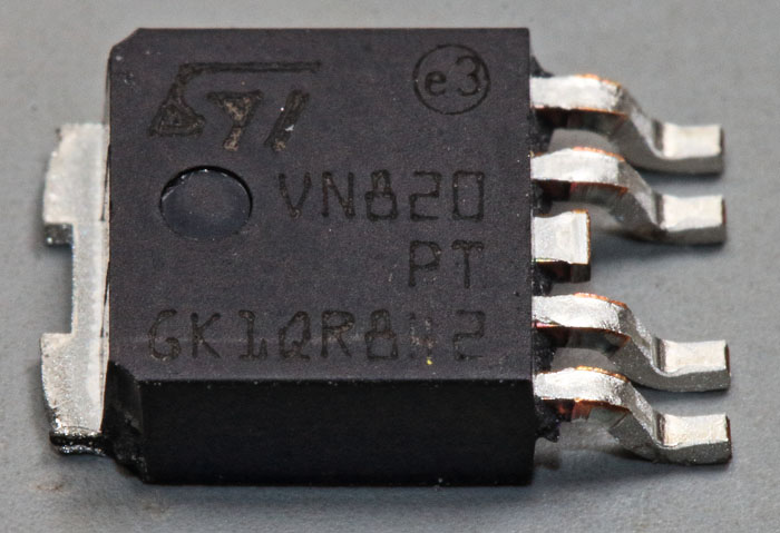
The STMicroelectronics VN820 is a Highside Smart-MOSFET of the third generation "M0-3".
The VN02H (https://www.richis-lab.de/FET02.htm) is of the first generation "M0-1".
The VN820 gives you 9A at 40m \$\Omega\$. Maximum isolation voltage is 55V (Clamping).


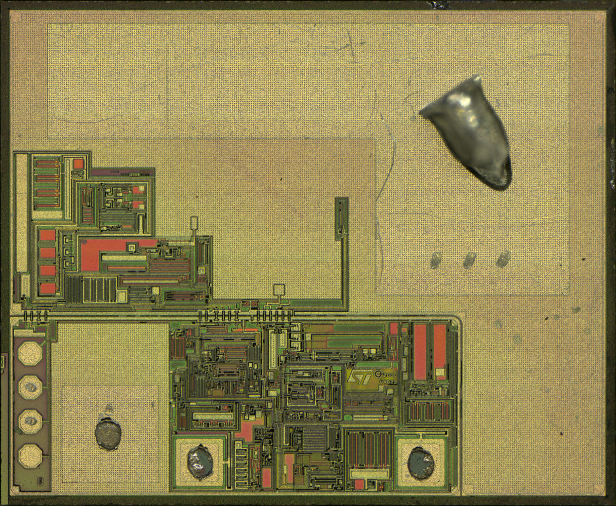
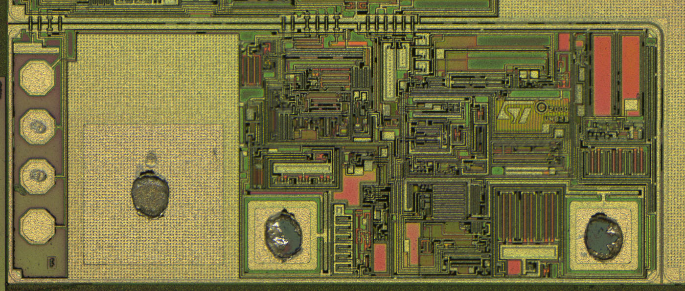
The die is 3,2mm x 2,6mm.


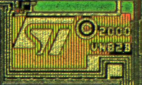
The design is named VN82B and was created in the year 2000.


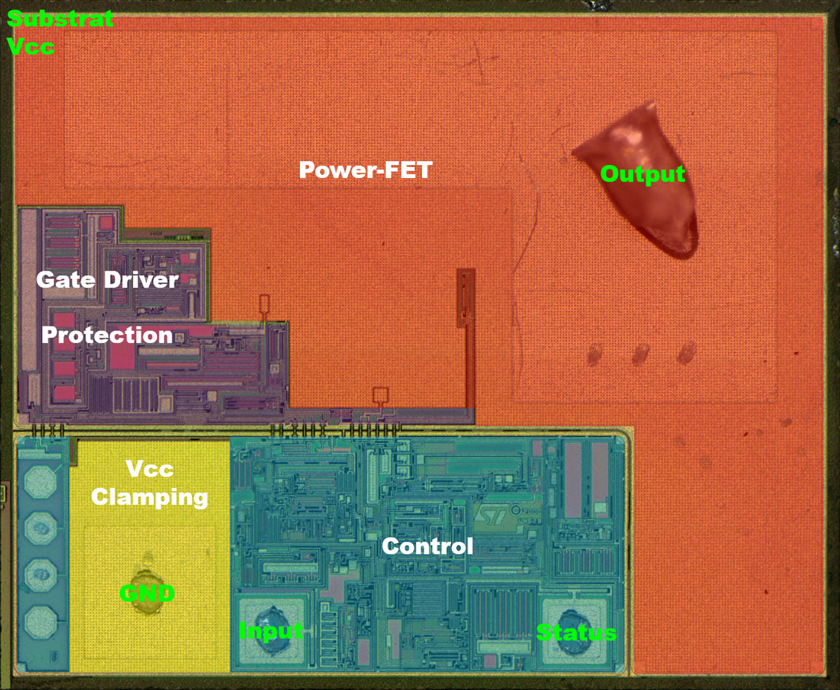
The die is divided in two pieces.
The power transistor (red) is integrated in the same frame as the driver circuit (purple). They share the source potential as reference.
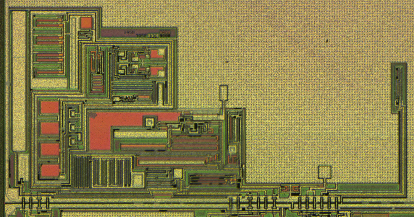
The second frame shares the GND potential as reference. In this frame there is the control circuit and the Vcc clamp which protects the devices against overvoltages on the supply line.
The main power transistor connects Vcc (substrate) to Output. The Vcc-Clamp connects Vcc (substrate) to GND.


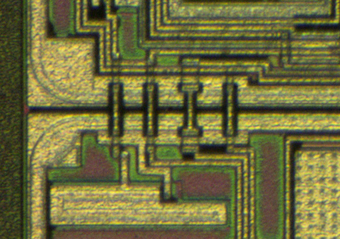
An interesting connection between the two areas.


In the driver area there are some capacitors some probably storing the energy to charge the gate of the output transistor.
It seems like there are also some protection circuits in this area to keep reaction time short.


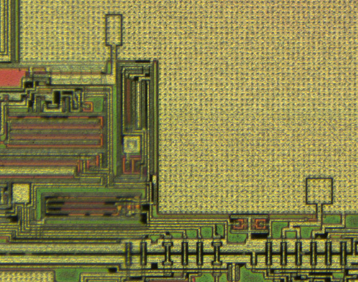
There are two small current sensing transistors. One transistor is connected to the driver circuits, one transistor is connected to the control circuit. The control circuit needs the current value for open load detection. The VN920 gives you a current sense output. Perhaps they use the same die.


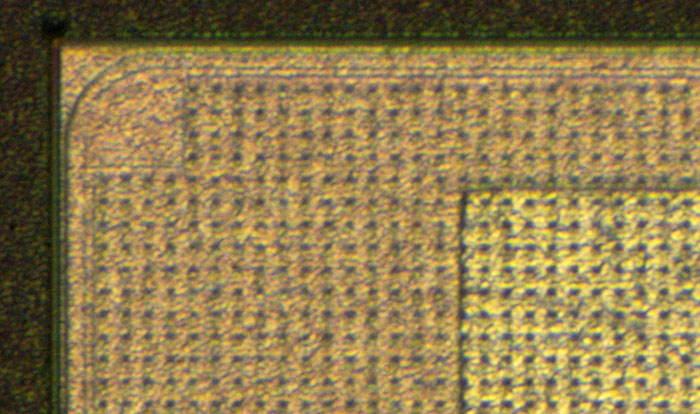
Well the power transistor is a big MOSFET.  ;D
In the corners there are free squares. That looks like electrical field steering but I don´t think that is what these structures are for.


The control circuit and the Vcc clamp.


Some more pictures here:

https://www.richis-lab.de/FET13.htm
 
The following users thanked this post: edavid, RoGeorge, capt bullshot, Jo


Share me

Digg  Facebook  SlashDot  Delicious  Technorati  Twitter  Google  Yahoo
Smf