Author Topic: Transistors - die pictures  (Read 190449 times)

0 Members and 3 Guests are viewing this topic.

Online T3sl4co1l

  • Super Contributor
  • ***
  • Posts: 21685
  • Country: us
  • Expert, Analog Electronics, PCB Layout, EMC
    • Seven Transistor Labs
Re: Transistors - die pictures
« Reply #400 on: May 27, 2021, 08:40:47 pm »
This is why most larger IGBT modules are gel filled. The gel absorbs the energy quite efficiently and doesn't create shrapnels.

Yeah, that helps -- the difference is whether enough energy was released to blast the cover off it (and I suppose, launch bits of goo).  Arc flash is serious business. :o

Basically the difference between a semiconductor fuse right at the device*, versus at the mains inlet (or any fuse type), is how much shrapnel is produced. ;D

*Not that you'd do this on a switching inverter, but upstream of minimal value bypass caps, perhaps.

Tim
Seven Transistor Labs, LLC
Electronic design, from concept to prototype.
Bringing a project to life?  Send me a message!
 

Offline capt bullshot

  • Super Contributor
  • ***
  • Posts: 3033
  • Country: de
    • Mostly useless stuff, but nice to have: wunderkis.de
Re: Transistors - die pictures
« Reply #401 on: May 27, 2021, 08:47:25 pm »
This is why most larger IGBT modules are gel filled. The gel absorbs the energy quite efficiently and doesn't create shrapnels.

Yeah, that helps -- the difference is whether enough energy was released to blast the cover off it (and I suppose, launch bits of goo).  Arc flash is serious business. :o

Basically the difference between a semiconductor fuse right at the device*, versus at the mains inlet (or any fuse type), is how much shrapnel is produced. ;D

*Not that you'd do this on a switching inverter, but upstream of minimal value bypass caps, perhaps.

Tim

None of these had semiconductor fuses installed, just the usual line fuses, and the usual DC link capacitors ...
I've seen the aftermath of bigger booms than these, but the covers weren't blasted off, and the goo stays in place. Plasma and / or arcs can escape and leave a lot of blackened stuff, but no flying parts around from these modules. I've seen other stuff (like AC input bridge rectifiers, electrolytic DC link capacitors) explode more violently.

Yes, this stuff gets blown intentionally as part of product safety testing.

« Last Edit: May 27, 2021, 08:49:09 pm by capt bullshot »
Safety devices hinder evolution
 

Offline David Hess

  • Super Contributor
  • ***
  • Posts: 16615
  • Country: us
  • DavidH
Re: Transistors - die pictures
« Reply #402 on: May 27, 2021, 11:47:53 pm »
Yeah, that helps -- the difference is whether enough energy was released to blast the cover off it (and I suppose, launch bits of goo).

For the record, the plastic bits from plastic encapsulation will puncture skin and stick in you.  A face shield would not be out of line when doing that sort of development work.
« Last Edit: May 27, 2021, 11:51:12 pm by David Hess »
 
The following users thanked this post: T3sl4co1l

Offline David Hess

  • Super Contributor
  • ***
  • Posts: 16615
  • Country: us
  • DavidH
Re: Transistors - die pictures
« Reply #403 on: May 27, 2021, 11:50:51 pm »
That´s a dead Motorola MJ802 (90V/30A/2MHz/200W).

I have a parts drawer full of good ones, and some of the complementary parts.
 

Online T3sl4co1l

  • Super Contributor
  • ***
  • Posts: 21685
  • Country: us
  • Expert, Analog Electronics, PCB Layout, EMC
    • Seven Transistor Labs
Re: Transistors - die pictures
« Reply #404 on: May 27, 2021, 11:54:04 pm »
None of these had semiconductor fuses installed, just the usual line fuses, and the usual DC link capacitors ...
I've seen the aftermath of bigger booms than these, but the covers weren't blasted off, and the goo stays in place. Plasma and / or arcs can escape and leave a lot of blackened stuff, but no flying parts around from these modules. I've seen other stuff (like AC input bridge rectifiers, electrolytic DC link capacitors) explode more violently.

Yes, this stuff gets blown intentionally as part of product safety testing.

Hmm, lucky!

Oh, also, that's one of those with the snap-on cover with some holes/slots in it, right?  They may vent well enough to avoid utter explosion.  That's no guarantee of course, just a matter of scale -- put enough power into anything, and all that.

Those are, usually smaller in size I think?  Maybe they're making bigger ones now, but I don't recall much beyond 1200V/250-300A as of about a decade ago.  The bigger ones usually have a rigid cover on top, which doesn't have any obvious venting paths as far as I can recall.  (The big ones we were using, were full bridge 1200V/600A I think.)

And the "next size up" bridge rectifier modules, are made the same way I think, not fully potted but probably using some goo or something, and a rigid shell?  Don't think I've seen any with the snap cover like those low profile IGBT modules anyway.

Tim
Seven Transistor Labs, LLC
Electronic design, from concept to prototype.
Bringing a project to life?  Send me a message!
 

Offline capt bullshot

  • Super Contributor
  • ***
  • Posts: 3033
  • Country: de
    • Mostly useless stuff, but nice to have: wunderkis.de
Re: Transistors - die pictures
« Reply #405 on: May 28, 2021, 05:45:36 am »
Yes, the large one had a snap-on cover. The other ones had covers with no holes. Anyway,  a cracked cover (but still in one piece) has been seen, normally the module stays in one piece. Larger ones aren't that flat profile anymore, but still gel filled construction and no hard potting.

Rectifiers and SCR modules I've seen are of different construction, they use disc SCR / diodes, pressure contacts, large conductors and hard enclosure material  These hard packaged ones break into pieces and crumbles, as they are buried deep within the complete unit while testing, there's not a big chance of shrapnel flying around. You'd still use adequate protection for your personal safety.
SCR and diodes in gel filled packages exist, usually that flat package. These have no large holes or covers to to vent, but don't explode. For smaller sizes, one can get flat profile modules with input rectifier, output bridge and chopper transistor in one package.

Older bridge rectifiers had hard packaging and potting, these exploded quite nicely ;)
« Last Edit: May 28, 2021, 05:49:06 am by capt bullshot »
Safety devices hinder evolution
 

Online NoopyTopic starter

  • Super Contributor
  • ***
  • Posts: 1734
  • Country: de
    • Richis-Lab
Re: Transistors - die pictures
« Reply #406 on: May 31, 2021, 06:45:09 pm »


Clevite 2N257, a germanium power transistor: 35V / 4A


Some drying agent.


Now that are a interesting contact electrodes. There had been one single element that was cut into base and emitter in two places.


The germanium plate is connected to a disk that is soldered to the base electrode.


Here we have the emitter contact on the germanium disk.


After removing the residues of the lid we can see the collector part of the transistor.


https://www.richis-lab.de/Bipolar58.htm

 :-/O
 
The following users thanked this post: SeanB, SilverSolder, capt bullshot

Online NoopyTopic starter

  • Super Contributor
  • ***
  • Posts: 1734
  • Country: de
    • Richis-Lab
Re: Transistors - die pictures
« Reply #407 on: June 06, 2021, 04:44:54 am »


STP3NB100FP, another Power-MOSFET (1000V, 3A, 5,3 \$\Omega\$).


The die is 3,9mm x 3,7mm.


The STP3NB100 doesn´t use the small square transistors we have seen in other power transistors. The datasheet calls it "strip layout".


The electrical field steering is mentioned in the datasheet too and looks quite interesting.
Most transistors use toroidal lines. Here we have squares with different size.  :-//


https://www.richis-lab.de/FET15.htm

 :-/O
 
The following users thanked this post: SilverSolder, RoGeorge, Miyuki

Offline SilverSolder

  • Super Contributor
  • ***
  • Posts: 6126
  • Country: 00
Re: Transistors - die pictures
« Reply #408 on: June 06, 2021, 01:54:39 pm »
[...]
Most transistors use toroidal lines. Here we have squares with different size.  :-//
[...]


Perhaps a French design?  French engineers often like to do things different...  (think Citroën)


Online NoopyTopic starter

  • Super Contributor
  • ***
  • Posts: 1734
  • Country: de
    • Richis-Lab
Re: Transistors - die pictures
« Reply #409 on: June 06, 2021, 03:38:26 pm »
[...]
Most transistors use toroidal lines. Here we have squares with different size.  :-//
[...]


Perhaps a French design?  French engineers often like to do things different...  (think Citroën)

Sound reasonable!  :)

Online NoopyTopic starter

  • Super Contributor
  • ***
  • Posts: 1734
  • Country: de
    • Richis-Lab
Re: Transistors - die pictures
« Reply #410 on: June 10, 2021, 12:40:40 pm »


SU111, a Darlington-Transistor built by Gleichrichterwerk Stahnsdorf.
400V, 10A/15A, 120W


Quite a high socket on which the die is placed.
A small bondwire for the base current and a thick bondwire for the emitter current.


The silicon is quite easy to remove.


The upper part of the die is the driver transistor part. The lower part of the die is the power transistor part.


It´s a MESA transistor. Etching the trench did quite some damage to the surface nearby.


Base-Emitter-junction...


Removing the metal layer gives us some more details.


In my view the setup looks like this.


Current that flows into the base of the driver transistor activates a current flow from its collector to its emitter.
The emitter current of the driver transistor is directed to the base of the power transistor and activates this transistor.
I assume the blue rectangle in the base of the driver transistor throttles the base current so that this base current doesn´t switch the power transistor directly. Not sure about that.  :-//


The resistor R1 is part of the base layer. To get the resistor R2 the base layer connects the T2 emitter metal layer through the emitter layer.
Switching the SU111 off the free charges in the driver transistor flow through R1 to the emitter of the power transistor. The free charges of the power transistor take the same way to the emitter.
The "hole" in the emitter layer of the power transistor has a second purpose. It gives you the emitter-collector-diode that you need in half bridge or H-bridge configurations.


https://www.richis-lab.de/Bipolar59.htm

 :-+

 
The following users thanked this post: SeanB, SilverSolder, RoGeorge

Offline SilverSolder

  • Super Contributor
  • ***
  • Posts: 6126
  • Country: 00
Re: Transistors - die pictures
« Reply #411 on: June 10, 2021, 02:02:04 pm »

Interesting, I didn't know that Darlingtons were implemented on a single chip like that...  makes sense, obviously.
 

Online NoopyTopic starter

  • Super Contributor
  • ***
  • Posts: 1734
  • Country: de
    • Richis-Lab
Re: Transistors - die pictures
« Reply #412 on: June 10, 2021, 02:13:40 pm »

Interesting, I didn't know that Darlingtons were implemented on a single chip like that...  makes sense, obviously.

I have opened a MJ3001. Looks different but quite similar.  ;D Coming soon...  :-/O

 
The following users thanked this post: SeanB, SilverSolder

Offline magic

  • Super Contributor
  • ***
  • Posts: 6779
  • Country: pl
Re: Transistors - die pictures
« Reply #413 on: June 10, 2021, 10:42:18 pm »
Interesting, I didn't know that Darlingtons were implemented on a single chip like that...  makes sense, obviously.
Old story, Sidney Darlington had a patent on that.

Quote
8. A signal translating device comprising a body of semi-conductive material having therein a first zone of one conductivity type, a pair of spaced zones of the opposite conductivity type contiguous with said first zone and a pair of zones of said one type each contiguous with a respective one of said first pair of zones, and remote from the other, means electrically connectin one of said first pair of zones to the one of said second pair of zones remote therefrom, and individual electrical connections to said first zone, the other of said first pair of zones and the other of said second pair of zones.
 
The following users thanked this post: SilverSolder, Miyuki

Online NoopyTopic starter

  • Super Contributor
  • ***
  • Posts: 1734
  • Country: de
    • Richis-Lab
Re: Transistors - die pictures
« Reply #414 on: June 11, 2021, 03:06:11 am »
Interesting, I didn't know that Darlingtons were implemented on a single chip like that...  makes sense, obviously.
Old story, Sidney Darlington had a patent on that.

Quote
8. A signal translating device comprising a body of semi-conductive material having therein a first zone of one conductivity type, a pair of spaced zones of the opposite conductivity type contiguous with said first zone and a pair of zones of said one type each contiguous with a respective one of said first pair of zones, and remote from the other, means electrically connectin one of said first pair of zones to the one of said second pair of zones remote therefrom, and individual electrical connections to said first zone, the other of said first pair of zones and the other of said second pair of zones.

But that sounds more like the (Motorola) MJ3001 (coming soon): Two transistors on one die separated except for the collector.
By contrast the SU111 share the base layer.
« Last Edit: June 11, 2021, 03:08:21 am by Noopy »
 

Offline magic

  • Super Contributor
  • ***
  • Posts: 6779
  • Country: pl
Re: Transistors - die pictures
« Reply #415 on: June 11, 2021, 08:50:05 am »
Good observation. I wonder if that base-to-base resistor could make this device exempt from Darlington's patent :-DD
Perhaps not, because it had other, more general claims.

BTW, US2663806 was granted in 1953 so it should have expired long, long ago and not be a concern in any remotely modern design.
« Last Edit: June 11, 2021, 08:57:08 am by magic »
 

Offline dzseki

  • Frequent Contributor
  • **
  • Posts: 509
  • Country: hu
Re: Transistors - die pictures
« Reply #416 on: June 11, 2021, 09:02:36 am »
Good observation. I wonder if that base-to-base resistor could make this device exempt from Darlington's patent :-DD
Perhaps not, because it had other, more general claims.

BTW, US2663806 was granted in 1953 so it should have expired long, long ago and not be a concern in any remotely modern design.

Not that eastern block companies gave much on western patents, eh? :)
HP 1720A scope with HP 1120A probe, EMG 12563 pulse generator, EMG 1257 function generator, EMG 1172B signal generator, MEV TR-1660C bench multimeter
 
The following users thanked this post: Miyuki

Online NoopyTopic starter

  • Super Contributor
  • ***
  • Posts: 1734
  • Country: de
    • Richis-Lab
Re: Transistors - die pictures
« Reply #417 on: June 12, 2021, 03:35:07 am »


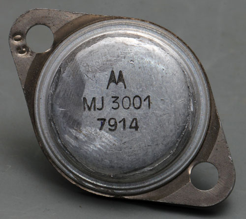
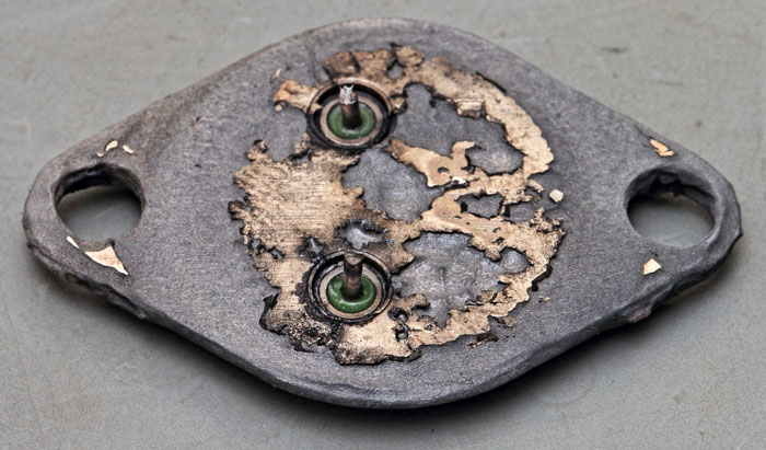
Now the Darlington MJ3001: 80V, 10A, 150W


Nothing special to see but...


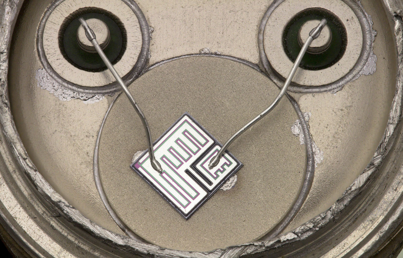
...the die is interesting!  :-+
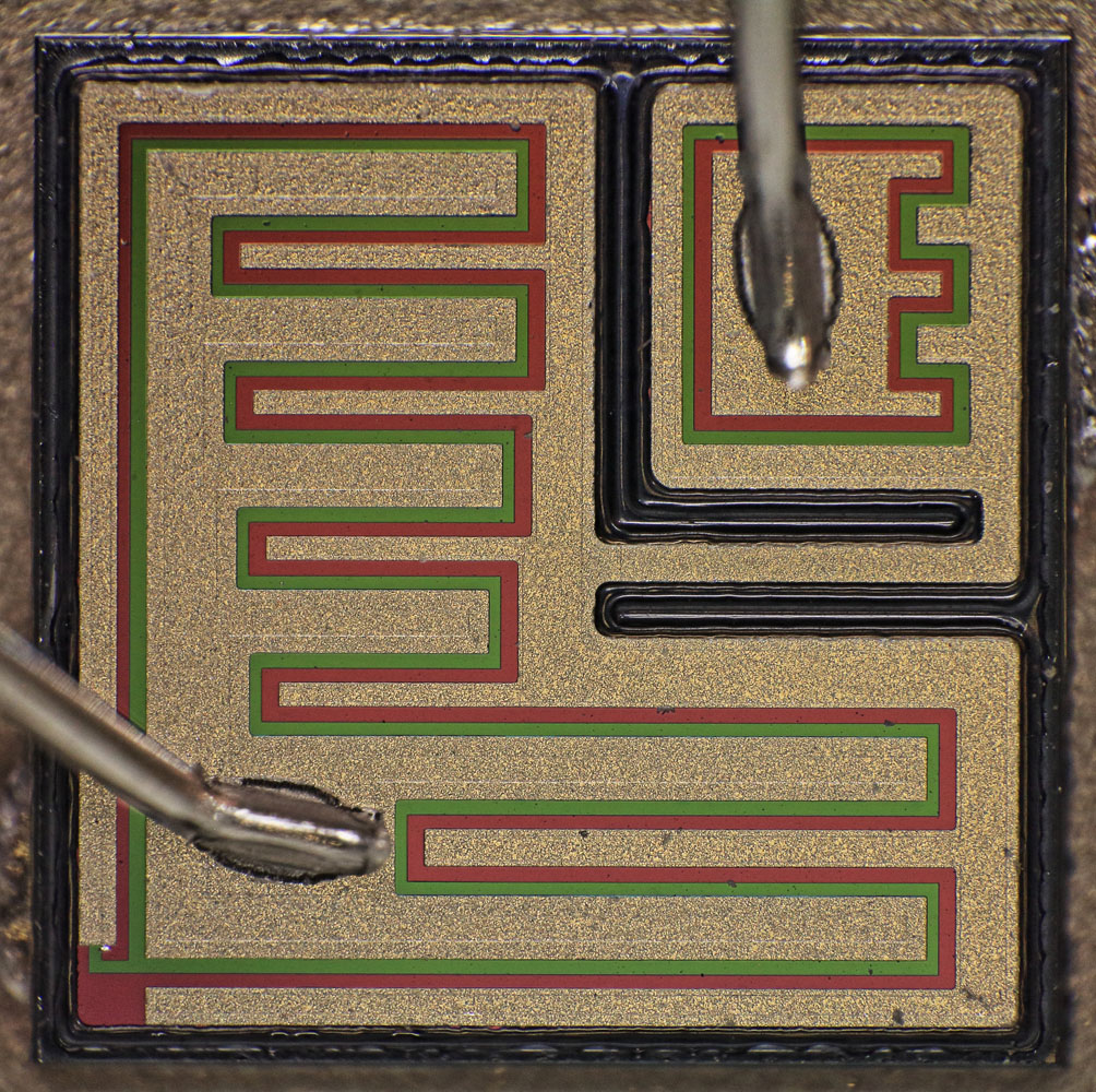
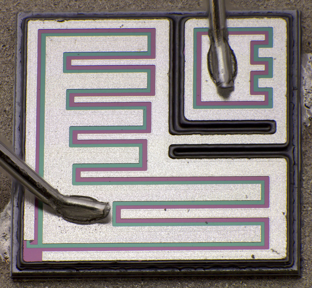
There are two trenches isolating the driver transistor.


Let´s remove the metal layer. The package got dissolved too.  >:D


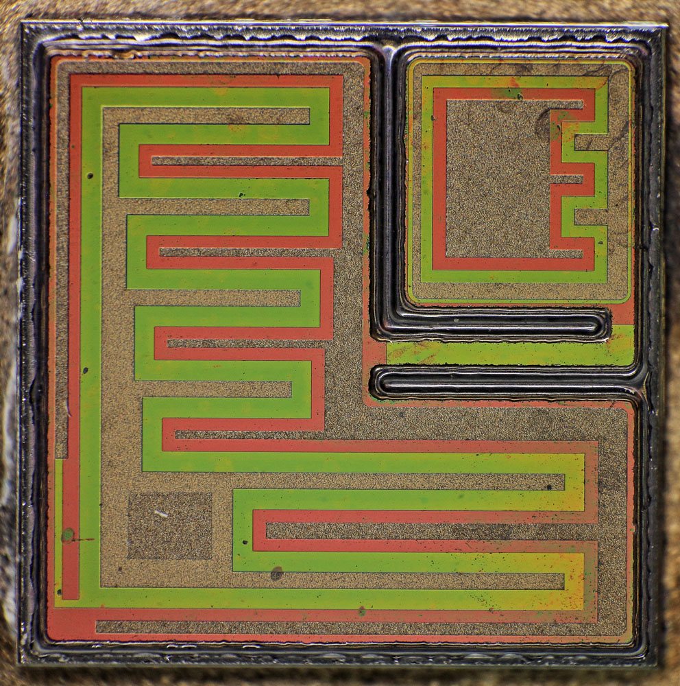
Now we see a little bit more.


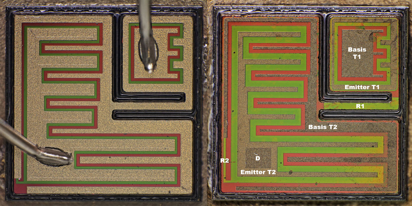
In the upper right corner we have the driver transistor. The base area in the middle of the area and the emitter like a ring around (above) it.
The metal layer connects the emitter of the driver transistor via a catwalk with the base area of the power transistor.
The power transistor is constructed like other power transistors: A base area with a emitter island above it.

You have to look closely to find the base emitter resistor R1. It is build with the red base area leading from the base area of the driver transistor, under the emitter of the driver transistor, over the catwalk to the base area of the power transistor which is connected to the emitter of the driver transistor over the metal layer.
The green area on the catwalk forms a pinch resistor to get the high resistance (2k).

The base emitter resistor R2 is built with the green emitter material of the power transistor. There is a small short stub in the lower left corner which is enough to get the 50 \$\Omega\$.

The freewheeling diode is integrated underneath the emitter bonding area. There is a opening in the emitter area so the metal layer connects to the base area which gives you the freewheeling diode from the collector to the emitter of the MJ3001.

The MJ3001 is not really built like the transistor described in the patent US2663806. The base areas are still connected.


https://www.richis-lab.de/Bipolar60.htm

 :-/O
 
The following users thanked this post: SeanB, SilverSolder, RoGeorge

Offline exe

  • Supporter
  • ****
  • Posts: 2562
  • Country: nl
  • self-educated hobbyist
Re: Transistors - die pictures
« Reply #418 on: June 12, 2021, 06:29:44 am »
I see metal layer fully covers R1. Why it doesn't short it?
 

Online NoopyTopic starter

  • Super Contributor
  • ***
  • Posts: 1734
  • Country: de
    • Richis-Lab
Re: Transistors - die pictures
« Reply #419 on: June 12, 2021, 06:36:01 am »
I see metal layer fully covers R1. Why it doesn't short it?

There is SiO2 all over the place isolating the red/green silicon. The metal layer makes contact where the greyish areas are nowhere else.  :-/O

In the greyish areas the SiO2 is opened and we see the residues of the.contact. Probably it's the rough surface we see.
 
The following users thanked this post: exe, SilverSolder

Online NoopyTopic starter

  • Super Contributor
  • ***
  • Posts: 1734
  • Country: de
    • Richis-Lab
Re: Transistors - die pictures
« Reply #420 on: June 16, 2021, 03:43:25 am »
I have added a new category:
"Thyristors and Variants"
https://www.richis-lab.de/Thyristoren.htm
I will continue to post the parts here.


General Electric 3N84, a "Thyristortetrode" also known as "Silicon Controlled Switch (SCS)".
It´s a Thyristor with a second gate.


A long time ago SCS were used in a lot of special applications like counters and ring memory but even today there is an interesting applications shown in the datasheet of the TISP83121 which is still available. With such a protection circuit you don´t deflect overvoltages (and undervoltages) into your supply like with clamping diodes but to ground. That is often a lot less problematic.


The fourth pin is connected to the can.


The die is 0,5mm x 0,5mm and looks quite similar to the 2N6027 which I have updated too: https://www.richis-lab.de/Bipolar14.htm


Understanding the different areas is no big deal.
The square in the lower right corner seems to be a testpoint for the Cathode-Gate.


https://www.richis-lab.de/Bipolar61.htm

 :-/O
 
The following users thanked this post: SeanB, doktor pyta, SilverSolder, RoGeorge

Offline David Hess

  • Super Contributor
  • ***
  • Posts: 16615
  • Country: us
  • DavidH
Re: Transistors - die pictures
« Reply #421 on: June 16, 2021, 02:13:34 pm »
A long time ago SCS were used in a lot of special applications like counters and ring memory but even today there is an interesting applications shown in the datasheet of the TISP83121 which is still available. With such a protection circuit you don´t deflect overvoltages (and undervoltages) into your supply like with clamping diodes but to ground. That is often a lot less problematic.

The same thing can be done with a bipolar transistor to redirect the current into the positive supply into ground instead, but I hardly ever see it done.  I guess the advantage of an SCS is that it latches on during the overload so there is no gate current into the positive supply.

If you did need an SCS now, a pair of bipolar transistors could be used just as with an SCR.
 

Offline mawyatt

  • Super Contributor
  • ***
  • Posts: 3263
  • Country: us
Re: Transistors - die pictures
« Reply #422 on: June 16, 2021, 03:04:41 pm »
Long ago we used 3 SCRs with core die in planes X, Y and Z as high energy detectors. These were used to "crowbar" the main power supplies when a nuclear event was detected. The idea was too quickly discharge the main energy sources in the PS before they had time to damage the main electronics in the system. During an event all the semiconductor PN junctions become forward biased and can damage the chip, this also required a minimum decoupling capacitor to limit the available energy source for the forward biased junctions. We also used large die transistors like 2N3055 as detectors. Early CMOS chips would latch up during an event, remember seeing a very expensive CMOS chip melted because of this. RCA developed a CMOS Silicon on Sapphire (SOS) process especially for radiation-hard use, later others developed Silicon on Insulator (SOI) processes for various reasons including rad hard features. Lots of time and effort went into developing techniques for equipment nuclear survivability, with different levels for different types of equipment. We had an on-site Flash Xray lab to emulate a nuclear event to help with these developments.

Thank goodness we never had to find out if all this rad-hard stuff actually worked :phew:

BTW great images as usual :-+

Best,
Curiosity killed the cat, also depleted my wallet!
~Wyatt Labs by Mike~
 

Online NoopyTopic starter

  • Super Contributor
  • ***
  • Posts: 1734
  • Country: de
    • Richis-Lab
Re: Transistors - die pictures
« Reply #423 on: June 16, 2021, 06:36:12 pm »
If you did need an SCS now, a pair of bipolar transistors could be used just as with an SCR.

 :-+


Long ago we used 3 SCRs with core die in planes X, Y and Z as high energy detectors. These were used to "crowbar" the main power supplies when a nuclear event was detected. The idea was too quickly discharge the main energy sources in the PS before they had time to damage the main electronics in the system. During an event all the semiconductor PN junctions become forward biased and can damage the chip, this also required a minimum decoupling capacitor to limit the available energy source for the forward biased junctions. We also used large die transistors like 2N3055 as detectors.

Very interesting!  :-+


We had an on-site Flash Xray lab to emulate a nuclear event to help with these developments.

I´m sure that was an interesting lab!  ;D


BTW great images as usual :-+

Thanks!  8)


Online NoopyTopic starter

  • Super Contributor
  • ***
  • Posts: 1734
  • Country: de
    • Richis-Lab
Re: Transistors - die pictures
« Reply #424 on: June 19, 2021, 06:24:12 pm »

...


I have a more recent Motorola MJ3001:


Now that is the kind of package and heatspreader we expect in more recent transistors.


The design is the same as in the older one but the die doesn´t look very good.  ???
It´s kind of dirty and in the upper left corner there is a hole in the metal layer.


https://www.richis-lab.de/Bipolar60.htm

 :-/O


Share me

Digg  Facebook  SlashDot  Delicious  Technorati  Twitter  Google  Yahoo
Smf