Author Topic: Transistors - die pictures  (Read 190922 times)

0 Members and 3 Guests are viewing this topic.

Online mawyatt

  • Super Contributor
  • ***
  • Posts: 3268
  • Country: us
Re: Transistors - die pictures
« Reply #525 on: December 27, 2021, 04:58:15 pm »
With a narrow aperture you get problems at high magnifications due to diffraction. So you better work with wide apertures, a lot of pictures and focus stacking.

But that would be cheating.

Been "cheating" for 20 years ;D

Best,
Curiosity killed the cat, also depleted my wallet!
~Wyatt Labs by Mike~
 
The following users thanked this post: firehopper

Online mawyatt

  • Super Contributor
  • ***
  • Posts: 3268
  • Country: us
Re: Transistors - die pictures
« Reply #526 on: December 27, 2021, 05:06:51 pm »

Motorola 2N3614, 35V, 7A continues, 15A peak, 77W @25°C case temperature.


There are two metal sheets contacting base and emitter which were initially connected.


There is a n-doped germanium slice acting as base region. The p-doped emitter and collector areas are alloyed into the two sides of the base slice.


There are two metal sheets. In the first place the base metal sheet is fixed by the two contact pins. The emitter metal sheet is fixed by the emitter pin and a hole in the base metal sheet. Taken together this construction assures that the emitter contact is in the middle of the germanium slice. The base metal sheet is cut at the hole where there is only one metal sheet and the cross section is lowest.


https://www.richis-lab.de/Bipolar86.htm

 :-/O

Nice 3D look!!

Well done  :clap:

Are you using Zerene for stacking?

Now it's time to really "cheat" with Stack & Stitch  >:D

Best,
« Last Edit: December 27, 2021, 05:14:32 pm by mawyatt »
Curiosity killed the cat, also depleted my wallet!
~Wyatt Labs by Mike~
 

Online mawyatt

  • Super Contributor
  • ***
  • Posts: 3268
  • Country: us
Re: Transistors - die pictures
« Reply #527 on: December 27, 2021, 05:10:50 pm »
With a narrow aperture you get problems at high magnifications due to diffraction. So you better work with wide apertures, a lot of pictures and focus stacking.
I have added 3TB to my NAS.  ;D

Exactly :-+

Best
Curiosity killed the cat, also depleted my wallet!
~Wyatt Labs by Mike~
 

Offline NoopyTopic starter

  • Super Contributor
  • ***
  • Posts: 1734
  • Country: de
    • Richis-Lab
Re: Transistors - die pictures
« Reply #528 on: December 27, 2021, 05:21:19 pm »
Thanks!

I'm using Helicon Focus for stacking. Works quite well for me.
On some pictures you can find some smaller artefacts but I won't blame the software. I often have very complex pictures: thin bondwires with small distance to big planes, hard edges and wide areas with some delicate pattern, mirroring and so on...  :phew: That isn't an easy task!

Offline David Hess

  • Super Contributor
  • ***
  • Posts: 16618
  • Country: us
  • DavidH
Re: Transistors - die pictures
« Reply #529 on: December 28, 2021, 04:39:42 am »
I may try experimenting with that since I have Magic Lantern installed which in theory supports focus bracketing on my Canon PowerShot SX150 IS that I use for macro photography.  Recently I have concentrated on getting better lighting with a ring light which helped a lot although glare has been a problem.  I need to improve the diffusion with something like a cone.
 

Offline NoopyTopic starter

  • Super Contributor
  • ***
  • Posts: 1734
  • Country: de
    • Richis-Lab
Re: Transistors - die pictures
« Reply #530 on: December 28, 2021, 07:36:39 am »
I have tried a lot of different light sources. For "small" parts like a single TO-3 a very simple but good solution is a normal sheet of paper folded like a simple tent. A common desk light gives you a very broad light with respect to small parts. The paper tent adds diffusion.
The amount of light is irrelevant if you do long term exposure. I would recommend this.
For bigger objects that's not the best solution...

Online mawyatt

  • Super Contributor
  • ***
  • Posts: 3268
  • Country: us
Re: Transistors - die pictures
« Reply #531 on: December 29, 2021, 02:05:36 am »
For smaller objects white styrofoam cups work well, but they eat lots of light and thus usually require bright LEDs or strobe/speedlight. As Noopy indicated you can use good white paper folded into a tent or rolled up into a cone. With any diffusion and various light sources be sure to do a good white balance.

A few years ago we did some modifications to a cheap IKEA LED light.

https://www.photomacrography.net/forum/viewtopic.php?f=25&t=41464&hilit=Jansjo

And a higher output Godox LED light.

https://www.photomacrography.net/forum/viewtopic.php?f=25&t=41353&p=264797&hilit=Jansjo#p264797

Best,
Curiosity killed the cat, also depleted my wallet!
~Wyatt Labs by Mike~
 

Offline NoopyTopic starter

  • Super Contributor
  • ***
  • Posts: 1734
  • Country: de
    • Richis-Lab
Re: Transistors - die pictures
« Reply #532 on: December 30, 2021, 03:59:08 pm »


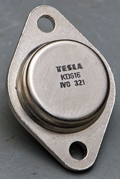
Tesla KD616, a PNP power transistor for linear applications. It´s the complementary part to the KD606.
60V, 10A, 2MHz, hfe>30 @1A


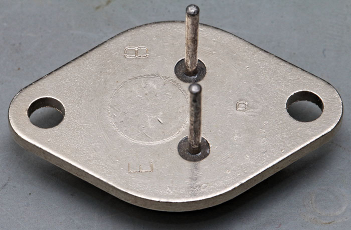
B and E, so you know where to find the right potential.  :-+


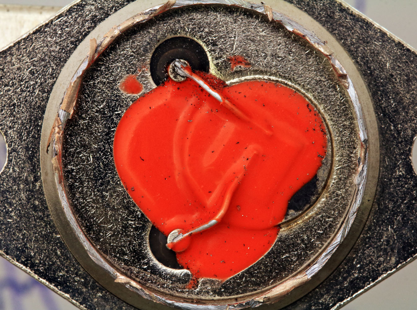
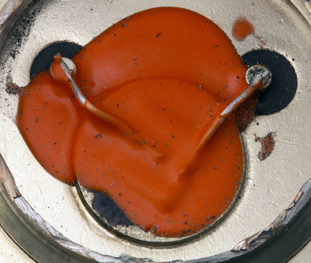
We know these Tesla transistors with the red potting.


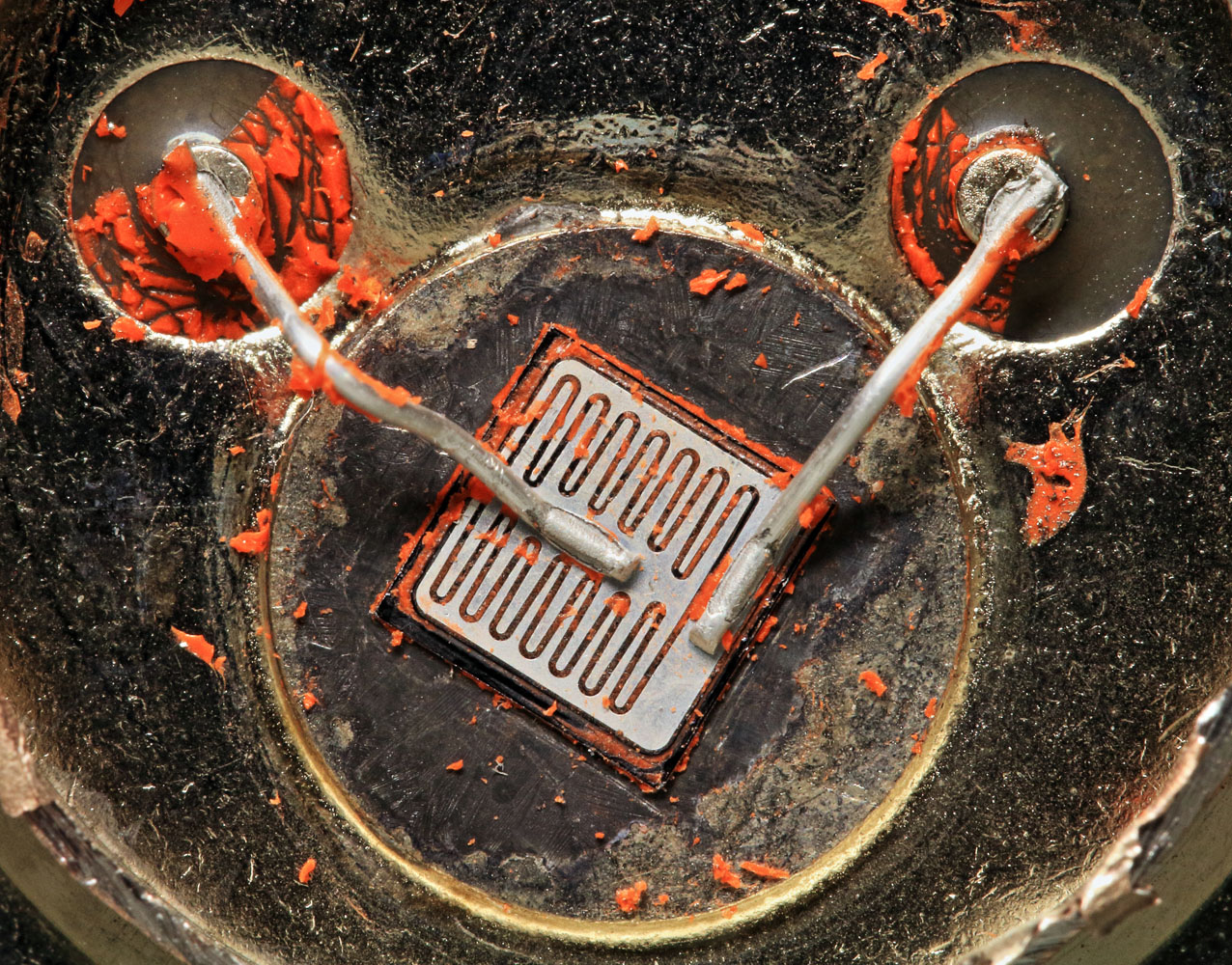
The potting doesn´t stick very hard but it´s still not easy to remove it completely.


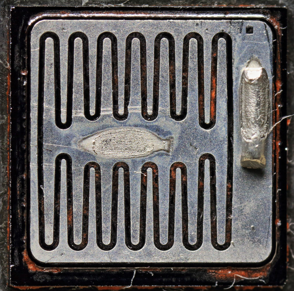
The die is quite similar to  the KD605 (https://www.richis-lab.de/Bipolar46.htm). I assume the KD60x (NPN) and the KD61x (PNP) are the same transistors just binned to different voltage ratings.


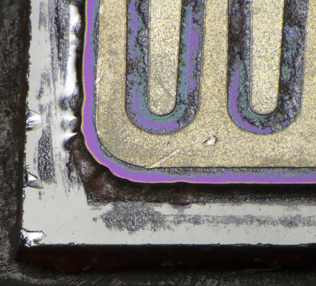
There is a square hole in the metal layer. You can see a square in the silicon underneath. This way you can check the mask alignment.


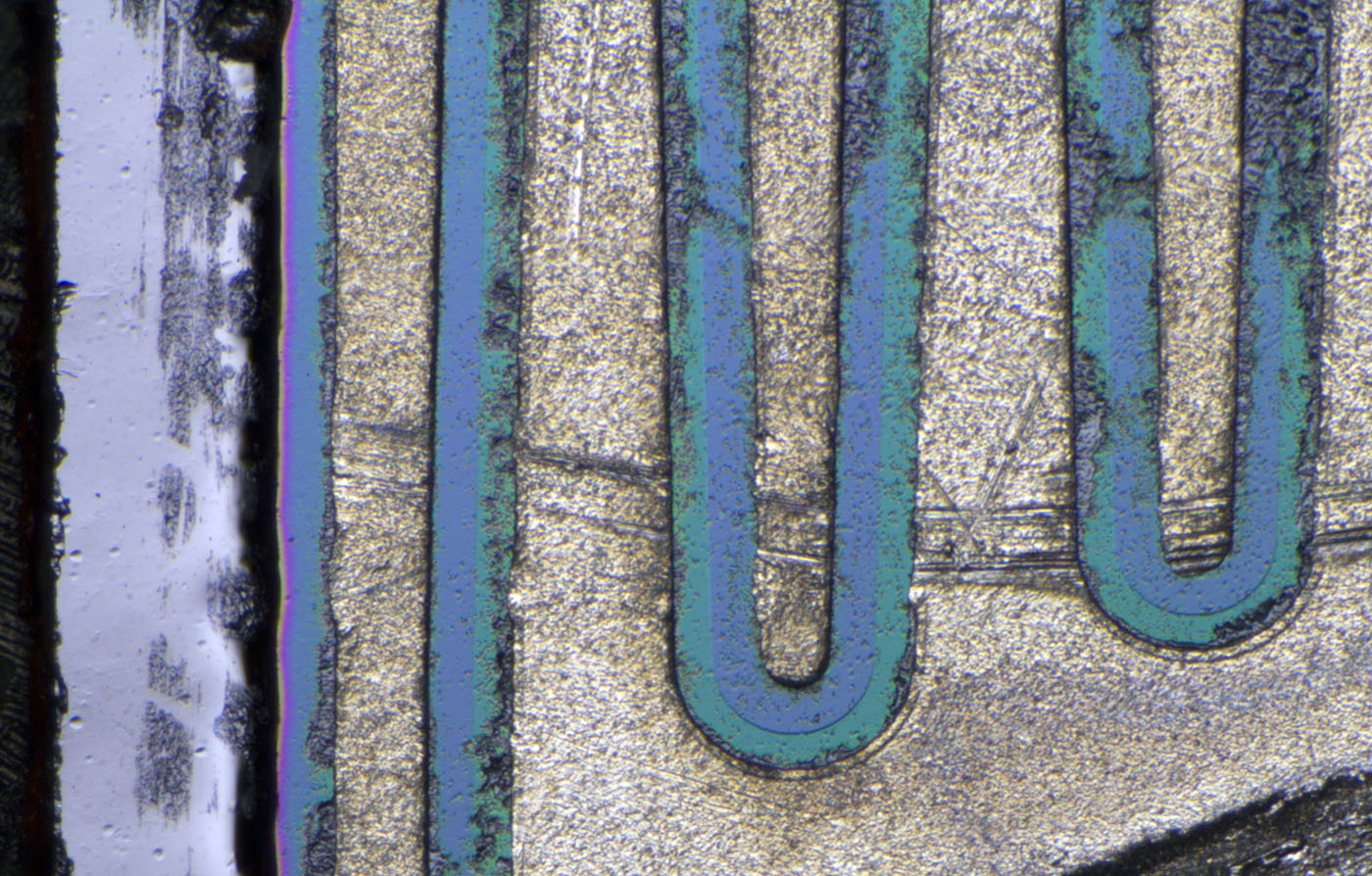
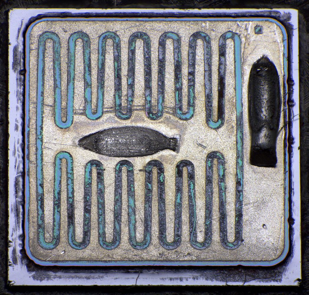
Here you can see the different colors of base and emitter. At the edges of the metal at some places you can see the step of the hole in the SiO2 isolation through which the metal can contact the silicon.
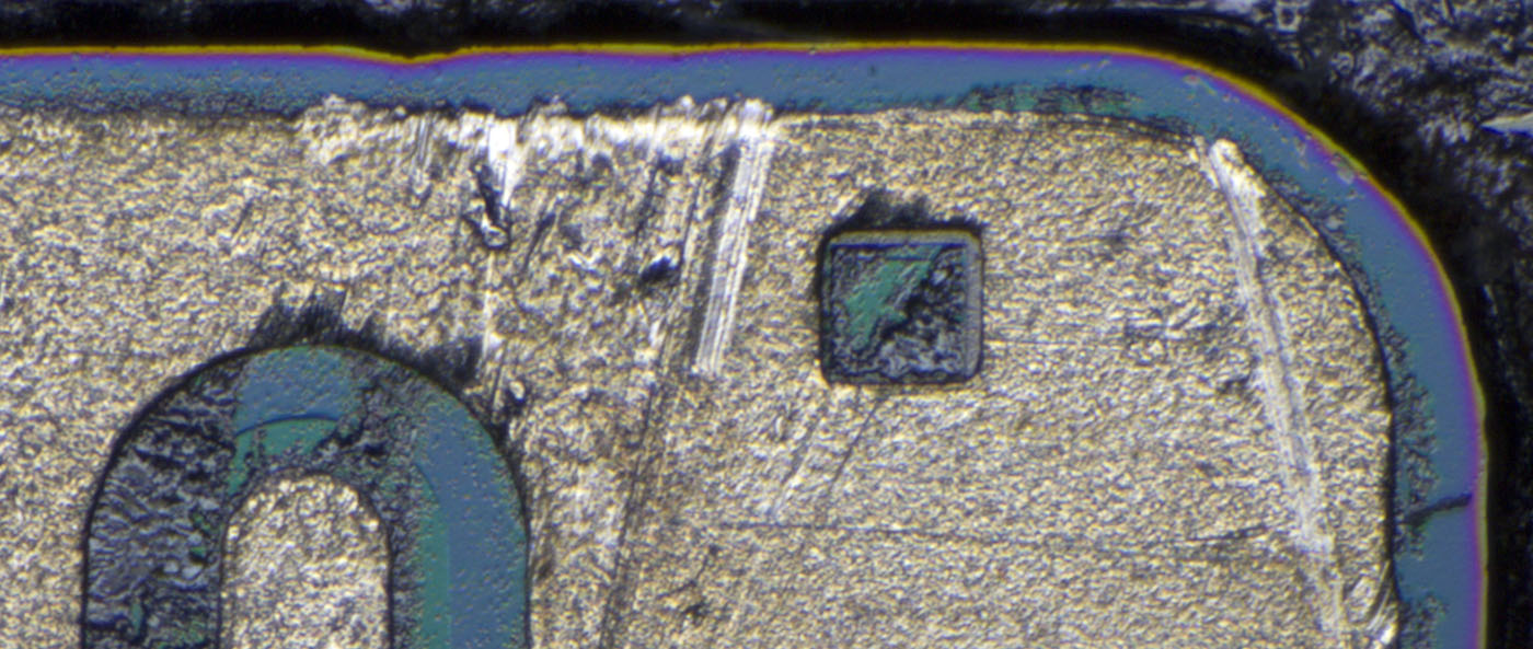
The MESA edge is quite poor compared to the KD605 (https://www.richis-lab.de/Bipolar46.htm). That´s probably due to the age. KD616 is "IV" => May 1979. KD605 is "S6" => June 1984. It seems like they have improved the process.


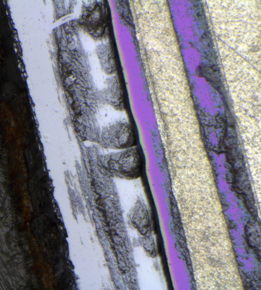
Viewed sideways you can see how inhomogeneous the etching ist.


https://www.richis-lab.de/Bipolar87.htm

 :-/O
 
The following users thanked this post: RoGeorge, Miyuki

Offline NoopyTopic starter

  • Super Contributor
  • ***
  • Posts: 1734
  • Country: de
    • Richis-Lab
Re: Transistors - die pictures
« Reply #533 on: January 07, 2022, 05:08:09 am »


The OC45 was made by a lot of companies. I don´t know which one produced this one.
Compared to the OC811 (https://www.richis-lab.de/Bipolar53.htm) the OC45 is a high frequency transistor which can switch up to 4MHz.


You can scrape off the black paint that protects the transistor against light.
In the glass housing there is a blue potting.


Looks like silicon.


You can remove the blue stuff with paint stripper.
At the transistor there are bulges around the contact wires. Perhaps there is an additional protective coating.


After the treatment with lack stripper the transistor is clean.
At the pin in the middle there is the base ring contact.


The plate is 1,4mm in diameter.


The height of the germanium plate is just 40µm.


Emitter


https://www.richis-lab.de/Bipolar88.htm

 :-/O
 
The following users thanked this post: Vgkid, doktor pyta, RoGeorge, floobydust, Miyuki

Offline exe

  • Supporter
  • ****
  • Posts: 2562
  • Country: nl
  • self-educated hobbyist
Re: Transistors - die pictures
« Reply #534 on: January 07, 2022, 07:37:11 am »
Were those devices packaged manually? I wonder how difficult it was to solder them.
 

Offline NoopyTopic starter

  • Super Contributor
  • ***
  • Posts: 1734
  • Country: de
    • Richis-Lab
Re: Transistors - die pictures
« Reply #535 on: January 07, 2022, 09:20:31 am »
I don't know for the OC45 but it seems there was a lot handcraft back in the days:
https://www.thevalvepage.com/trans/manufac/manufac1.htm
 
The following users thanked this post: SeanB

Online eutectique

  • Frequent Contributor
  • **
  • Posts: 392
  • Country: be
Re: Transistors - die pictures
« Reply #536 on: January 07, 2022, 01:55:08 pm »

The ГT906 (GT906) is a germanium power transistor that can block up to 75V. ... The second line could be a date code (1981).

It is February 1981, indeed. Soviet manufacturers used to mark production month with Roman numerals.
 
The following users thanked this post: Noopy

Online mawyatt

  • Super Contributor
  • ***
  • Posts: 3268
  • Country: us
Re: Transistors - die pictures
« Reply #537 on: January 07, 2022, 04:25:11 pm »
Interesting old transistor, great images :-+

Best,
Curiosity killed the cat, also depleted my wallet!
~Wyatt Labs by Mike~
 
The following users thanked this post: Noopy

Offline Miyuki

  • Frequent Contributor
  • **
  • Posts: 906
  • Country: cz
    • Me on youtube
Re: Transistors - die pictures
« Reply #538 on: January 11, 2022, 08:16:48 pm »
I don't know for the OC45 but it seems there was a lot handcraft back in the days:
https://www.thevalvepage.com/trans/manufac/manufac1.htm
No wonder it used to cost a fortune
 

Offline NoopyTopic starter

  • Super Contributor
  • ***
  • Posts: 1734
  • Country: de
    • Richis-Lab
Re: Transistors - die pictures
« Reply #539 on: January 11, 2022, 08:56:03 pm »
I don't know for the OC45 but it seems there was a lot handcraft back in the days:
https://www.thevalvepage.com/trans/manufac/manufac1.htm
No wonder it used to cost a fortune


Quote from: www.thevalvepage.com
The thinnest base wafers are those produced for the OC44 and OC45.These wafers are only 100 µm thick - a tenth of a millimetre. At this still quite early stage in manufacture, the dice are worth more than their weight in gold.

Sound like a lot of money but it´s just 0,05$.  ;D

Nevertheless you are absolutely right. Back in the days it was unthinkable to buy 30k transistors for 500$.

Offline NoopyTopic starter

  • Super Contributor
  • ***
  • Posts: 1734
  • Country: de
    • Richis-Lab
Re: Transistors - die pictures
« Reply #540 on: January 12, 2022, 08:15:16 pm »


I don´t know which company has built this BDY92. The marking looks a little like Philips. What is your opinion?

The BDY92 isolates 60V and can conduct 10A (15A peak). It has a "very high" transition frequency: 70MHz.


Some white potting is protecting the die.


The die is soldered on a round plate.


The edge length of the die is 3,1mm. The structure of the metal layer is interesting. I assume it shall distribute the current as good as possible while providing a low inductance.


The base emitter junction is near the emitter. I don´t know why there are two boundaries.  :-//


Driving the transistor into base-emitter-breakdown we can see the base emitter junction is near the emitter (-7,5V, 1A).


That doesn´t look good. A production problem? A damage caused by the bonding process?


And another artifact...


https://www.richis-lab.de/Bipolar89.htm

 :-/O
 
The following users thanked this post: SeanB, RoGeorge

Offline T3sl4co1l

  • Super Contributor
  • ***
  • Posts: 21686
  • Country: us
  • Expert, Analog Electronics, PCB Layout, EMC
    • Seven Transistor Labs
Re: Transistors - die pictures
« Reply #541 on: January 12, 2022, 08:18:29 pm »
Oh cool, a log periodic sort of interdigitation!  With fT of that I would expect perforated emitter, but there you have it.

Tim
Seven Transistor Labs, LLC
Electronic design, from concept to prototype.
Bringing a project to life?  Send me a message!
 

Offline David Hess

  • Super Contributor
  • ***
  • Posts: 16618
  • Country: us
  • DavidH
Re: Transistors - die pictures
« Reply #542 on: January 12, 2022, 08:51:14 pm »
That layout equalizes the emitter resistance to the far points of the emitter.
 
The following users thanked this post: RoGeorge

Offline NoopyTopic starter

  • Super Contributor
  • ***
  • Posts: 1734
  • Country: de
    • Richis-Lab
Re: Transistors - die pictures
« Reply #543 on: January 13, 2022, 09:29:53 pm »
That layout equalizes the emitter resistance to the far points of the emitter.

But compared to for example the KD616 the layout ensures a low inductance too:


Offline NoopyTopic starter

  • Super Contributor
  • ***
  • Posts: 1734
  • Country: de
    • Richis-Lab
Re: Transistors - die pictures
« Reply #544 on: January 16, 2022, 04:21:40 am »


Sescosem 391HT2 - You don´t find any information about this transistors. It is said to be similar to the BDY25: 140V, 6A, 88W, 10MHz


There is a big heatspreader.
The emitter potential is brought to the die with two bondwires.


The heatspreader is probably made out of copper. In some places it wasn´t coated probably and you can still see it.


The architecture is unusual. The inner contact is the base not the emitter and because of that the inner metal layer was made quite thin.
It seems like the die was broken out of the wafer. You can see the rough edges.


The base metal is smoother than the emitter metal. There are three edges between base and emitter. The outer two are probably the openings in the isolating SiO2. The inner one is the junction.


The base emitter breakdown voltage is quite high: -15V. The datasheet of the BDY25 states -10V.
A nice uniform glowing...  :)


https://www.richis-lab.de/Bipolar90.htm

 :-/O
 
The following users thanked this post: SeanB, exe, SilverSolder, RoGeorge

Offline NoopyTopic starter

  • Super Contributor
  • ***
  • Posts: 1734
  • Country: de
    • Richis-Lab
Re: Transistors - die pictures
« Reply #545 on: January 23, 2022, 09:38:24 pm »


Just a small signal transistor, a SC206 built in the Halbleiterwerk Frankfurt Oder.
15V, 100mA, 200mW, 300MHz


The naming is a little strange. S stands for silicon. Since they didn´t package germanium transistors in plastic packages the S is omitted. They omitted the 2 too and so there is just a C06.  :-//

The transistors were binned by hfe. That´s the E in the upper left corner. They sold B (28-71) - F (450-1120). C is a very short datecode.


The edge length of the die is 0,5mm. It is quite similar to the SF137 (https://www.richis-lab.de/Bipolar75.htm).


https://www.richis-lab.de/Bipolar91.htm

 :-/O
 
The following users thanked this post: SeanB, RoGeorge, capt bullshot

Offline NoopyTopic starter

  • Super Contributor
  • ***
  • Posts: 1734
  • Country: de
    • Richis-Lab
Re: Transistors - die pictures
« Reply #546 on: January 27, 2022, 07:36:29 pm »


Sescosem BDX18, a PNP transistor conducting up to 15A with a Vce of 60V. ft is 4MHz. The package can dissipate up to 117W.


The die is placed on a big heatspreader and potted.


The potting is really hard to remove. It´s a MESA transistor.


In the lower left corner there is a strange discoloration.  :-//


https://www.richis-lab.de/Bipolar92.htm

 :-/O
 
The following users thanked this post: SeanB, RoGeorge

Offline doktor pyta

  • Frequent Contributor
  • **
  • Posts: 488
  • Country: pl
Re: Transistors - die pictures
« Reply #547 on: January 29, 2022, 12:17:32 pm »
Just found this.
 
The following users thanked this post: RoGeorge, Noopy

Offline NoopyTopic starter

  • Super Contributor
  • ***
  • Posts: 1734
  • Country: de
    • Richis-Lab
Re: Transistors - die pictures
« Reply #548 on: January 29, 2022, 12:43:02 pm »

Offline NoopyTopic starter

  • Super Contributor
  • ***
  • Posts: 1734
  • Country: de
    • Richis-Lab
Re: Transistors - die pictures
« Reply #549 on: February 03, 2022, 08:12:48 pm »


One more Miniplast-Transistor built by the Halbleiterwerk Frankfurt Oder. The SF216 is specified for high frequency amplifiers and oscillators up to 100MHz. Compared to the SC206 (https://www.richis-lab.de/Bipolar91.htm) the SF216 offers a noticeably higher reverse voltage of 33V. The maximum permissible collector current is 100mA. The cutoff frequency is specified with 350MHz. The D in the upper left corner stands for a hfe between 112 and 280.


The edge length of the dies is 0,5mm. The structures are quite similar to the SC206 (https://www.richis-lab.de/Bipolar91.htm), but in fact they are a bit closer to the SF137 (https://www.richis-lab.de/Bipolar75.htm). In the left lower corner there is a pattern to check the mask alignment.


https://www.richis-lab.de/Bipolar93.htm

 :-/O
 
The following users thanked this post: SeanB, RoGeorge


Share me

Digg  Facebook  SlashDot  Delicious  Technorati  Twitter  Google  Yahoo
Smf