Author Topic: Transistors - die pictures  (Read 191207 times)

0 Members and 2 Guests are viewing this topic.

Offline David Hess

  • Super Contributor
  • ***
  • Posts: 16620
  • Country: us
  • DavidH
Re: Transistors - die pictures
« Reply #550 on: February 03, 2022, 10:18:34 pm »
I would like to see what a Zetex "super e-line" transistor looks like.  Other manufacturers now make them as low saturation voltage and high current gain parts.
 

Offline NoopyTopic starter

  • Super Contributor
  • ***
  • Posts: 1734
  • Country: de
    • Richis-Lab
Re: Transistors - die pictures
« Reply #551 on: February 04, 2022, 05:20:56 am »
I would like to see what a Zetex "super e-line" transistor looks like.  Other manufacturers now make them as low saturation voltage and high current gain parts.

I will put it on the list.  :-+
 
The following users thanked this post: SeanB

Offline floobydust

  • Super Contributor
  • ***
  • Posts: 7000
  • Country: ca
Re: Transistors - die pictures
« Reply #552 on: February 04, 2022, 08:54:09 pm »
ZTX689B and ZTX851 are popular not as a medium power transistor, but for low noise audio preamplifiers and they have a low rbb'. The die would be very interesting to see.
 
The following users thanked this post: Wolfgang

Offline NoopyTopic starter

  • Super Contributor
  • ***
  • Posts: 1734
  • Country: de
    • Richis-Lab
Re: Transistors - die pictures
« Reply #553 on: February 04, 2022, 09:00:42 pm »
ZTX689B and ZTX851 are popular not as a medium power transistor, but for low noise audio preamplifiers and they have a low rbb'. The die would be very interesting to see.

 :-+

Offline David Hess

  • Super Contributor
  • ***
  • Posts: 16620
  • Country: us
  • DavidH
Re: Transistors - die pictures
« Reply #554 on: February 05, 2022, 01:38:17 am »
ZTX689B and ZTX851 are popular not as a medium power transistor, but for low noise audio preamplifiers and they have a low rbb'. The die would be very interesting to see.

All of the "super e-line" style transistors should have low base spreading resistance.

The way I remember it, Zetex bought obsolete IC fabrication equipment which was still higher performance than what was being used for bipolar power transistors, so they were able to take advantage of an advanced design, but it was never clear to me what was actually different about their transistors.  I do not think they are just another perforated emitter design.
 
The following users thanked this post: exe

Offline NoopyTopic starter

  • Super Contributor
  • ***
  • Posts: 1734
  • Country: de
    • Richis-Lab
Re: Transistors - die pictures
« Reply #555 on: February 05, 2022, 07:49:14 pm »


Tesla OC26, a germanium transistor supplying you with 32V, 3,5A, 12,5W and a hfe of 20-75.
The OC27 is specified with a hfe of 60-180. The other characteristics are the same as for the OC26. These transistors were probably binned.


The thickness of the base plate is 3,1mm!  :o


The small cylinder probably dehumidifies the package.


The contacts are metal sheets welded to the pins of the package.


The base metal sheet forms a ring carrying the germanium slice.
It seems like the transistor was coated with some clear varnish.


At the edge the germanium slice is round about 200µm thick.


Here you can see the socket on which the transistor is mounted.


https://www.richis-lab.de/Bipolar94.htm

 :-/O
 
The following users thanked this post: RoGeorge, Miyuki

Offline NoopyTopic starter

  • Super Contributor
  • ***
  • Posts: 1734
  • Country: de
    • Richis-Lab
Re: Transistors - die pictures
« Reply #556 on: February 06, 2022, 04:29:40 am »


Sescosem 391HT2 - You don´t find any information about this transistors. It is said to be similar to the BDY25: 140V, 6A, 88W, 10MHz

[...]

https://www.richis-lab.de/Bipolar90.htm

Someone told me he knows the 391HT2 as a soviet transistor (it would be a 391NT2).
He had a picture of the 391HT2 with a Russian manufacturer logo.

Sescosem naming a transistor like a soviet transistor? I have never seen something like that.
A Russian manufacturer naming a transistor like a Sescosem transistor? I can´t believe that too.

What is your opinion?

Offline Ground_Loop

  • Frequent Contributor
  • **
  • Posts: 645
  • Country: us
Re: Transistors - die pictures
« Reply #557 on: February 06, 2022, 03:05:42 pm »
Not as good as most here, but thought this was really interesting. The attached was removed from a failed variable frequency drive. This wafer contains 7 IGBTs (rated 1200 volts and 18 amps each) with protection diodes. Six of them are the output bridge to the motor and the seventh is a brake resistor chopper. Also on the wafer are the six diodes that rectify the incoming 3 phase 480VAC.  The small device on the far right is the temperature feedback.  The six black IGBTs suffered catastrophic failure due to sudden power disconnect combined with improper line conditioning. 

Attachments between the device and the circuit board are through a block of pogo pins bolted to the top. The bolt connection also serves to attach the wafer against the heat sink. The whole wafer is coated in silicone gel that the pogo pins penetrate for connections. The silicone gel was tough to remove. Seems that nothing is a good solvent for it. Persistence with 3 in 1 oil and an acid brush removed enough for the picture.

1402544-0
« Last Edit: February 06, 2022, 03:08:29 pm by Ground_Loop »
There's no point getting old if you don't have stories.
 
The following users thanked this post: RoGeorge

Offline NoopyTopic starter

  • Super Contributor
  • ***
  • Posts: 1734
  • Country: de
    • Richis-Lab
Re: Transistors - die pictures
« Reply #558 on: February 07, 2022, 03:36:22 pm »
 :-+
Silicone gel potting is a pain in the ass!  :rant:

Offline NoopyTopic starter

  • Super Contributor
  • ***
  • Posts: 1734
  • Country: de
    • Richis-Lab
Re: Transistors - die pictures
« Reply #559 on: February 18, 2022, 04:24:00 am »


Tungsram ASZ1017, a Germanium based PNP power transistor.

There are four transistors: ASZ1015, ASZ1016, ASZ1017 and ASZ1018. All of them with a maximum power dissipation of 20W, a maximum collector current of 6A and a ft of 250kHz. Vce of the ASZ1015 is 60V. The others are specified with 32V to 48V depending on the datasheet you look at. The transistors have different amplification factors. The ASZ1017 is specified with 25 to 75.

It seems like ASZ1015 - ASZ1018 are worse variants of the ASZ15 - ASZ18. The ASZ15 - ASZ18 can conduct up to 8A and the maximum power dissipation is 30W.


The base plate of the transistor is quite thick.


There is a notch in the base plate.


The package is full with a dehumidifier powder.


The setup is quite similar to the other transistors we have seen. Base and emitter contact was one sheet in the beginning. In contrast to the other transistors here the sheet was cutted mechanically.


Nothing too special...


https://www.richis-lab.de/Bipolar95.htm

 :-/O
 
The following users thanked this post: SeanB, RoGeorge

Offline NoopyTopic starter

  • Super Contributor
  • ***
  • Posts: 1734
  • Country: de
    • Richis-Lab
Re: Transistors - die pictures
« Reply #560 on: February 21, 2022, 07:34:33 am »
A small update to the Tungsram ASZ1017:


The case is made of plated copper. The dome on which the germanium plate is placed was not plated.

In the second picture you can see that the germanium plate is a square. It´s round about 0,2mm thick.


https://www.richis-lab.de/Bipolar95.htm#Update

 :-/O
 
The following users thanked this post: SeanB, SilverSolder, RoGeorge, Miyuki

Offline SilverSolder

  • Super Contributor
  • ***
  • Posts: 6126
  • Country: 00
Re: Transistors - die pictures
« Reply #561 on: February 21, 2022, 02:43:27 pm »

OMG your pictures keep getting more amazing!  :D
 
The following users thanked this post: Noopy

Offline NoopyTopic starter

  • Super Contributor
  • ***
  • Posts: 1734
  • Country: de
    • Richis-Lab
Re: Transistors - die pictures
« Reply #562 on: February 25, 2022, 11:16:28 am »


RCA 2N3773, a very powerful transistor (140V, 16A/30A, 150W).

There is a smaller brother (2N4348) and a bigger brother (2N6259). The latter with 170V/250W.

Datasheet states a hfe of 15-60.


A big heatspreader and quite big contact sheets compared to for example the 2N3055H (https://www.richis-lab.de/2N3055_05.htm).


The edge length of the die is 6,3mm to make the high current rating possible.


It´s a hometaxial transistor as it is explained with the "2N3055 (1966)" in more detail: https://www.richis-lab.de/2N3055_08.htm


Typical for a hometaxial transistor the base emitter breakdown occurs quite late: -34V

At 1A the current distribution is very uneven.


Increasing the current to 3A (>100W of power) kills the junction.

I have done a video: https://www.richis-lab.de/images/transistoren/a45x09.mp4  >:D


 >:D


https://www.richis-lab.de/Bipolar96.htm

 :-/O
 
The following users thanked this post: SeanB, SilverSolder, RoGeorge, capt bullshot

Offline NoopyTopic starter

  • Super Contributor
  • ***
  • Posts: 1734
  • Country: de
    • Richis-Lab
Re: Transistors - die pictures
« Reply #563 on: March 07, 2022, 04:51:22 am »


2SD70 is a power transistor built by NEC. We don´t see "NEC" on the package but the special construction makes it likely that it is really built by NEC.

There is few information about the transistor. Looks like it can conduct 2A and isolate 25V. The TO-66 package allows you to dissipate up to 15W.


That´s a strange construction...


There are brackets welded on the pins which makes it easier to bond the connection wires.


The die looks quite normal (1,2mm x 1,2mm). You have two base contact areas so you can turn the die 180°.


Nothing special...


But in the upper left corner it looks like the metal migrated a little to the junction or it wasn´t removed properly while manufacturing the transistor.


Base emitter breakdown at -7,5V / 10mA.


100mA - It seems like the "metal problem" doesn´t affect the current distribution.


200mA


500mA


https://www.richis-lab.de/Bipolar97.htm

 :-/O
 
The following users thanked this post: SeanB, exe, SilverSolder, RoGeorge, capt bullshot, ch_scr

Offline NoopyTopic starter

  • Super Contributor
  • ***
  • Posts: 1734
  • Country: de
    • Richis-Lab
Re: Transistors - die pictures
« Reply #564 on: March 21, 2022, 04:41:39 am »


Hitachi 2SB228, a Ge-Transistor conducting up to 5A with an Vce of 35V. At 25°C it can dissipate up to 50W.


The thickness of the base plate is 1,3mm. There is a circle...


There is some dehumidifier.


The transistor itself is placed on a socket as we have seen it a lot.

There is an opaque protection paint.


Most of the germanium transistors use solder to connect emitter and collector and in addition to p-dope the n-doped germanium disc.

Here the connector wire of the emitter is soldered to a round metal plate. The p-doping has to be under this metal plate.


Now that is another Hitachi 2SB228.


But the base plate is really thin (0,85mm)!


Now that´s the cause for the thinner base plate. Hitachi has put a massive heatspreader into the package. There is hardly room left for the dehumidifier.

This transistor is probably as good as the upper one but if you look at it from the outside it looks like a worse one.


The protection paint looks a little worse than in the first transistor.


https://www.richis-lab.de/Bipolar98.htm

 :-/O
 
The following users thanked this post: SeanB, SilverSolder, RoGeorge, Miyuki

Offline Richard576

  • Newbie
  • Posts: 9
  • Country: nl
Re: Transistors - die pictures
« Reply #565 on: March 25, 2022, 12:12:12 am »
I have been following your topic for a while, very interesting to the point that a few days ago i decided to open a old ussr transistor which came from my broken old 70's oscilloscope, i guess it is germanium, the writing on it is cyrillic it is to-3 size but without the mounting tabs, it has been standing in sight on a ledge for years and a few days ago i was bored to the point i thought "now is the time, i wanna see whats inside", just like you  :-+

Opening it i found the white powder which you refer to as dehumidifier which makes sense if there is a little bit of it in a transistor
On the other hand: mine was completely packed with bright white powder , could that be to transfer heat?, and could that be the dreaded beryllium oxide in powdered form?  :palm:

As you may guess and notice: i am a bit freaked out, i did not expect the white powder as most of the transistors you open do not have it, i have seen one fully packed and the powder looks different to mine, mine is very fine structure like talcum powder en bright white.

I tossed the whole bunch in a box outside, cleaned my workspace until my fingers where raw, showered an hour and washed my clothes 3 times, just to be sure...  ::)

Any thoughts on this?

Richard , netherlands
« Last Edit: March 25, 2022, 12:44:29 am by Richard576 »
 

Offline NoopyTopic starter

  • Super Contributor
  • ***
  • Posts: 1734
  • Country: de
    • Richis-Lab
Re: Transistors - die pictures
« Reply #566 on: March 25, 2022, 04:56:17 am »
Hi Richard!

You don't have to worry about that powder. That surely was a dehumidifier.
It would just make no sense to fill a package with BeO powder. The heat transfer through the base plate of the package is quite good. That would be like wrapping a copper busbar with aluminium foil to reduce the resistance.
I'm not even sure if the thermal conductivity of BeO powder is that good.

You are just in danger to damage your clothes by too much washing.  ;)

Greetings,

Richard

Offline Richard576

  • Newbie
  • Posts: 9
  • Country: nl
Re: Transistors - die pictures
« Reply #567 on: March 25, 2022, 12:23:54 pm »
Hi Richard!

Thank you so much for your answer, this had me spooked , i can breathe again  :-DD :-+

I will hang upside down in my garbage container to get it out if i can find it, i will post some picture if i can.
Do you think the desiccant is something usually in germanium transistors found as i understood these are very susceptible to moisture ingress and damage, the indium solder becomes damaged?
I cant remember a photo of you with a silicium transistor with desiccant inside?

As i am new to this i guessed mine being old it was probably soldered shut and so i tried to heat it hoping the solder would melt, i now know they are probably welded in some form so you need to dremel them open, but in the heating i destroyed the text on it so no idea what type it is/was  :(

Thanks a bunch and i will post some photos soon.
Big kudos for your topic, i find this so interesting and amazing technology  :-+
 

Offline NoopyTopic starter

  • Super Contributor
  • ***
  • Posts: 1734
  • Country: de
    • Richis-Lab
Re: Transistors - die pictures
« Reply #568 on: March 25, 2022, 06:07:44 pm »
There is no passivation on a germanium transistor so they are especially susceptible to moisture. But I don´t know what the precise damage szenario is.

You can find dehumidifier in silicon transistors too: https://www.richis-lab.de/Bipolar31.htm
They all have to protect their semiconductor structures. If your passivation is not good enough or your package isn´t tight enough you have to put dehumidifier into the package. If it is really bad even a dehumidifier doesn´t help: https://www.richis-lab.de/Bipolar65.htm

Thanks for the positive feedback. I´m planning to open "some" more parts...  ;D :-+

Offline Richard576

  • Newbie
  • Posts: 9
  • Country: nl
Re: Transistors - die pictures
« Reply #569 on: March 29, 2022, 12:01:27 am »
I understand about passivation but would that be passivation of the metal parts? I guess there is not much point in passivating germanium or silicon?

Anyway, unfortunately i could not retrieve my transistor of the bottom of the garbage can, my girlfriend tossed the contents of the bag-less vacuum cleaner on top of it and i am not looking forward to wonder through a few pounds of vacuum cleaner dust and crap, sorry  :--
It wasn't all that exciting also just a piece of germanium with 2 contact points on it.

Thanks for now, looking forward to the opening of other packages  :-+
 

Offline NoopyTopic starter

  • Super Contributor
  • ***
  • Posts: 1734
  • Country: de
    • Richis-Lab
Re: Transistors - die pictures
« Reply #570 on: March 29, 2022, 06:11:10 am »
I understand about passivation but would that be passivation of the metal parts? I guess there is not much point in passivating germanium or silicon?

Especially the semiconductor material has to be protected with a passivation layer!
Back in the days one important step of the manufacturing process was etching the surface of a diode or transistor to get it as clean as possible. (Today "everything is clean all the time".  ;) )
Surface contamination is a critical issue. Very very little contamination can ruin your device. That's why there were MESA transistors and why the best zener diodes are buried.


Anyway, unfortunately i could not retrieve my transistor of the bottom of the garbage can, my girlfriend tossed the contents of the bag-less vacuum cleaner on top of it and i am not looking forward to wonder through a few pounds of vacuum cleaner dust and crap, sorry  :--
It wasn't all that exciting also just a piece of germanium with 2 contact points on it.

Sounds quite normal.  :-+

Offline NoopyTopic starter

  • Super Contributor
  • ***
  • Posts: 1734
  • Country: de
    • Richis-Lab
Re: Transistors - die pictures
« Reply #571 on: April 01, 2022, 07:49:55 pm »


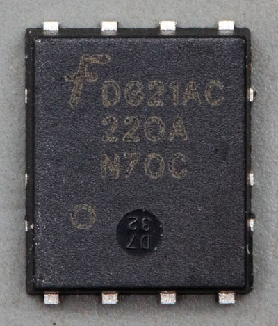
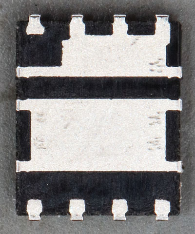
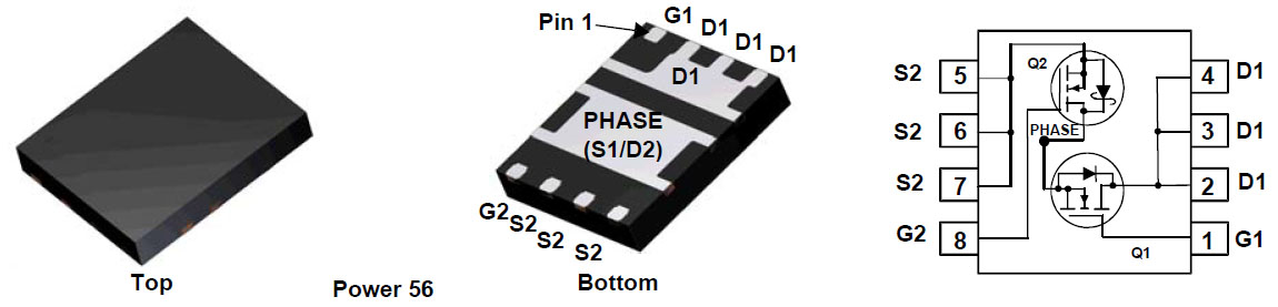
Now let us take a look into a more up to date transistor! The Fairchild FDMS3602S offers two asymmetric n-channel MOSFETs in a low-profile Power 56 package. The design is optimized for a buck converter. Transistor Q1 is the switching transistor. Q2 is the active rectifier. The integration in a package allows us to keep the traces short that carry switched currents. That reduces losses due to parasitic inductances and EMC problems.

The transistors own significantly different specs. Breakdown voltage is 25 for both transistors. Q1 offers a maximum on resistance of 8.1mΩ. The resistance of Q2 is significantly smaller with a maximum of 3.4mΩ. This is advantageous when the input voltage of a buck regulator is more than twice the output voltage. In this case, Q2 conducts current longer than Q1 and contributes more to the total loss. The datasheet states a permanent current carrying capability of 30A/40A (Q1/Q2, Tc=25°C). Up to 40A/100A are allowed for a short time.

The switching transistor Q1 has a higher impedance, but offers lower capacitances and faster switching. The rise and fall times are typically half those of Q2. This reduces switching losses in Q1 which is loaded with the input voltage.

As being the active rectifier Q2 has a Schottky diode connected in parallel to the intrinsic body diode. The lower forward voltage and smaller reverse capacitance reduce losses in the dead times when both transistors are blocked and in the transition phases. One could use the Schottky diode without driving the transistor. However the datasheet points out that typically for a Schottky diode the reverse current increases sharply with temperature. That can cause problems with the maximum power dissipation of the package. The Schottky diode is not a discrete element, but is located within the PowerTrench MOSFET. Fairchild calls these components SyncFETs.


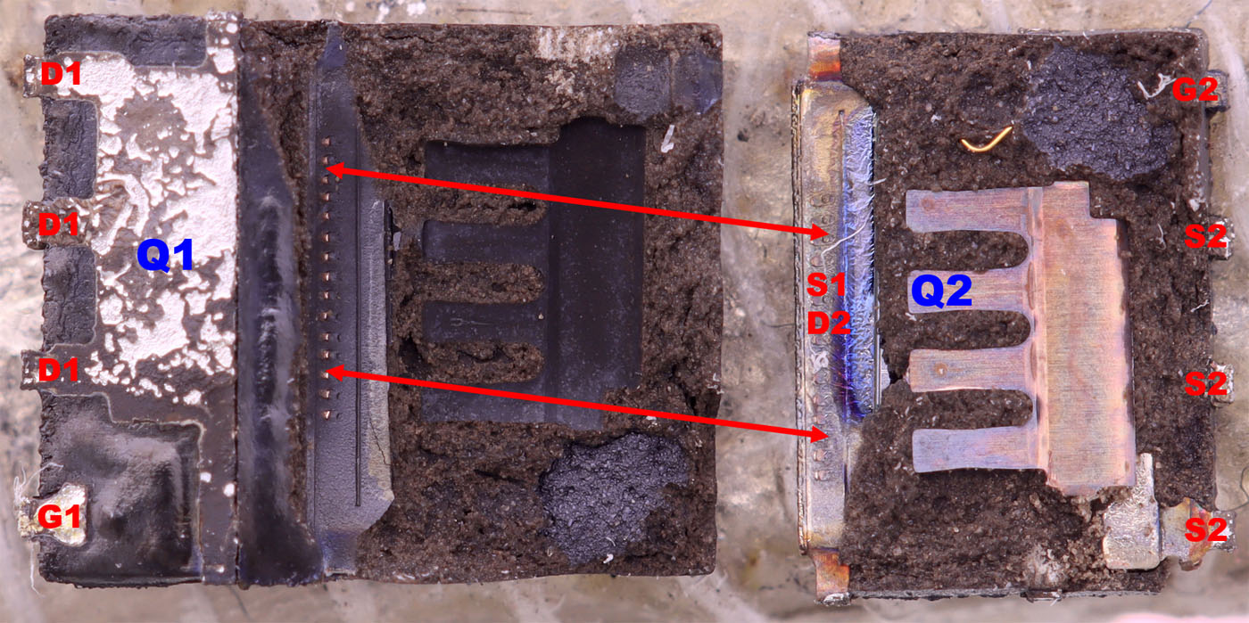
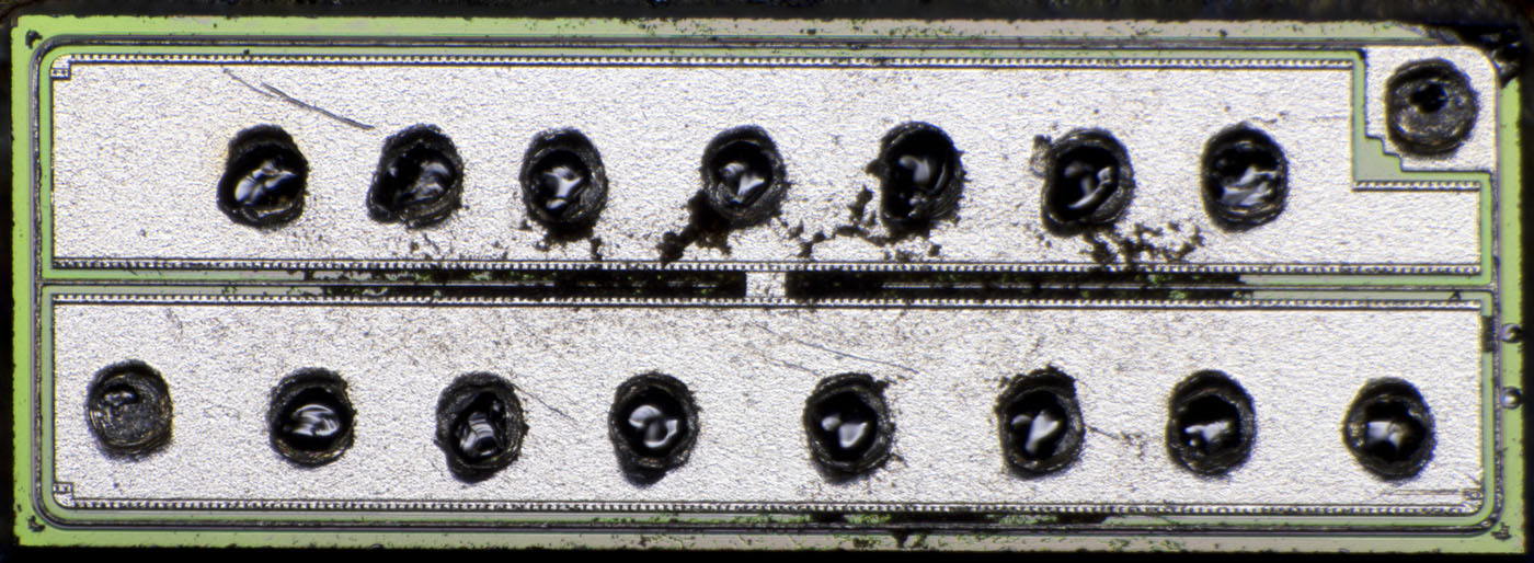
The transistor Q1 is located on the left leadframe. 15 bondwires connect the top of the transistor (source) with the leadframe in the middle. Q2 is placed here. Source of Q2 is connected with a comb-like sheet metal element. Above this contact sheet you can see the bondwire which connects the gate.


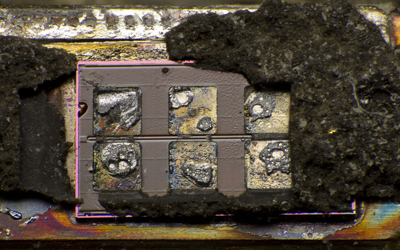
Q1 is 2.1mm x 0.8mm. The source metal layer is divided into two areas.

Vias are visible just at the upper and lower edges of these areas. Most likely the MOSFET consists of many small MOSFET cells as it is common for power MOSFETs (see for example BUK446: https://www.richis-lab.de/FET07.htm). It is interesting that vias can just be seen on the sides.

The gate potential arrives in the upper right corner and is distributed over the die with a thin frame structure.


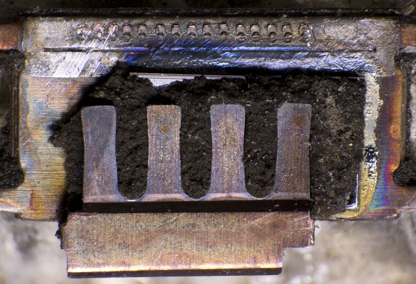
Q2 is 2.5mm x 1.5mm. The contact plate has four contact fingers but just three of them are connected to the die. Apparently this contact element is suitable for contacting wider MOSFETs.

The surface is covered with a protective layer, probably a polyimid. In the middle, at the upper and lower edge thin gate traces can be seen.


https://www.richis-lab.de/FET22.htm

 :-/O
 
The following users thanked this post: SeanB, SilverSolder, RoGeorge, Miyuki

Online T3sl4co1l

  • Super Contributor
  • ***
  • Posts: 21688
  • Country: us
  • Expert, Analog Electronics, PCB Layout, EMC
    • Seven Transistor Labs
Re: Transistors - die pictures
« Reply #572 on: April 01, 2022, 08:11:25 pm »
Cool!  ...Aww, was hoping to see what the schottky structure looks like.  But it's buried under all that metal, of course. ::) Oh well :)

Tim
Seven Transistor Labs, LLC
Electronic design, from concept to prototype.
Bringing a project to life?  Send me a message!
 

Online Miyuki

  • Frequent Contributor
  • **
  • Posts: 907
  • Country: cz
    • Me on youtube
Re: Transistors - die pictures
« Reply #573 on: April 03, 2022, 01:42:20 pm »
Great work
I just wonder if can be opened some of this integrated high power buck for high power processors
Like for example
TPS546D24A

As they work with huge currents and in single MHz switching frequencies
 

Offline NoopyTopic starter

  • Super Contributor
  • ***
  • Posts: 1734
  • Country: de
    • Richis-Lab
Re: Transistors - die pictures
« Reply #574 on: April 03, 2022, 05:39:31 pm »
Thanks!  :)

You are right the TPS546D24A sounds interesting! I will put it on my (long) list.  :-+

Also on my list is a LT8638. It gives you just 10A/12A but integrated in the LQFN package there are one 100nF and two 10nF capacitors!  :o
Either they integrated MLCCs or there are Silicon Capacitors in the package.
 
The following users thanked this post: Miyuki


Share me

Digg  Facebook  SlashDot  Delicious  Technorati  Twitter  Google  Yahoo
Smf