Author Topic: Transistors - die pictures  (Read 191434 times)

0 Members and 2 Guests are viewing this topic.

Online NoopyTopic starter

  • Super Contributor
  • ***
  • Posts: 1735
  • Country: de
    • Richis-Lab
Re: Transistors - die pictures
« Reply #625 on: August 24, 2022, 04:13:26 pm »
Interesting!

I don't know what is going on there. Perhaps the additional sheet makes it easier to weld the two parts?

Online T3sl4co1l

  • Super Contributor
  • ***
  • Posts: 21693
  • Country: us
  • Expert, Analog Electronics, PCB Layout, EMC
    • Seven Transistor Labs
Re: Transistors - die pictures
« Reply #626 on: August 24, 2022, 04:35:46 pm »
Yeah could be something like that, a diffusion barrier, or a bonding aid (filler?), or both.

Aluminum in particular cannot be bonded to gold (due to formation of an especially brittle intermetallic), but a more compatible or more resistant metal could be used.  I'm not sure what, offhand; not nickel either, as that has the same problem; tin is well-behaved with both, but that's just a soldered joint and may not be strong enough; iron may be okay (intermetallic is still formed, but a harder one, in a thinner interface layer I think, and importantly, it won't tend to degrade over time as for more mobile ions (lower melting substances)); or perhaps harder/refractory metals are used -- I don't know about say chromium or molybdenum, but maybe aluminum just acts like solder on them, not reacting enough to matter?

If you ever get the opportunity to drop it in front of an XRD analyzer, that should tell something. ;D

Tim
Seven Transistor Labs, LLC
Electronic design, from concept to prototype.
Bringing a project to life?  Send me a message!
 
The following users thanked this post: Noopy, karpouzi9

Online NoopyTopic starter

  • Super Contributor
  • ***
  • Posts: 1735
  • Country: de
    • Richis-Lab
Re: Transistors - die pictures
« Reply #627 on: August 24, 2022, 04:52:48 pm »
If you ever get the opportunity to drop it in front of an XRD analyzer, that should tell something. ;D

I will keep my eyes open...  ;D

Offline David Hess

  • Super Contributor
  • ***
  • Posts: 16621
  • Country: us
  • DavidH
Re: Transistors - die pictures
« Reply #628 on: August 25, 2022, 12:35:01 pm »
Aluminum in particular cannot be bonded to gold (due to formation of an especially brittle intermetallic), but a more compatible or more resistant metal could be used.  I'm not sure what, offhand; not nickel either, as that has the same problem; tin is well-behaved with both, but that's just a soldered joint and may not be strong enough; iron may be okay (intermetallic is still formed, but a harder one, in a thinner interface layer I think, and importantly, it won't tend to degrade over time as for more mobile ions (lower melting substances)); or perhaps harder/refractory metals are used -- I don't know about say chromium or molybdenum, but maybe aluminum just acts like solder on them, not reacting enough to matter?

Tin has problems with gold also.  Tin solders will form Purple of Cassius at the interface and eventually separate from the gold.  One way to avoid this is to dissolve thick layer of gold into the solder, remove the solder, and then solder the joint again.  Flash gold is suppose to be thin enough to completely dissolve.

https://en.wikipedia.org/wiki/Purple_of_Cassius

I have repaired a few Tektronix instruments from the late 1960s and early 1970s where this happened.
 
The following users thanked this post: MegaVolt

Online NoopyTopic starter

  • Super Contributor
  • ***
  • Posts: 1735
  • Country: de
    • Richis-Lab
Re: Transistors - die pictures
« Reply #629 on: August 31, 2022, 04:32:45 am »
Sounds interesting! :-+ I should take a look into these.
You will have to be patient but sooner or later every part gets its place on my website.  :)

Offline mawyatt

  • Super Contributor
  • ***
  • Posts: 3273
  • Country: us
Re: Transistors - die pictures
« Reply #630 on: August 31, 2022, 01:29:59 pm »
Noopy, I have some very old chips from ECI (E-systems) in the USA. They are ceramic carriers with gold (plated?) terminals. The chip seems to be coated in some PMMA and/or glass encapsulation. Would you be interested in photographing some of them?

ECI was in St Pete, Florida, not far from where we are in North Clearwater, Florida. Later they were acquired by E-Systems and now they are Raytheon.

Back in 60s and early 70s they did some Ham Radio Transceivers that were pretty good, and also had an in-house hybrids capability, but don't recall they did actual chip design tho.

Best,
Curiosity killed the cat, also depleted my wallet!
~Wyatt Labs by Mike~
 
The following users thanked this post: karpouzi9

Online NoopyTopic starter

  • Super Contributor
  • ***
  • Posts: 1735
  • Country: de
    • Richis-Lab
Re: Transistors - die pictures
« Reply #631 on: August 31, 2022, 07:29:44 pm »


I ordered a IRF3708 at Reichelt and in my view that is a counterfeit part. The IRF3708 is a common power MOSFET which is now obsolete and because of that it´s hard to get genuine parts.

...


I got feedback from Infineon:


It´s a fake...


https://www.richis-lab.de/FET23.htm#Infineon

 :-/O
 
The following users thanked this post: SeanB, TiN, RoGeorge, Miyuki, capt bullshot, ch_scr, Zoli

Online NoopyTopic starter

  • Super Contributor
  • ***
  • Posts: 1735
  • Country: de
    • Richis-Lab
Re: Transistors - die pictures
« Reply #632 on: October 03, 2022, 09:07:40 pm »


Some more Germanium. The П605A (P605A) from the Latvian manufacturer ALFA is a germanium power transistor designed for operation up to 30MHz. The datecode refers to a production in January 1967.

The voltage rating is typically 45V. The A-variant is the better grade of the P605. The datasheet states a maximum gain of round about 85 at a collector current of 0,4A. The peak current may rise to 1,5A for a short time. With a heatsink that offers a thermal resistance of less than 5°K/W up to 3W can be dissipated. The maximum permissible junction temperature is 85°C.


The die is protected with a potting that looks like silicone.


Unfortunately even with silicone solvent the potting cannot be completely removed.


The pins are connected to the die via a relatively large number of bondwires. The bondwire of the emitter (left) is led from the pin to the die and from there back to the pin. The base potential is connected twice like in the AU103 (https://www.richis-lab.de/Bipolar03.htm) and the GT906 (https://www.richis-lab.de/Bipolar84.htm). Here, too, the bondwires lead from the pin to the die and back again.


The complete die measures 4,0mm x 2,5mm. The active area inside is 2,5mm x 1,2mm. Each of the two base bondwires is connected to the die twice. The emitter bondwire contacts the die just once in the middle.

This is a so-called diffusion-alloyed MESA transistor. The site describing the 2N1561 (https://www.richis-lab.de/Bipolar17.htm) contains more information about these transistor type. While the emitter region is located only inside the die, the base contact regions extend across the entire width of the die.


The MESA trenches, which are approximately 100µm wide at the surface, ensure that the outer edges of the base-collector junction have as few imperfections as possible. Imperfections would increase the leakage current and reduce the dielectric strength. In a transistor that is to be used for high frequencies the MESA structure has another important function. It reduces the base-collector area and thus the base-collector capacitance.

While in the 2N1561 the MESA structure was obviously etched into the die, here it appears it had been cut. This is indicated by the fact that the transverse and longitudinal trenches are of different depths. At the same time, however, all surfaces show the typical structures that result from an etching process. It could be that the ditches were cut first and then the entire die went through another etching process to clean the surface and remove imperfections.


https://www.richis-lab.de/BipolarA10.htm

 :-/O
 
The following users thanked this post: SeanB, SilverSolder, RoGeorge, Miyuki, karpouzi9

Offline Weston

  • Regular Contributor
  • *
  • Posts: 218
  • Country: us
Re: Transistors - die pictures
« Reply #633 on: October 20, 2022, 06:06:09 pm »
My photos are not as good as Noopy's, but I took some cool photos recently that I think are worth sharing.

The die of a 2N3439 transistor in visible light, as well as photos showing the light emissions under Emitter-Base breakdown, and the IR light emitted when the base junction is forward biased. On a CMOS sensor with the IR filter removed there is just enough IR sensitivity to see the IR light emitted by PN junctions in forward bias. 

I think it's interesting to see the three different photos side by side. I am working on touching up and adjusting them so I can get prints made.


The following users thanked this post: SeanB, doktor pyta, RoGeorge, floobydust, Noopy

Offline magic

  • Super Contributor
  • ***
  • Posts: 6780
  • Country: pl
Re: Transistors - die pictures
« Reply #634 on: October 20, 2022, 06:18:06 pm »
On a CMOS sensor with the IR filter removed there is just enough IR sensitivity to see the IR light emitted by PN junctions in forward bias.
Interesting possibility.

Webcams could work for this because their IR sensors are simply glued to the internal end of the lens, very easy to remove.
I can definitely confirm that removing it makes some kind of difference, rendering the lens hardly usable in normal imaging :P

BTW, how much forward current and how much exposure time does it take to see that IR?
« Last Edit: October 20, 2022, 06:41:59 pm by magic »
 

Online NoopyTopic starter

  • Super Contributor
  • ***
  • Posts: 1735
  • Country: de
    • Richis-Lab
Re: Transistors - die pictures
« Reply #635 on: October 20, 2022, 07:42:35 pm »
Nice! :-+

Online NoopyTopic starter

  • Super Contributor
  • ***
  • Posts: 1735
  • Country: de
    • Richis-Lab
Re: Transistors - die pictures
« Reply #636 on: October 26, 2022, 07:24:20 pm »


We had the ALFA P605A (https://www.richis-lab.de/BipolarA10.htm), now let´s take a look into a newer ALFA П609A (P609A) which is built 1986. It is, like the P605A, a germanium-based, diffusion-alloyed MESA transistor.

The cutoff frequency of the P609A is in the range of 100MHz. The maximum collector-base-voltage is given with 35V. The amplification factor is typically 150. The P609A can carry a collector current of 0,3A, pulses up to 0,6A are allowed. The datasheet presents the power dissipation as a function of the applied collector-emitter voltage. At 20V 1,5W can be dissipated. At 30V just 0,5W can lead to problematic leakage currents. Above an ambient temperature of 40°C the power limits decrease further.


As with the P605A, the die is protected with a silicone-like potting.


The potting can be dissolved with silicone remover. The remains can be rinsed out with isopropanol.

The connections between the pins and the die are the same as in the P605A. The base potential (right) is supplied via four bond wires. The emitter connection has two bonding wires.


The dimensions of the die are 2,1mm x 1,6mm. It is thus significantly smaller than the die of the P605A (4,0mm x 2,5mm). The active area with 1,2mm x 0,7mm is also significantly smaller than the P605A (2,5mm x 1,2mm). This explains the higher cutoff frequency (100MHz vs. 30MHz), since the parasitic capacitances are smaller (base-collector capacitance: 21pF vs. 70pF).


Here, the MESA area was clearly created by an etching process.


The structures of the base and emitter contacts differ because they were built with different alloys. Details can be found on the 2N1561 page (https://www.richis-lab.de/Bipolar17.htm).


https://www.richis-lab.de/BipolarA11.htm

 :-/O
 
The following users thanked this post: SeanB, exe, RoGeorge

Online NoopyTopic starter

  • Super Contributor
  • ***
  • Posts: 1735
  • Country: de
    • Richis-Lab
Re: Transistors - die pictures
« Reply #637 on: October 31, 2022, 09:04:35 pm »


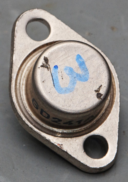
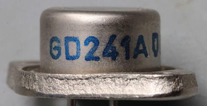
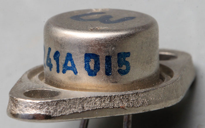
The GD241 is a germanium power transistor with a Vce of 35V (Rbe=50Ω). It can conduct up to 3A. The letter at the end of the designation, here an A, stands for the gain factor of the transistor (A: 18-35, B: 28-56, C: 45-90). The datasheet specifies the maximum junction temperature as 85°C. This is 10°C higher than the GD180 (https://www.richis-lab.de/BipolarA06.htm), which is probably one reason why the maximum power dissipation of 10W is twice as high. ft is at least 450kHz. The sign following the letter A is the logo of the "Röhrenwerk Neuhaus".


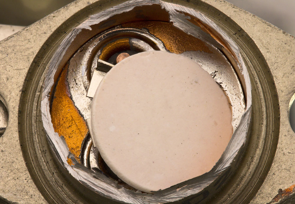
A large white plate was inserted into the housing to bind any moisture that may occur.


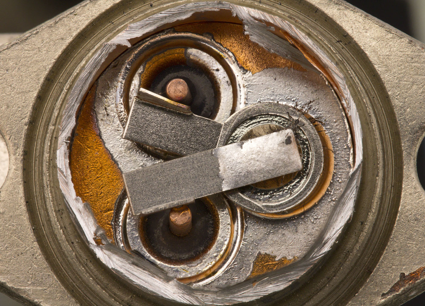
The construction of the transistor corresponds to the construction of the GD180. This is not surprising, since this GD180 was manufactured in the Röhrenwerk Neuhaus too.

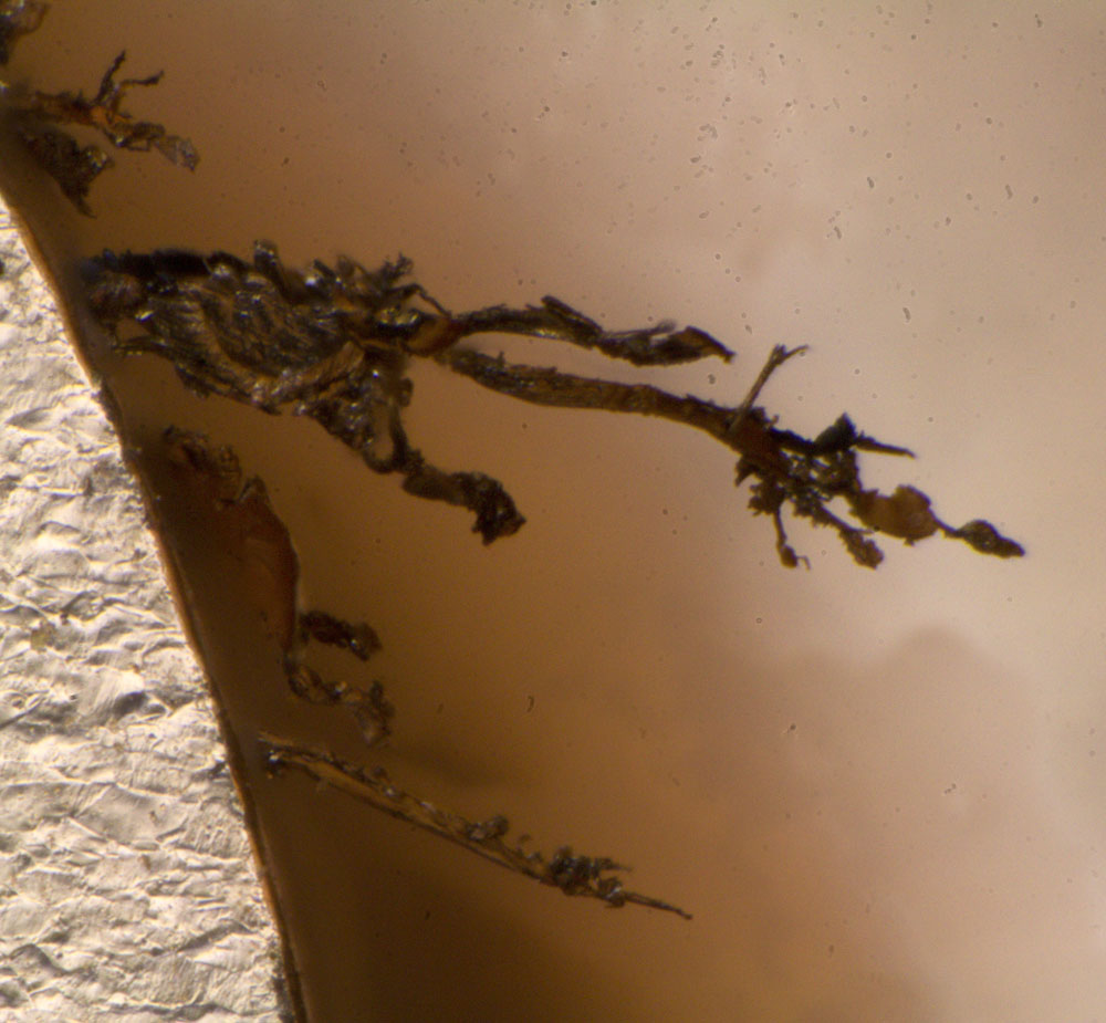
In the overview you can already see that dendrites were formed in this transistor. Similar dendrites were found in the Tesla GD609 (https://www.richis-lab.de/Bipolar65.htm). In the GD609, however, the inside of the case was heavily corroded, no traces of corrosion can be found here.


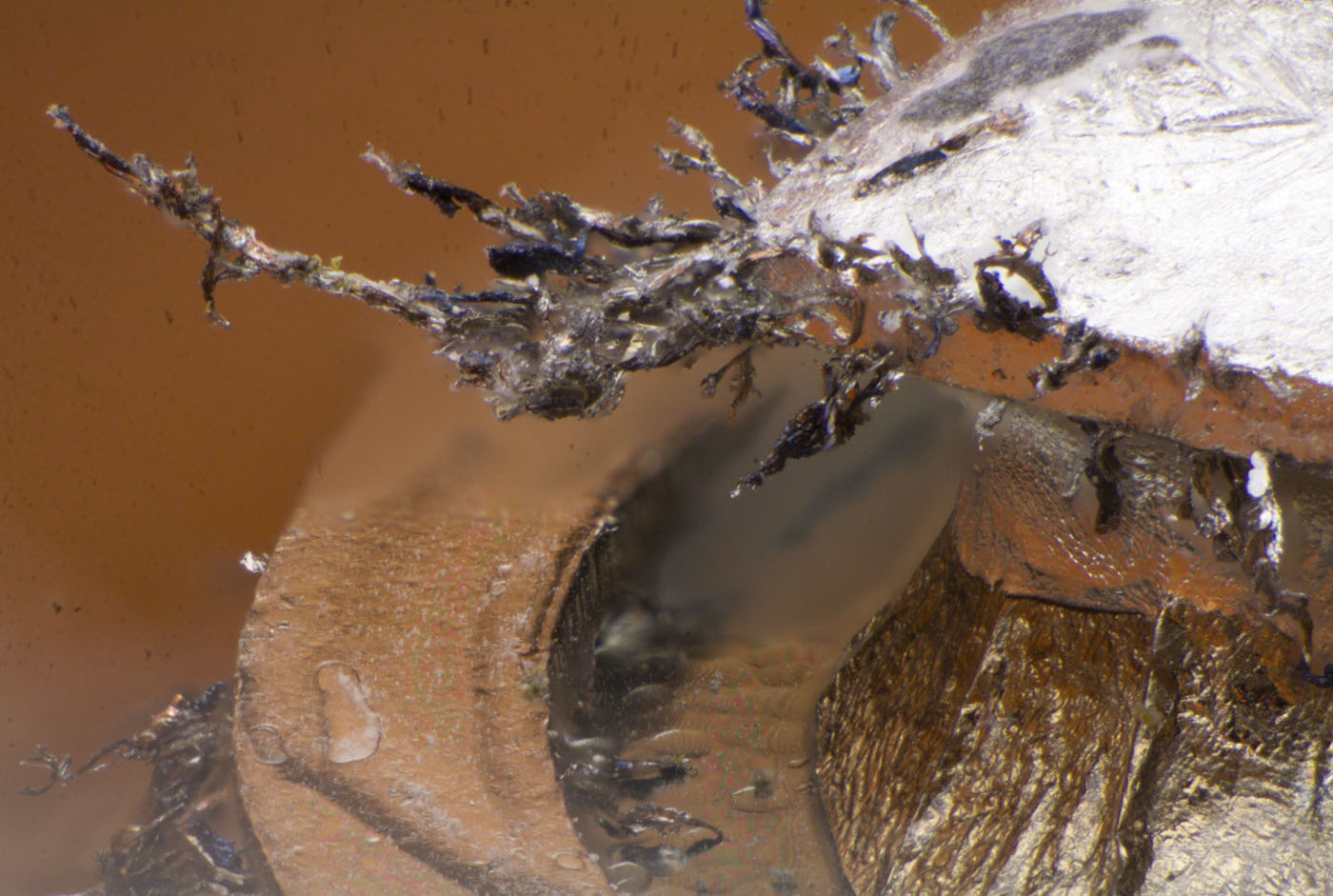
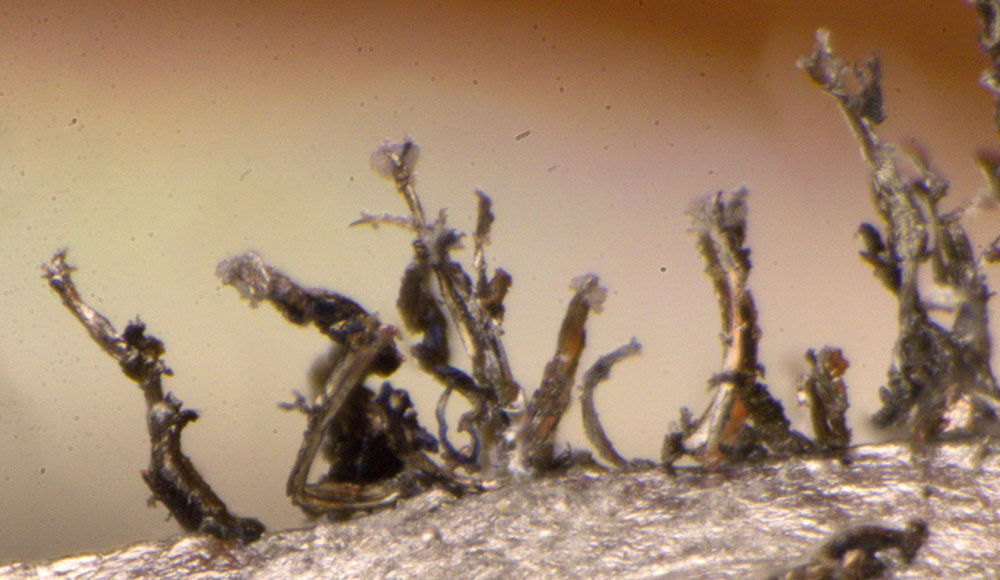
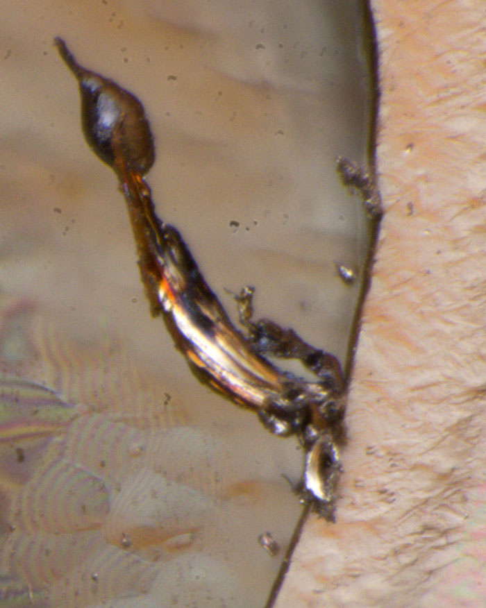
The dendrites are mainly located at the front edge of the element that contacts the emitter and around the base ring. Dendrites have also formed on the pin bushing. Smaller parts have broken off and are lying on the bottom of the housing.


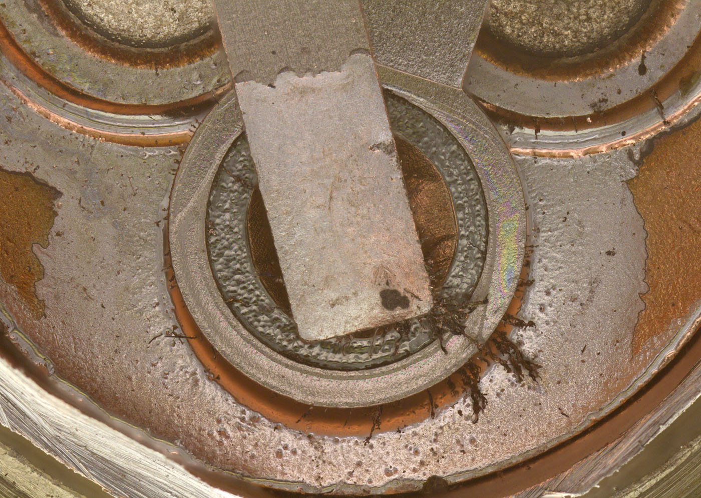
The finely branched dendrites are difficult to image photographically. Especially with several dendrites in different focus planes, focus stacking often does not provide an optimal image. Even with a lot of post-processing, some weaknesses remain. In this case, development into two different focus areas makes it somewhat easier to recognize the dendrites.


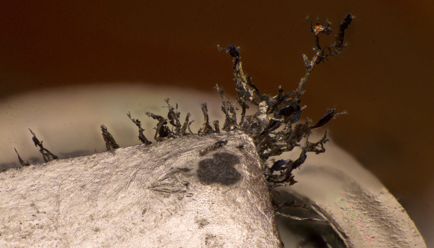
Most of the dendrites of the emitter junction originate from the upper edge and grow horizontally or slightly upwards. However, dendrites have also formed on the lower edge, approaching the base ring.


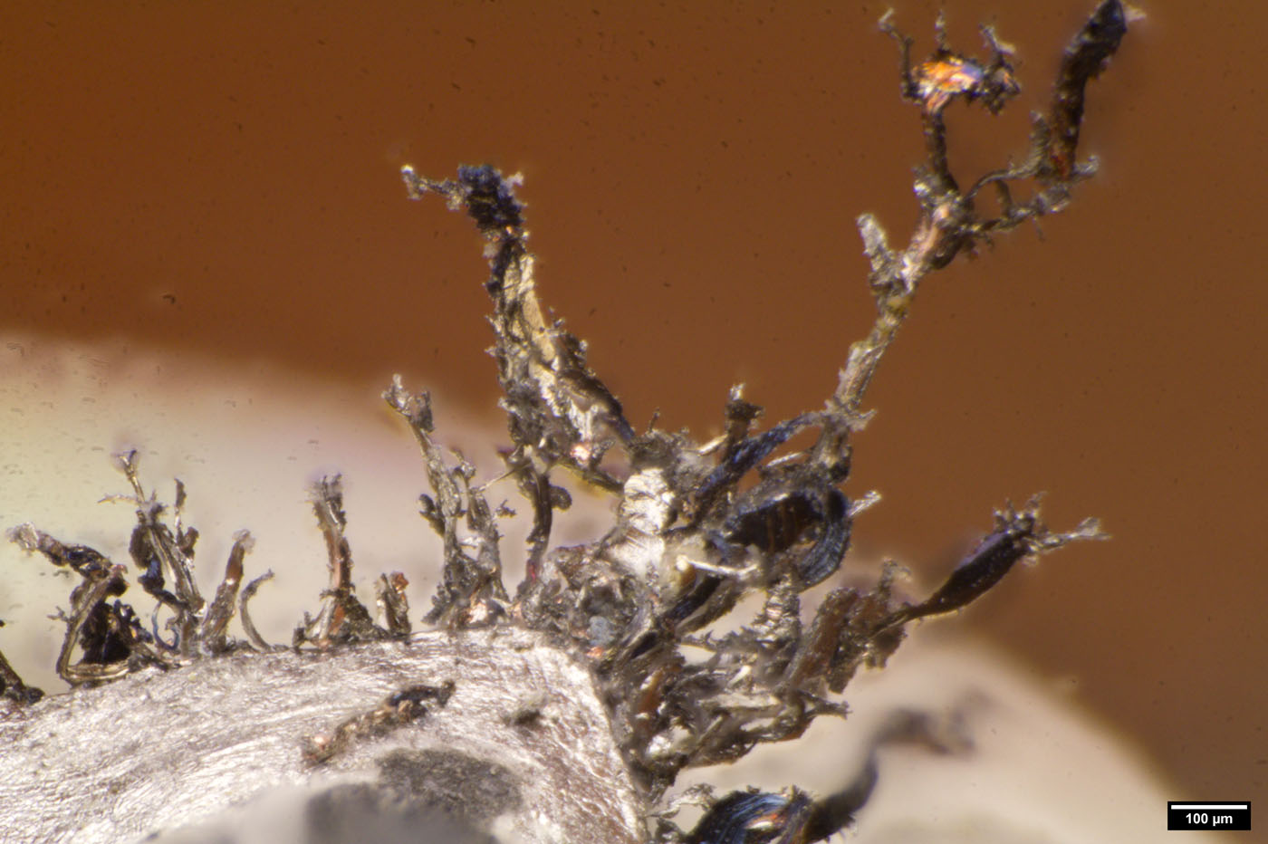
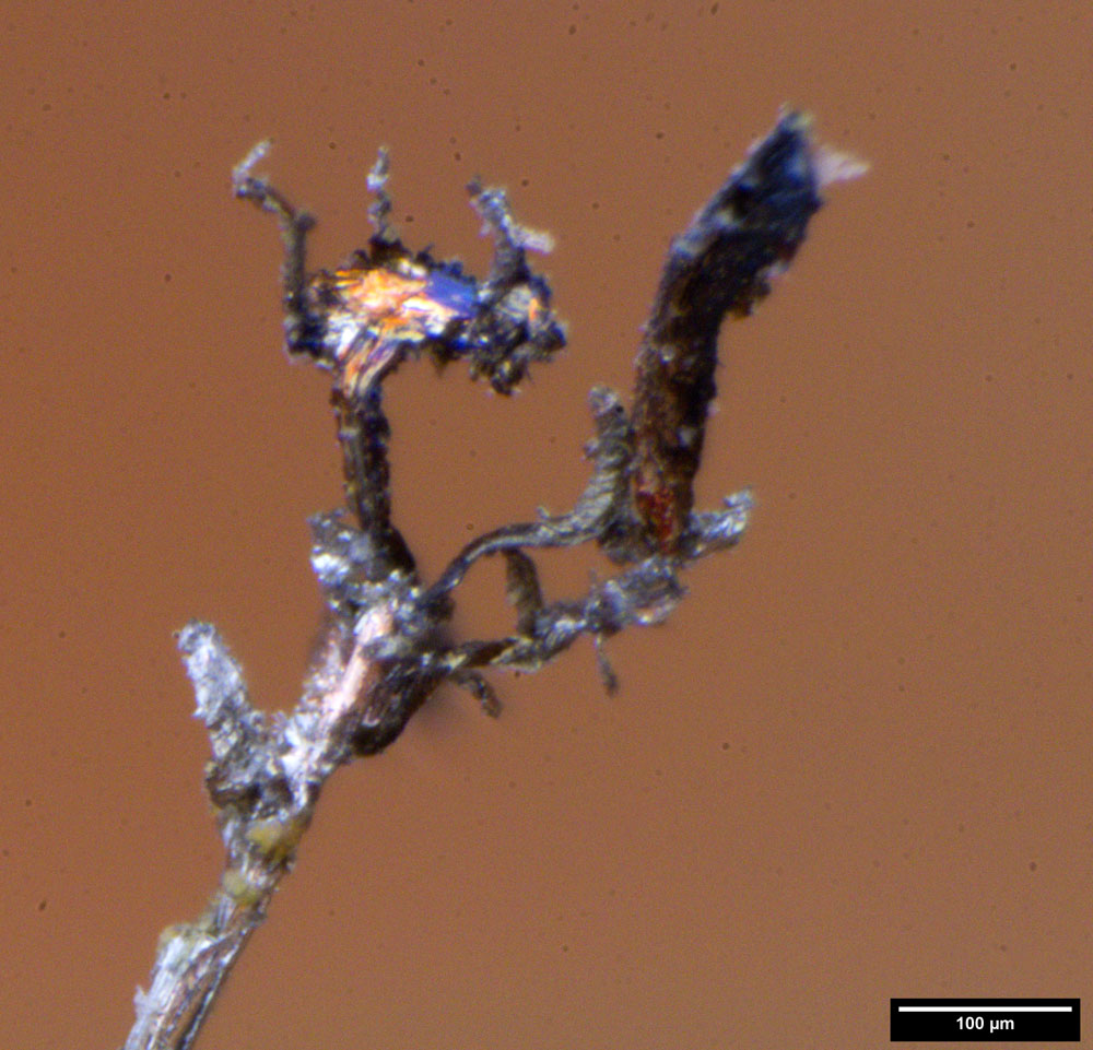
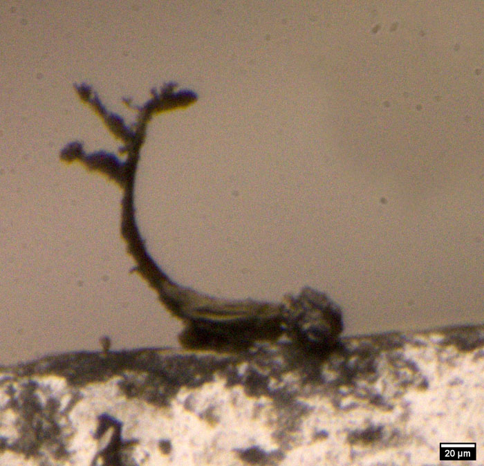
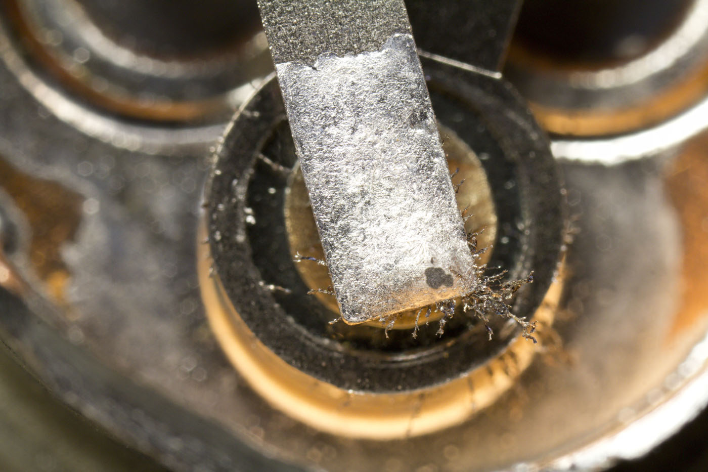
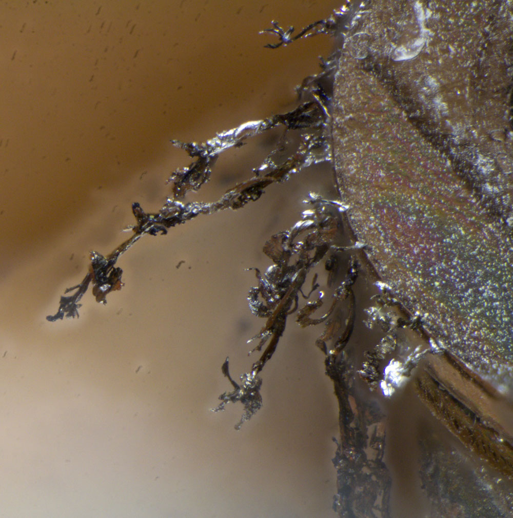
The larger dendrites sometimes form quite massive structures. At the ends, however, they always have very fine branching. It remains unclear which metals are in the dendrites.


In some cases, the tips of the uppermost dendrites carry remnants of the desiccant.


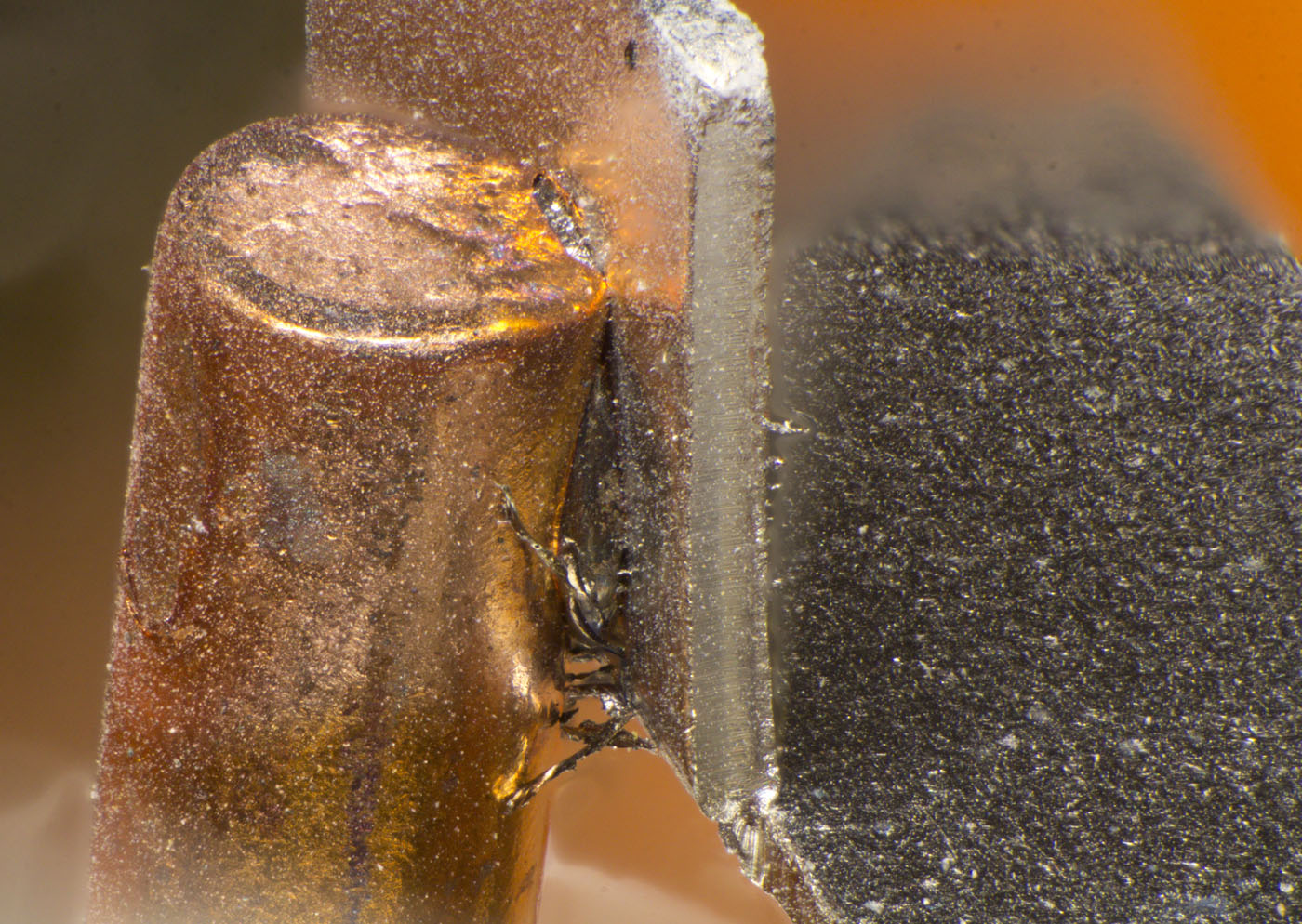
The dendrites are not only formed in areas covered with solder. Such crystals are also found between the pin and the emitter contact plate.


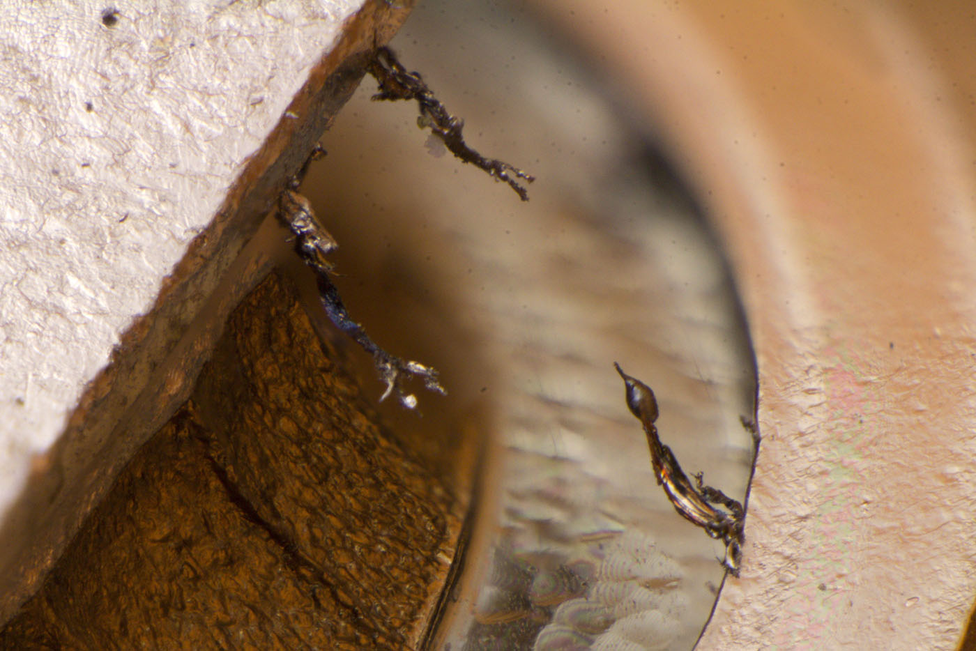
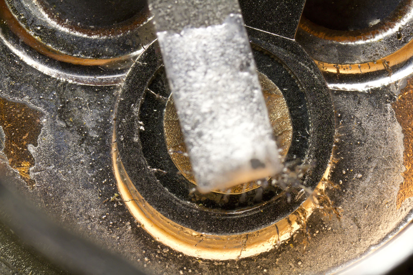
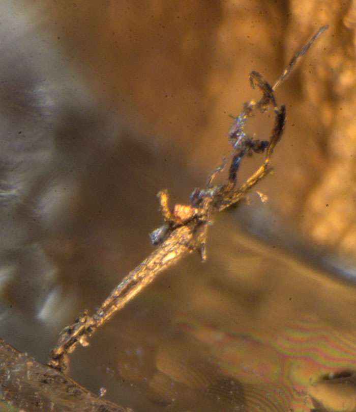
Dendrites have also formed on the base ring. One of those that grew in the direction of the emitter contact has an unusually round structure at the tip. It could be that a short circuit had already formed here, which then melted due to the current flow.


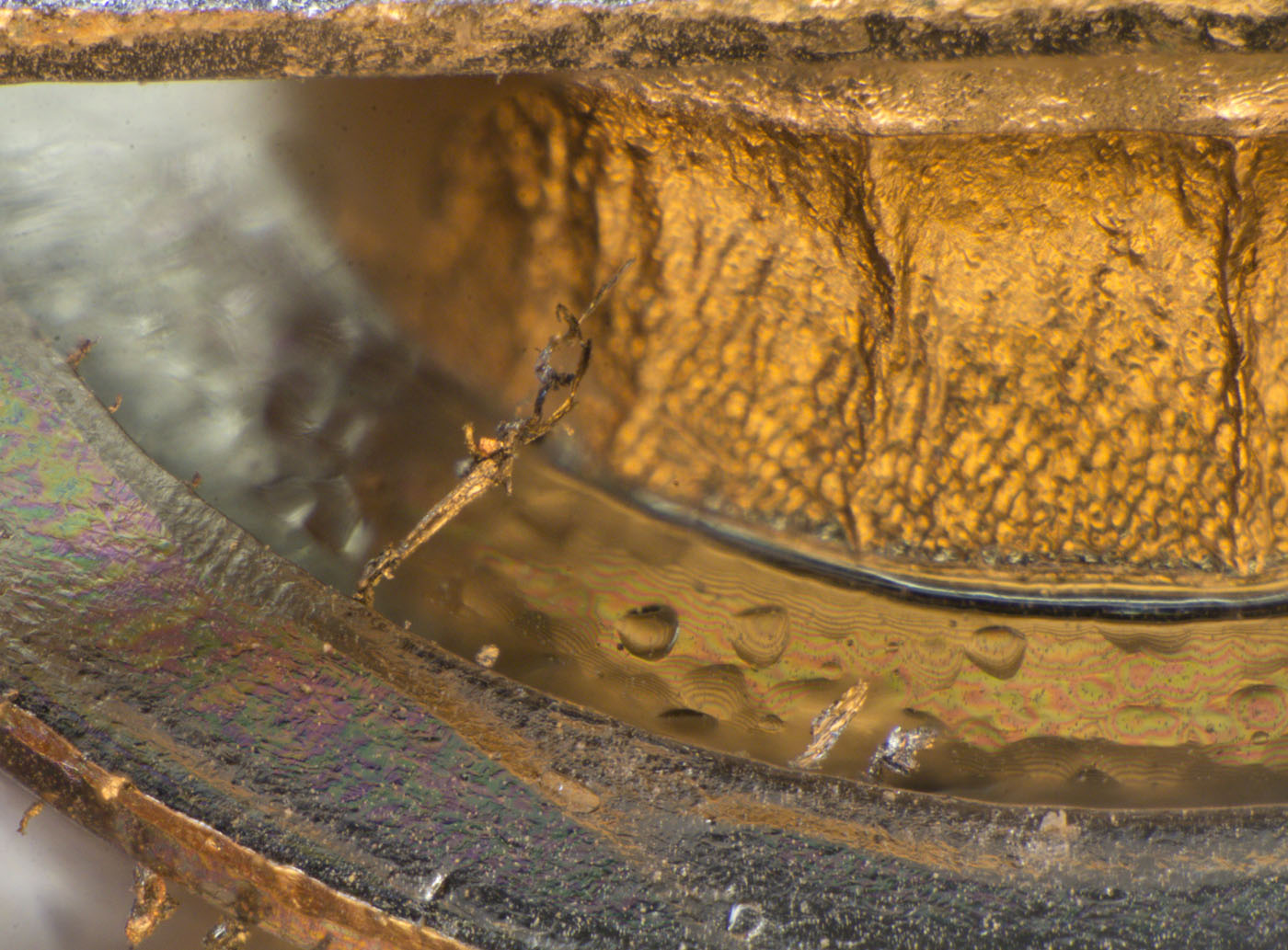
Another dendrite is already very close to the emitter contact.


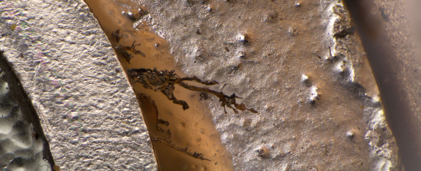
The majority of the dendrites on the base ring are directed toward the base plate of the transistor. Here, however, it may be that the drying tablet has bent the dendrites downward.


https://www.richis-lab.de/BipolarA12.htm

 :-/O
 
The following users thanked this post: SeanB, RoGeorge

Online NoopyTopic starter

  • Super Contributor
  • ***
  • Posts: 1735
  • Country: de
    • Richis-Lab
Re: Transistors - die pictures
« Reply #638 on: November 07, 2022, 04:51:34 am »


A long time ago I had a TPIC2404.


There are protection structures at the input but they are not easy to read and my first interpretation was probably wrong.

It seems there are two transistors. The one transistor is clearly visible (yellow). The potential of the bondpad is apparently conducted from the upper metal layer to the collector via the lower metal layer. The collector area appears purple. The buried collector shows up as a thin frame. The frame is somewhat displaced, which often occurs with low-lying layers. The collector potential is tapped at the top edge and routed to the rest of the TPIC2404 circuitry. Between the two collector contacts are one emitter and two base terminals. The emitter is connected directly to ground, while the base is connected to ground via a resistor.

The structure below the first transistor seems to represent a more unconventional transistor (cyan). While the upper transistor has a vertical structure, the lower transistor is a lateral transistor. The collector area, which is connected to the ground potential, can be seen directly. With the p-doped isolation frames and the adjacent n-doped collector areas of the first transistor, another NPN transistor is formed. The dopants and the shapes of this transistor are of course rather unusual.


You get the following circuit. Normally, both transistors should block the voltage. The transistor Q2 should serve as protection against negative voltages. It ensures that no uncontrolled current flows through the substrate. If there is a negative potential at the bondpad, the transistor will conduct current directly from the adjacent ground terminal.

Transistor Q1 serves as overvoltage protection. With a suitable design, this transistor breaks down before the rest of the circuit is damaged and diverts overvoltage pulses on a direct path to ground.


https://www.richis-lab.de/Bipolar30.htm

 :-/O
 
The following users thanked this post: SeanB, RoGeorge

Online NoopyTopic starter

  • Super Contributor
  • ***
  • Posts: 1735
  • Country: de
    • Richis-Lab
Re: Transistors - die pictures
« Reply #639 on: November 13, 2022, 07:56:38 am »


E1 => BFS17, a HF transistor with a ft of round about 2GHz. Vce is 25V and Ic is allowed to go up to 25mA. The low Veb of 2,5V shows how much dopand is in the silicon.


The die of the BFS17 is very small, measuring 0,32mm x 0,28mm.
It is really hard to clean...  ::)


The transistor has the typical structure where base and emitter contacts mesh on the base surface.


https://www.richis-lab.de/BipolarA13.htm

 :-/O
 
The following users thanked this post: SeanB, SilverSolder, Miyuki

Online NoopyTopic starter

  • Super Contributor
  • ***
  • Posts: 1735
  • Country: de
    • Richis-Lab
Re: Transistors - die pictures
« Reply #640 on: November 26, 2022, 04:27:20 am »
The die of a 2N3439 transistor in visible light, as well as photos showing the light emissions under Emitter-Base breakdown, and the IR light emitted when the base junction is forward biased. On a CMOS sensor with the IR filter removed there is just enough IR sensitivity to see the IR light emitted by PN junctions in forward bias. 

Weston did the first IR pictures in this thread.
I had planned to do some IR pictures too. Now here they are.
For the a first try I took a bulky BUX22 but I will do more complex (and interesting?) parts too.


This BUX22 from 1987 is still labeled with the Thomson Semiconducteurs logo. My BUX22 from 1988, on the other hand, already bears the logo of ST Microelectronics: https://www.richis-lab.de/Bipolar07.htm


Like the BUX22 from 1988, the base plate of the case is very thick. It thus represents a quite efficient heatspreader.


The pins are very thick, which makes absolute sense for currents up to 50A.


It turns out that this BUX22 is built the same way like the BUX22 from 1988.


No differences can be seen in the details either.


[end of part 1]

 
The following users thanked this post: SeanB, RoGeorge

Online NoopyTopic starter

  • Super Contributor
  • ***
  • Posts: 1735
  • Country: de
    • Richis-Lab
Re: Transistors - die pictures
« Reply #641 on: November 26, 2022, 04:28:35 am »
[part 2]


First some BE breakdown (-13V, 0,01A). Unlike the BUX22 from 1988 (https://www.richis-lab.de/Bipolar07.htm), the two transistors in this BUX22 behave significantly differently.


Even with a current of 0,1A the left transistor still remains almost completely dark.


At a current of 0,5A a relevant current flow also starts in the left transistor.


Up to a current of 1A the differences are still clearly visible. While with asymmetrical light effects on one die one can assume an inhomogeneous structure, the different light appearance on the two dies does not necessarily tell something about the current distribution in normal operation.


[end of part 2]

 
The following users thanked this post: SeanB, RoGeorge, mawyatt

Online NoopyTopic starter

  • Super Contributor
  • ***
  • Posts: 1735
  • Country: de
    • Richis-Lab
Re: Transistors - die pictures
« Reply #642 on: November 26, 2022, 04:29:47 am »
[part 3]


If a current flows across a pn junction, charges recombine there. During recombination, partially photons are emitted. Light emitting diodes are based on this effect. In light emitting diodes, so called direct semiconductors are used, in which it is very likely that recombination is associated with the emission of a photon.

In contrast, silicon is an indirect semiconductor. If charges recombine with light radiation, they must emit a phonon as well as a photon. Phonons are lattice vibrations which ultimately increase the temperature of the semiconductor. At the same time, this means that recombination is much less likely and the energy remaining for the emitted photons is reduced by the energy of the phonons. A large fraction of the charges recombine nonradiatively, passing energy to other electrons as part of the Auger effect, which ultimately heats the semiconductor.

The small bandgap of silicon and indirect recombination mean that just relatively long-wavelength radiation is produced in the pn interface. This infrared radiation is not readily visible. Normal SLR cameras have infrared filters in front of the sensor. If this filter is removed, the infrared radiation can be made visible. However, the camera and its optics are not optimized for such long wavelengths, which means that the exposure metering no longer works perfectly and the image quality is not optimal in every case.

Here, a current of 1A flows across the base-emitter path of the BUX22. The Canon EF 100mm f/2.8L Macro lens was used in its normal configuration. With an aperture of 2.8 and ISO 1600, nevertheless an exposure time of 2s is necessary to make the relatively dark purple glow visible. A closer look already shows that the glow is somewhat blurred compared to the rest of the image and radiates beyond the spaces between the metal.


If you set a CE current of 5A and hold the BE current at 1A, the luminous effect will be slightly brighter.


With a CE current of 10A the light intensity is already significantly higher.


With 15A a certain concentration of the luminance into the center of the transistors occurs. Here the over-radiation into the metal layer is clearly visible.


The following images were taken with the Canon EF-S 10-22mm f/3.5-4.5 lens in retro position. This configuration shows significantly less outshining.

At an ISO of 3200 and an exposure time of 3,2s the glow of a BE current of 0,5A is just visible.


If the CE current is increased to 5A, the glow becomes brighter, especially at the long edges of the emitter contacts. At the outer edges and in the center, the interfaces are somewhat darker.


With a current of 10A through the collector the light color seems to shift slightly to reddish. The light intensity increases and the inner areas also become brighter.


If the collector current is increased to 15A, the concentration of the luminance on the inside of the transistor also becomes apparent here.


https://www.richis-lab.de/BipolarA14.htm

 :-/O 8)
 
The following users thanked this post: SeanB, RoGeorge

Offline RoGeorge

  • Super Contributor
  • ***
  • Posts: 6204
  • Country: ro
Re: Transistors - die pictures
« Reply #643 on: November 26, 2022, 09:22:32 am »
The junction starts to emit visible light in localized dots of light at first, but in infra red the light seems to be uniformly spread, just dimmer at lower currents.  Why no dots seen in IR?

Online NoopyTopic starter

  • Super Contributor
  • ***
  • Posts: 1735
  • Country: de
    • Richis-Lab
Re: Transistors - die pictures
« Reply #644 on: November 26, 2022, 09:29:51 am »
The visible light comes in reverse breakdown. It's an avalanche effect. Like in zener diodes that's a local effect. There is a weakest point breaking down and the next one comes as soon as the current through the first one is high enough to rise the voltage above the breakdown voltage of the next area.

The IR comes in normal conduction mode. The manufacturer do everything to get that current (and light) as uniform as possible. Otherwise you get problems with hot spots. Distributed emitter resistance helps for example.
 
The following users thanked this post: SeanB, RoGeorge, karpouzi9

Online NoopyTopic starter

  • Super Contributor
  • ***
  • Posts: 1735
  • Country: de
    • Richis-Lab
Re: Transistors - die pictures
« Reply #645 on: December 02, 2022, 07:23:38 pm »
Some more IR light!  8)

Do you remember the SF137 built by the Halbleiterwerk Frankfurt Oder:


A small "HF" transistor with a common design.


As described with the Thomson Semiconducteurs BUX22, an infrared image can be used to visualize where charges recombine.

In the above images, Ibe is 30mA while Ice increases from 0A to 0,1A to 0,2A. Without collector current, most of the light occurs in the base region. On closer inspection, one can guess that the emitter region is less bright. As Ice increases, the light shifts toward the emitter, while the base region becomes darker.


The picture above is taken from the IEEE publication "Multi-dimensional current flow in silicon power transistors operating in the saturation mode" by R. A. Sunshine and has been recolored here. The document explains the background of the different light phenomena. It is important to understand that in a normal bipolar transistor there is a parasitic diode next to the transistor itself. It is formed between base and collector.

One might think that a base-emitter current would choose the shortest path from the base to the emitter. However, as long as there is not too much collector current flowing, the dominant current path is completely different. The special structure of a bipolar transistor with its very thin base layer ensures that most of the electrons (cyan) leaving the emitter pass through the base region and arrive in the collector. For the positive charges (purple), the path to the collector is in most cases more attractive than the path to the emitter. Consequently, the base current first flows into the collector and from there to the emitter.

Apart from isolated recombination effects under the emitter, most of the recombination takes place under the base terminal, where the corresponding light effect occurs.


This image is taken from the IEEE publication too (and was recolored). It shows the charge movements with increasing collector current. The more electrons flow from emitter to collector and leave the transistor there, the fewer electrons flow from the collector back to the base terminal. The positive charge carriers of the base flow into the base area under the emitter, where they provide the necessary drive of the transistor. Recombination and the associated luminous effect shift accordingly to the emitter area.


A comparison at different Ibe and Ice is difficult, because the light intensity is very low and the camera system does not work very efficiently in the infrared range. However, certain tendencies can be seen quite well.

As long as no Ice is flowing, the luminance in the base area increases with increasing Ibe. The luminous area seems to increase a little. The emitter area always remains slightly darker. With increasing Ice, the luminous effect is concentrated in the emitter area and the base area becomes darker. At high Ibe the base area never becomes completely dark.

The combination of a small Ibe with a very large Ice stands out, because there the emitter region is much brighter than at the medium base currents. Here the transistor is operated in saturation. This ensures maximum concentration of the recombination region. Not only does the recombination take place completely in the emitter area, it is also limited to the edge of the emitter area, which further increases the luminance there.


https://www.richis-lab.de/Bipolar75.htm#IR

 :-/O
 
The following users thanked this post: SeanB, T3sl4co1l, SilverSolder, RoGeorge, Miyuki, razvan784, magic, DavidKo, Weston, mawyatt

Offline SilverSolder

  • Super Contributor
  • ***
  • Posts: 6126
  • Country: 00
Re: Transistors - die pictures
« Reply #646 on: December 04, 2022, 01:22:58 pm »
Very interesting stuff.  So does this mean that effectively, the 'resistance' in a semiconductor 'happens' at the junction - and that's why it gets hot there?  I.e. there is no way around Ohm's law, even for a semiconductor (there is equivalent "resistance" at the junction, and putting a current through it will make it hot).
 

Online T3sl4co1l

  • Super Contributor
  • ***
  • Posts: 21693
  • Country: us
  • Expert, Analog Electronics, PCB Layout, EMC
    • Seven Transistor Labs
Re: Transistors - die pictures
« Reply #647 on: December 04, 2022, 02:28:13 pm »
Sort of.  Resistive loss is non emissive.  Remember this is near IR, not far (thermal).  We're seeing recombination here -- weakly because silicon is indirect bandgap, but still something.

It's also not where heat is generated, because the C-B junction isn't glowing when it's reverse biased (Vce > Vce(sat))!

This is just showing where the diode-like current flows.  And it's fairly remarkable to see the base current flow into the collector to the emitter.

..I mean, in saturation, it is where heat is generated, but still not quite in proportion because the emitter is generally brighter but most of the dissipation is still in the collector.

Hope that clears things up :)

Tim
Seven Transistor Labs, LLC
Electronic design, from concept to prototype.
Bringing a project to life?  Send me a message!
 
The following users thanked this post: SilverSolder

Online NoopyTopic starter

  • Super Contributor
  • ***
  • Posts: 1735
  • Country: de
    • Richis-Lab
Re: Transistors - die pictures
« Reply #648 on: December 04, 2022, 02:30:18 pm »
Very interesting stuff.  So does this mean that effectively, the 'resistance' in a semiconductor 'happens' at the junction - and that's why it gets hot there?  I.e. there is no way around Ohm's law, even for a semiconductor (there is equivalent "resistance" at the junction, and putting a current through it will make it hot).

Your point is that the IR at the junction generates most of the losses?
I'm pretty sure the IR is just a small part of the power dissipation. Silicon is a very inefficient light source. Most recombinants don't dissipate a photon. I need ISO 32.000 and 4 seconds and more than 10mA before I see any light.
One important point to get low losses is a low collector resistance. That is why today you have a n++ collector contact and a likewise thin n collector.

Edit: And everything Tim said.  ;D
« Last Edit: December 04, 2022, 09:19:03 pm by Noopy »
 
The following users thanked this post: SilverSolder

Offline SilverSolder

  • Super Contributor
  • ***
  • Posts: 6126
  • Country: 00
Re: Transistors - die pictures
« Reply #649 on: December 04, 2022, 09:15:13 pm »

I see, thank you both,  I wasn't appreciating that the IR radiation seen is not actually caused by heat but instead is a side effect of recombination.  That is rather amazing, actually -  seeing electrons at work, almost!


Share me

Digg  Facebook  SlashDot  Delicious  Technorati  Twitter  Google  Yahoo
Smf