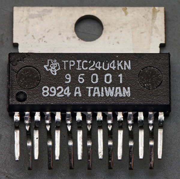
TPIC2404: four 1A-Smart-Transistors with overvoltage protection, overcurrent protection, freewheeling diodes to an external potential, enable input and error output.
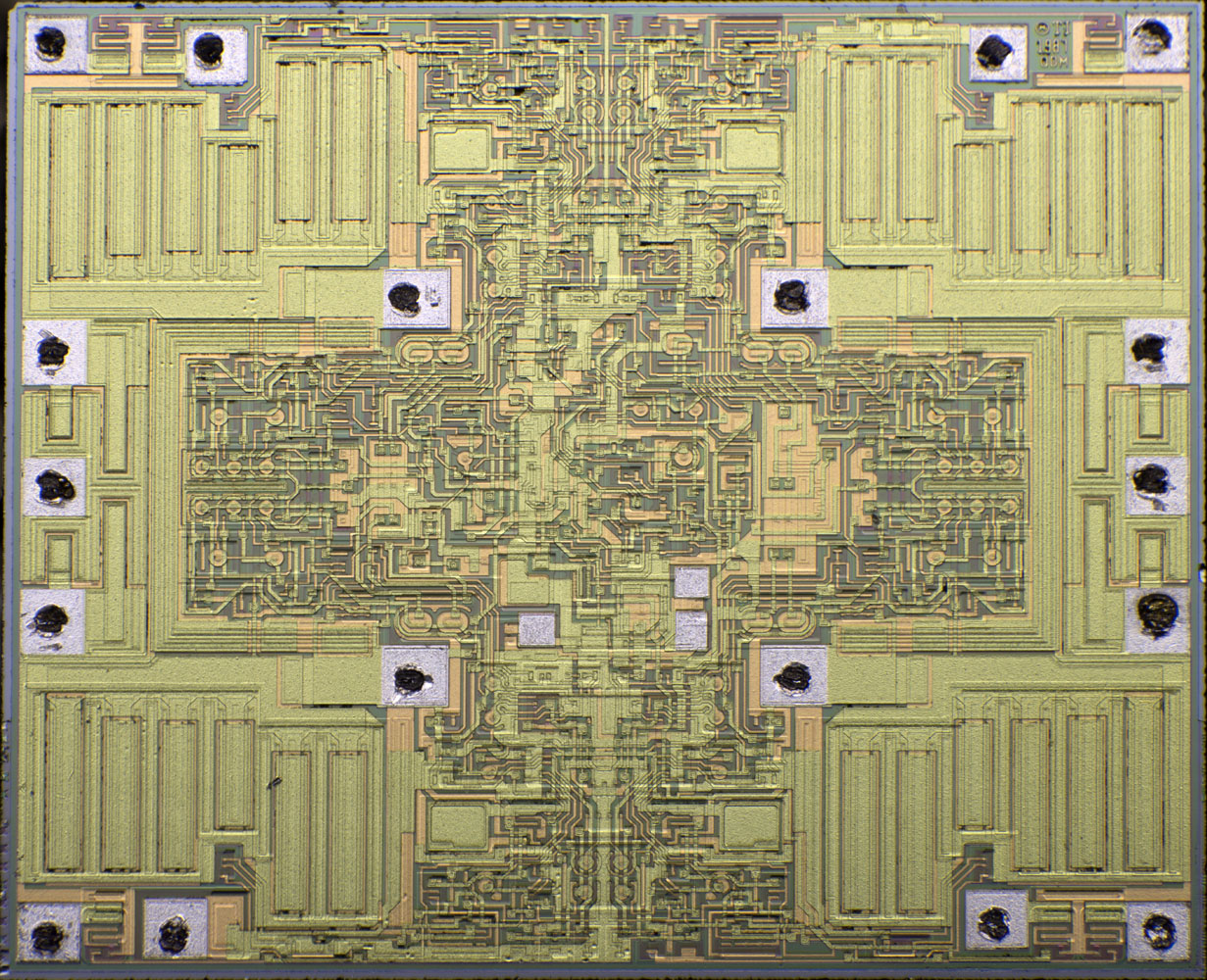
The die is 3,9mm x 3,4mm and uses two metal layers.
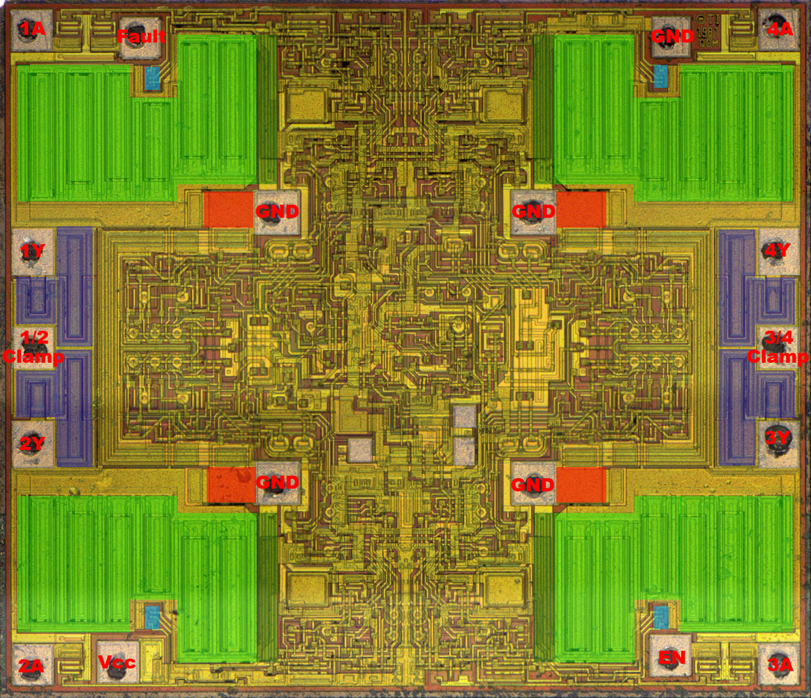
You can identify a lot of parts of the TPIC2404:
Green: Output transistor
Dark green: Output transistor driver
Dark blue: Freewheeling / Clamping diodes.
Red: Shunt for overcurrent protection
Blue: Overtemperature protection
1987
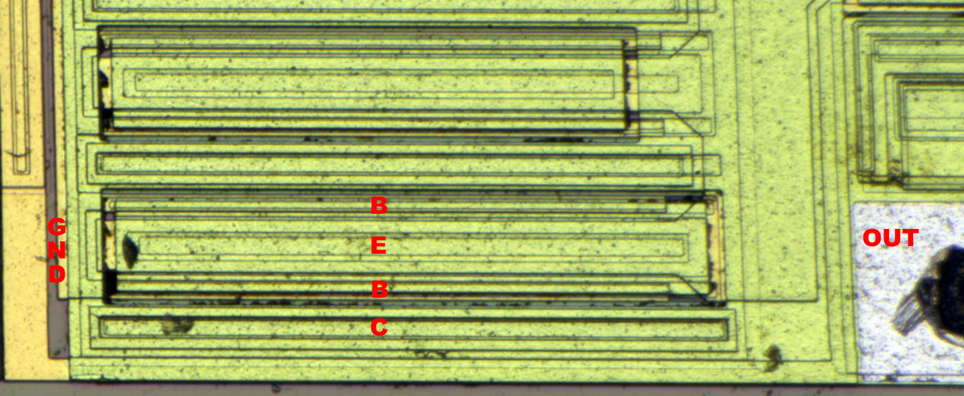
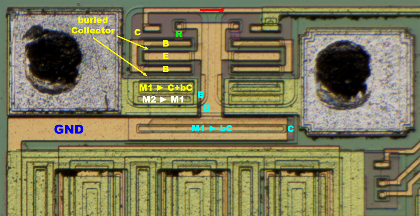
The parts of the output transistor are hard to identify because of the two metal layers.
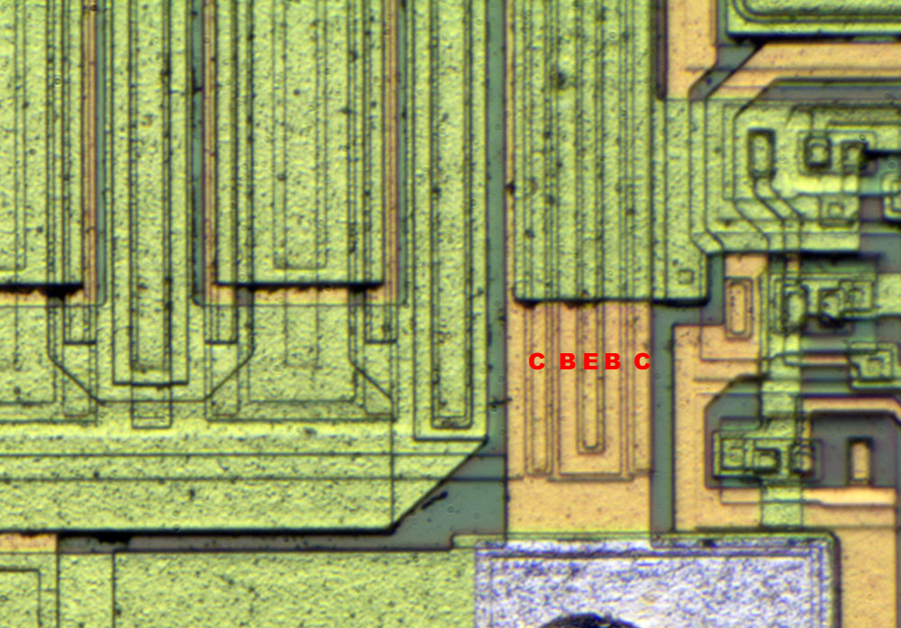
Same with the driver transistor.
Shunt-Current-Measurement
Temperature sensor
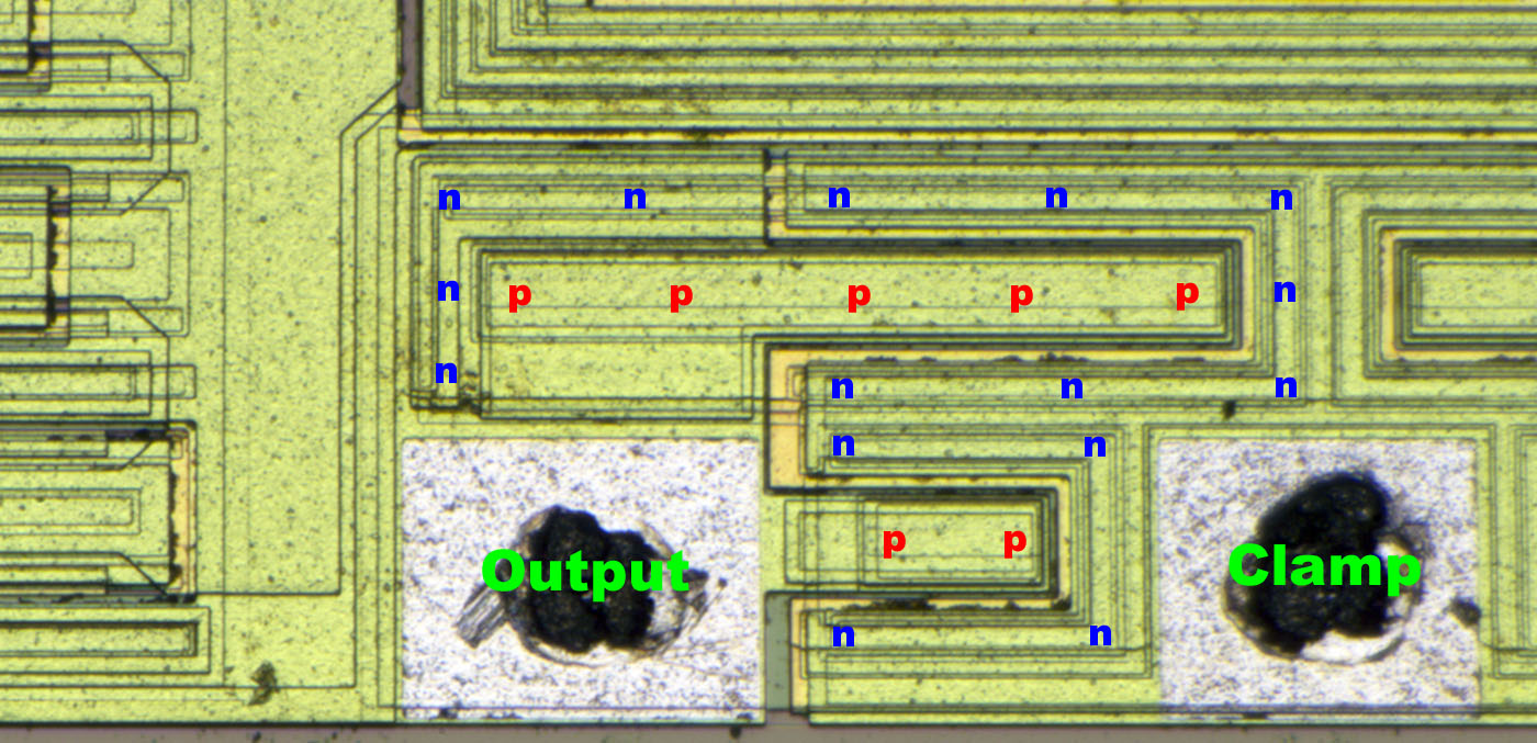
Freewheeling / Clamping diode
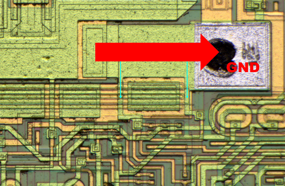
It uses the two metal layers in parallel to get a low resistance in this small area.
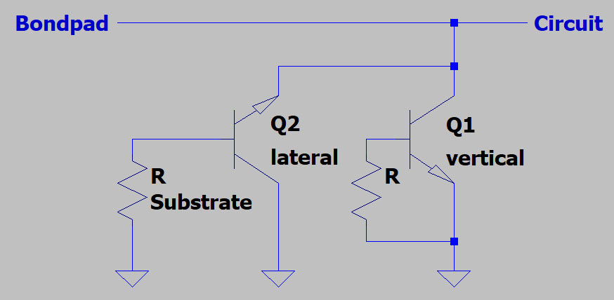
The input protection has a transistor at the bondpad with base and emitter connected (red). Base-collector gives you a diode with a high breakdown voltages and protects the circuit against negative voltages.
In the collector area there is a MOSFET which can switch to ground (black). The green resistor is a pull-down for the gate. Via a small capacitor (yellow) a voltage surge activates the MOSFET and is shunted to ground.
 https://www.richis-lab.de/Bipolar30.htm


