Author Topic: Transistors - die pictures  (Read 188415 times)

Phoenix, antenna and 3 Guests are viewing this topic.

Offline NoopyTopic starter

  • Super Contributor
  • ***
  • Posts: 1730
  • Country: de
    • Richis-Lab
Re: Transistors - die pictures
« Reply #575 on: April 05, 2022, 07:36:09 pm »


Who knows TET (Tallinna Elektrotehnika Tehas)? It´s an Estonian semiconductor manufacturer. TET Estel still produces semiconductors and power electronic devices.

Here we have a power thyristor built by TET, a T62-160-10.


The name of the device is written onto the package by hand.


In the "Applikative Informationen" of the VEB Applikationszentrum Elektronik Berlin 2/1984 you can find a explanation for the naming.

T stands for a thyristor, sometimes you have a second letter for special types.
62 is the thyristor familiy.
160 stands for 160A
10 stands for a blocking voltage of 1000V
The other numbers are probably dynamic parameter like the critical voltage slew rate.


The ground plate is 65mm in diameter and has a height of 7mm. The cylinder wall is 3mm thick.


A green glass like material closes the package around the cathode contact.


The base plate is made of copper.


The thyristor itself is 3cm in diameter and protected with a red coating.

The cathode wire is crimped in a short wire-end sleeve that is soldered onto the thyristor die.


The thyristor die is placed on a disc that is soldered to the package.


The cathode contact is quite high, probably to get it mechanical stable.


At some places around the cathode contact there are dark areas that possibly contain the cathode doping.  :-//

There is a solder ring around the cathode, perhaps to distribute the gate potential? Interestingly the solder ring doesn´t connect to the gate contact.


It looks like the die was processed two times to flatten it to the edge. You can see typical etch structures.


https://www.richis-lab.de/Bipolar99.htm

 :-/O
 
The following users thanked this post: SeanB, doktor pyta, SilverSolder, RoGeorge, ch_scr, mawyatt

Offline NoopyTopic starter

  • Super Contributor
  • ***
  • Posts: 1730
  • Country: de
    • Richis-Lab
Re: Transistors - die pictures
« Reply #576 on: April 06, 2022, 03:28:12 am »
It looks like the name of the thyristor is TB2-160-10.
If you compare the "first 6" with the second 6 the first one is more edged like a cyrillian B.
B then stands for a  fast transistor.

I thought is could be a T62 because you still can buy T62 thyristors but you don´t find much information about TB2 thyristors.

I have changed the article.  :-/O

Offline MegaVolt

  • Frequent Contributor
  • **
  • Posts: 917
  • Country: by
Re: Transistors - die pictures
« Reply #577 on: April 07, 2022, 08:07:49 am »
Yes, it looks like ТБ2-160
Here is the information:
https://eandc.ru/catalog/detail.php?ID=15835
 

Offline NoopyTopic starter

  • Super Contributor
  • ***
  • Posts: 1730
  • Country: de
    • Richis-Lab
Re: Transistors - die pictures
« Reply #578 on: April 07, 2022, 10:59:26 am »
Yeah, that looks like a brother!  :-+

Thanks!

Offline NoopyTopic starter

  • Super Contributor
  • ***
  • Posts: 1730
  • Country: de
    • Richis-Lab
Re: Transistors - die pictures
« Reply #579 on: April 11, 2022, 08:55:10 am »


One more Tesla power transistor. The KD617 is the complementary PNP to the KD607. The specs are the same: It can isolate 80V, conduct 10A and ft is 2MHz.


On the backside you can see the circle of the copper cylinder in the base plate that conducts the heat very efficient.


We have seen the red potting a lot in the Tesla transistors.


The edge length of the die is 4,5mm. That´s the same size as the KD616 (https://www.richis-lab.de/Bipolar87.htm). The KD615, the KD616 and the KD617 are probably the same transistors just binned with respect to their voltage rating.


Here you can see the base emitter junction. The edges around the metal structures are the edges of the contact vias.


The MESA structure is surprisingly unsteady. At the edge of the transistor there are quite deep and unsteady pits. It looks like the etching process didn´t work too well.


https://www.richis-lab.de/BipolarA01.htm

 :-/O
 
The following users thanked this post: SeanB, SilverSolder, RoGeorge, capt bullshot

Offline NoopyTopic starter

  • Super Contributor
  • ***
  • Posts: 1730
  • Country: de
    • Richis-Lab
Re: Transistors - die pictures
« Reply #580 on: April 22, 2022, 07:24:27 pm »

Offline NoopyTopic starter

  • Super Contributor
  • ***
  • Posts: 1730
  • Country: de
    • Richis-Lab
Re: Transistors - die pictures
« Reply #581 on: April 23, 2022, 08:52:19 pm »


The SF123 (TO-5) is a transistor built by the Halbleiterwerk Frankfurt Oder. DO stands for a production in April 1974. The maximum collector emitter voltage is 40V. The SF122 and the SF121 appear to be poorer grades. They offer the same specifications, but Vce is just 30V and 20V. The SF123 allows 100mA continuously and up to 600mW.

The datasheet recommends the SF123 for LF and RF applications. However, the cutoff frequency is not excessive with typically 130MHz, minimum 60MHz. The SF137 (https://www.richis-lab.de/Bipolar75.htm) with its cutoff frequency of at least 300MHz is more suitable for high frequency applications.

As with the SF137 the current gain spread was initially very high. Values between 18 and 1120 were allowed. The transistors were binned in six groups. The SF123D offers a current gain of 112 to 280. This fits with the fact that from 1970 on just D and E types were produced.

The SF123 is a simple planar transistor. You can see that looking at the collector emitter saturation voltage. The transistor is manufactured on a n-doped substrate that forms the collector. In this substrate you dope base and emitter areas. The datasheet specifies a maximum Vcesat of 1V. The SF137 on the other hand is a planar epitaxial transistor. The substrate is heavily n-doped, which guarantees a low collector resistance. However, the collector region itself must not be doped too intense, otherwise the blocking voltage will be very low. For this reason, a thin, less heavily doped collector region is epitaxially deposited on the highly doped substrate. The result is a maximum saturation voltage of just 0.3V.


With an edge length of 1mm the die is twice as big as the SF137.


And some light...  8)
-8V 10mA


20mA


50mA


80mA


400mA


https://www.richis-lab.de/BipolarA02.htm

 :-/O
 
The following users thanked this post: SeanB, exe, RoGeorge, bsw_m, ch_scr, mawyatt

Online mawyatt

  • Super Contributor
  • ***
  • Posts: 3240
  • Country: us
Re: Transistors - die pictures
« Reply #582 on: April 24, 2022, 03:10:35 pm »
This looks like an old 2N706 transistor that wayback was somewhat famous for the avalanche mode relaxation oscillator behavior.

As always, nice image, and amazed at how many of these you produce :-+

Best,
Curiosity killed the cat, also depleted my wallet!
~Wyatt Labs by Mike~
 
The following users thanked this post: Noopy

Offline NoopyTopic starter

  • Super Contributor
  • ***
  • Posts: 1730
  • Country: de
    • Richis-Lab
Re: Transistors - die pictures
« Reply #583 on: April 26, 2022, 07:51:29 pm »
As always, nice image, and amazed at how many of these you produce :-+

Thanks! I do my very best to reduce the stockpile of interesting parts.  ;D


BD1428 - can anybody tell me who manufactured this dual transistor?

There is a notice written by myself stating that the BD1428 was built by the russian manufacturer Istok. Unfortunately I wasn´t able to find any proof for this statement and I found no hint were I got this information from.  :-//

It looks like the BD1428 has been manufactured in 1969.


The die is 0,55mm x 0,43mm and it is surprisingly dirty.

The two transistors are isolated with a structure formed like an eight. Like in the К1HT291Б (https://www.richis-lab.de/Bipolar71.htm) you can see no buried collector contact. Instead of this buried collector contact the metal contact is designed around half of the transistor.


https://www.richis-lab.de/BipolarA03.htm

 :-/O
 
The following users thanked this post: SeanB, RoGeorge

Offline jpe

  • Newbie
  • Posts: 2
  • Country: gb
Re: Transistors - die pictures
« Reply #584 on: April 29, 2022, 02:33:05 am »
I would like to see what a Zetex "super e-line" transistor looks like.  Other manufacturers now make them as low saturation voltage and high current gain parts.

Had a spare ZTX851, unfortunately the die cracked while decapping but most of it is still intact.

Die is aprox 1780x1780µm and has a perforated emitter design - layout looks very similar to the 2STD1665.


The following users thanked this post: SeanB, doktor pyta, exe, RoGeorge, Miyuki, ch_scr

Offline David Hess

  • Super Contributor
  • ***
  • Posts: 16607
  • Country: us
  • DavidH
Re: Transistors - die pictures
« Reply #585 on: April 29, 2022, 11:26:30 pm »
I would like to see what a Zetex "super e-line" transistor looks like.  Other manufacturers now make them as low saturation voltage and high current gain parts.

Had a spare ZTX851, unfortunately the die cracked while decapping but most of it is still intact.

Die is aprox 1780x1780µm and has a perforated emitter design - layout looks very similar to the 2STD1665.

So it is "just" a perforated emitter design.  I thought there must be more to it, and maybe there is.  The story I remember is that Zetex bought old IC fabrication equipment which supported a much finer feature size than the equipment normally used for discrete transistor production.  It looks like what they did is take the perforated or ring emitter design and scale it down to smaller transistors.  For a short time Zetex made a larger TO-225 or TO-220 part but I never got any.

Was a die shot of the D44/D45 series TO-220 ring emitter transistors posted?  A comparison to get an idea of the difference in feature size could be informative.

While not advertised as such and as might be expected from their construction, these Zetex transistors apparently have very low base spreading resistance leading to low noise.  Monolithic transistors built in an IC process like the LM394 and MAT series also have low base spreading resistance for low noise, which makes me wonder how similar their construction is.
« Last Edit: April 29, 2022, 11:34:27 pm by David Hess »
 

Online T3sl4co1l

  • Super Contributor
  • ***
  • Posts: 21658
  • Country: us
  • Expert, Analog Electronics, PCB Layout, EMC
    • Seven Transistor Labs
Re: Transistors - die pictures
« Reply #586 on: April 29, 2022, 11:33:24 pm »
I wonder how much internal structure is hidden under the metallization, or what the diffusions are like.

I wouldn't think perf emitter is quite a sufficient explanation, as the low Vce(sat) and high inverted hFE of these types isn't common to the similar types of power transistors as far as I know.

Is the base layer unusually thin (and fT and hFE maintained by the fine interdigitation)?  Hm, I forget if Early effect is especially worse on these.

Tim
Seven Transistor Labs, LLC
Electronic design, from concept to prototype.
Bringing a project to life?  Send me a message!
 

Offline David Hess

  • Super Contributor
  • ***
  • Posts: 16607
  • Country: us
  • DavidH
Re: Transistors - die pictures
« Reply #587 on: April 29, 2022, 11:37:49 pm »
Hm, I forget if Early effect is especially worse on these.

I never measured it quantitatively, but it looked better on the curve tracer, and of course the saturation curve is very "hard" with an abrupt transition.  I never saw them used for precision analog applications though, with the exception being where low noise was desired and now they are apparently quite popular for that.

Is the base layer unusually thin (and fT and hFE maintained by the fine interdigitation)?

Would that result in higher junction capacitance?  I have not studied it in detail, but I think they suffer from much higher capacitance limiting dynamic performance.
« Last Edit: April 29, 2022, 11:43:14 pm by David Hess »
 

Online T3sl4co1l

  • Super Contributor
  • ***
  • Posts: 21658
  • Country: us
  • Expert, Analog Electronics, PCB Layout, EMC
    • Seven Transistor Labs
Re: Transistors - die pictures
« Reply #588 on: April 30, 2022, 01:31:42 am »
They'd be great for analog switches, but the days of discrete or hybrid ADC designs are looooong gone, so... :-DD

Capacitance is fairly high but I always figured that was simply because the junction is wider; the Ccb / Ic(max) is fairly typical, AFAIK.

Doping or abruptness definitely isn't anything special, Veb is normal.  And given the high inverted hFE, the ratio of E/C doping densities can't be extreme either.

Tim
Seven Transistor Labs, LLC
Electronic design, from concept to prototype.
Bringing a project to life?  Send me a message!
 

Offline jpe

  • Newbie
  • Posts: 2
  • Country: gb
Re: Transistors - die pictures
« Reply #589 on: April 30, 2022, 11:33:43 pm »
A look under the metallization

 
The following users thanked this post: SeanB, T3sl4co1l

Offline NoopyTopic starter

  • Super Contributor
  • ***
  • Posts: 1730
  • Country: de
    • Richis-Lab
Re: Transistors - die pictures
« Reply #590 on: May 11, 2022, 03:59:14 pm »


You need more power? Take a Infineon EconoPACK!

The FS300R12OE4 contains a B6 bridge using the IGBT4 generation.

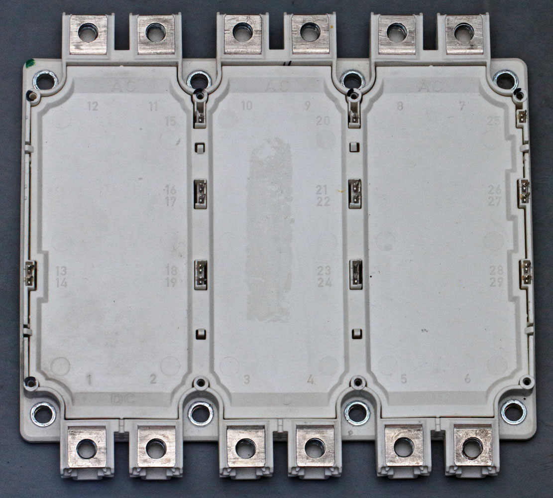
There are mounting holes to screw your gate driver board directly on top of the module. The low power pins are pressfit pins.

These modules are used a lot in motor inverters, photovoltaic inverters or USV.

(Thanks to capt bullshot!)


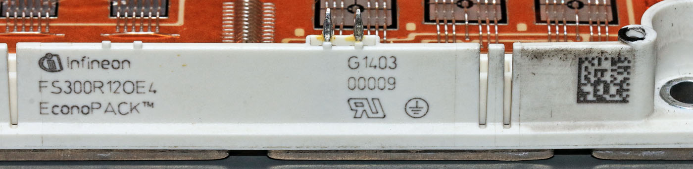
The name FS300R12OE4 contains a lot of information:
- FS: sixpack configuration
- 300: 300A maximum collector current
- R: reverse conducting
- 12: 1200V maximum Vce
- O: mechanical design
- E4: fast Trench-IGBTs with low Vcesat

The dot matrix code contains the number 00009 034011 80690664 1403
- 00009 is the Module Serial Number
- 034011 is the Module Material Number
- 80690664 is the Production Order Number
- 1403 is the date code
(datasheet information)

Datasheet tells you some more:
1200V is the maximum Vce. The isolation test voltage is 2,5kV. 300A are ok if the case is at 100°C. At 25°C a current of 460A is allowed. The package can dissipate up to 1650W. The thermal resistance between one IGBT and the case is just 0,091K/W (with isolation between IGBT and case!). Maximum peak current (1ms) is 600A. The module limits the short circuit current at 1200A (800V). At 150°C and 300A of collector current Vcesat is 2,05V. At 1200V the residual current can be up to 3mA.

Gate-Emitter-Voltage has to stay within +/-20V. At 15V the gate charge is 2,25µC. Datasheet tells us there is a integrated gate resistor with 2,5Ω. Input capacitance is 18,5nF. Reverse transfer capacitance is 1,05nF.

The freewheeling diode can conduct 300A too. At 300A and 25°C the forward voltage is 1,65V typ, 2,10V max.


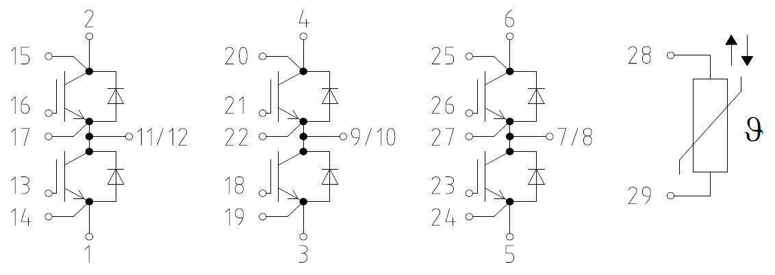
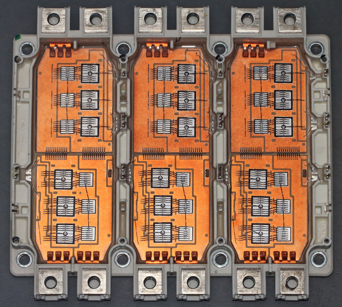
The datasheet shows the wiring of the module. Six IGBTs are connected as a B6 bridge. Parallel to the transistors are free-wheeling diodes. An NTC enables a temperature measurement.

Besides the absolutely necessary contacts the module has some auxiliary contacts. Each gate contact has a so-called auxiliary emitter. With this auxiliary emitter a clean gate-emitter voltage can be set which is just slightly distorted by the load current.

Further auxiliary contacts are located at the collectors of the upper transistors. Since the positive supply potential is present there it is possible to supply the gate driver circuit without much effort. An important function for the module itself is the so-called desaturation detection. This monitors the voltage drop across the IGBT. In the event of a problematically high current flow, the transistor leaves the saturation area and the voltage drop increases. If such a voltage rise occurs, the transistor can be shut down before damage occurs. The collectors of the lower transistors are accessible via the auxiliary emitters of the upper transistors.


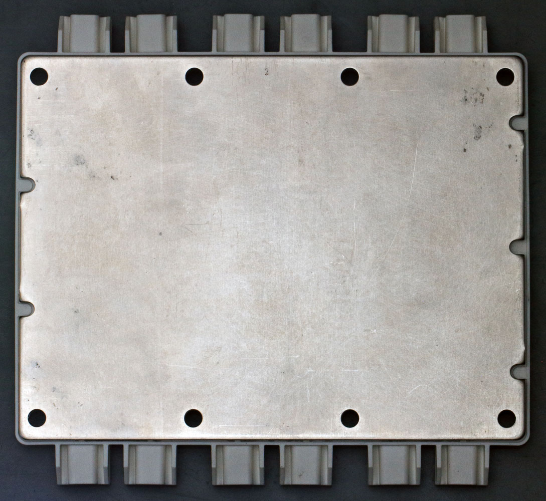
Quite a massive cooling plate.


There are eight hooks. Bending the hooks you can remove the top cover.


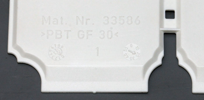
PBT GF30, Polybutylenterephthalat with 30% of fiberglass. PBT is similar to PET.


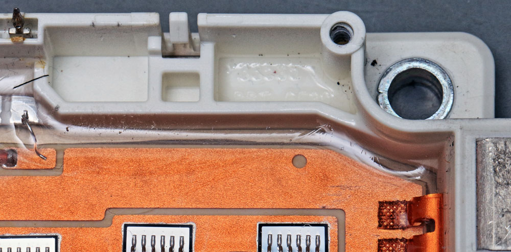
The active parts and the bondwires are protected with a transparent silicone gel potting.


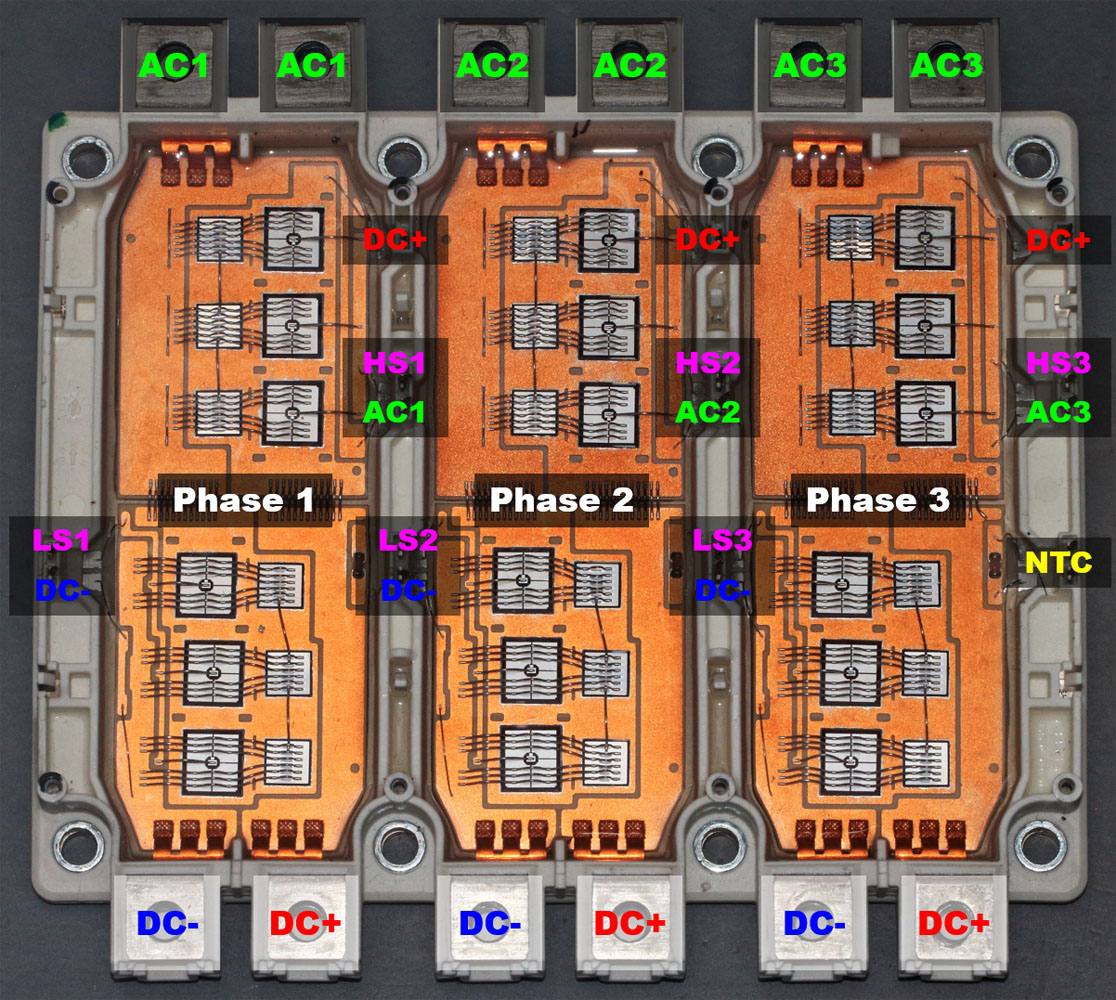
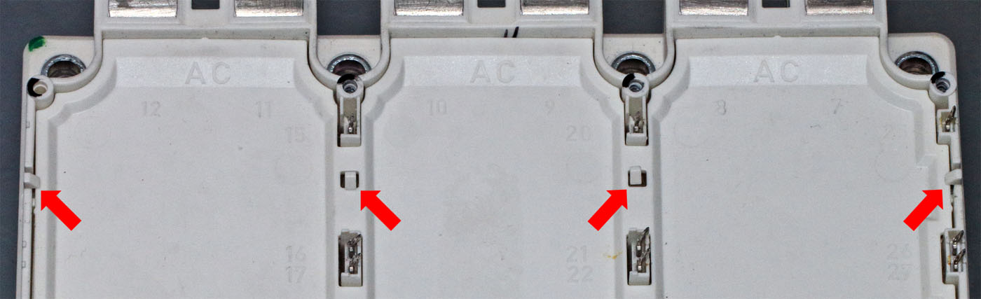
The three phases are clearly visible. Each phase is supplied individually via the two lower screw-on points. The two upper screw contacts represent the output of each push-pull stage.

On the left side of each phase the low-side transistors are controlled. The high-side transistors are controlled on the right side. Furthermore, DC-, DC+ and AC can be connected via press-fit contacts at each phase. On the right phase there are the contacts of the NTC, which is used for temperature measurement.


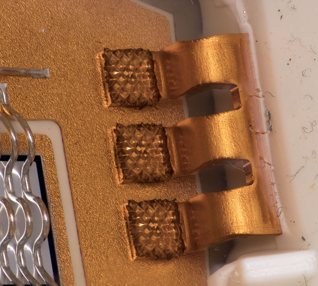
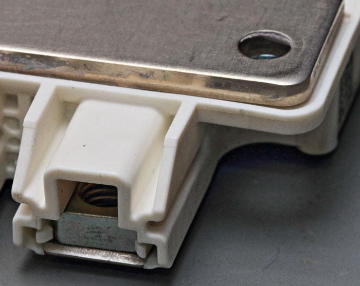
This is a high power contact! Datasheet states a lead resistance of 1,1mΩ.


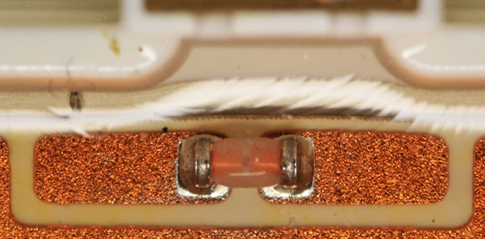
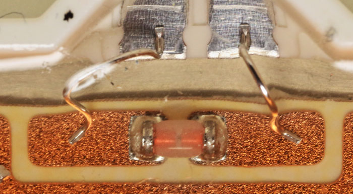
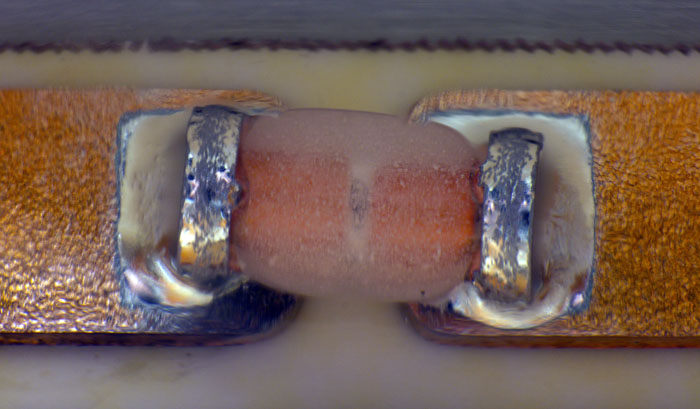
The NTC is packaged in a MELF housing. The temperature measurement is connected just at one phase, but the NTCs are present in each phase. In this way, each DBC can be set up in the same way. The temperature measurement just serves to check the temperature of the module approximately, local hot spots cannot be detected.


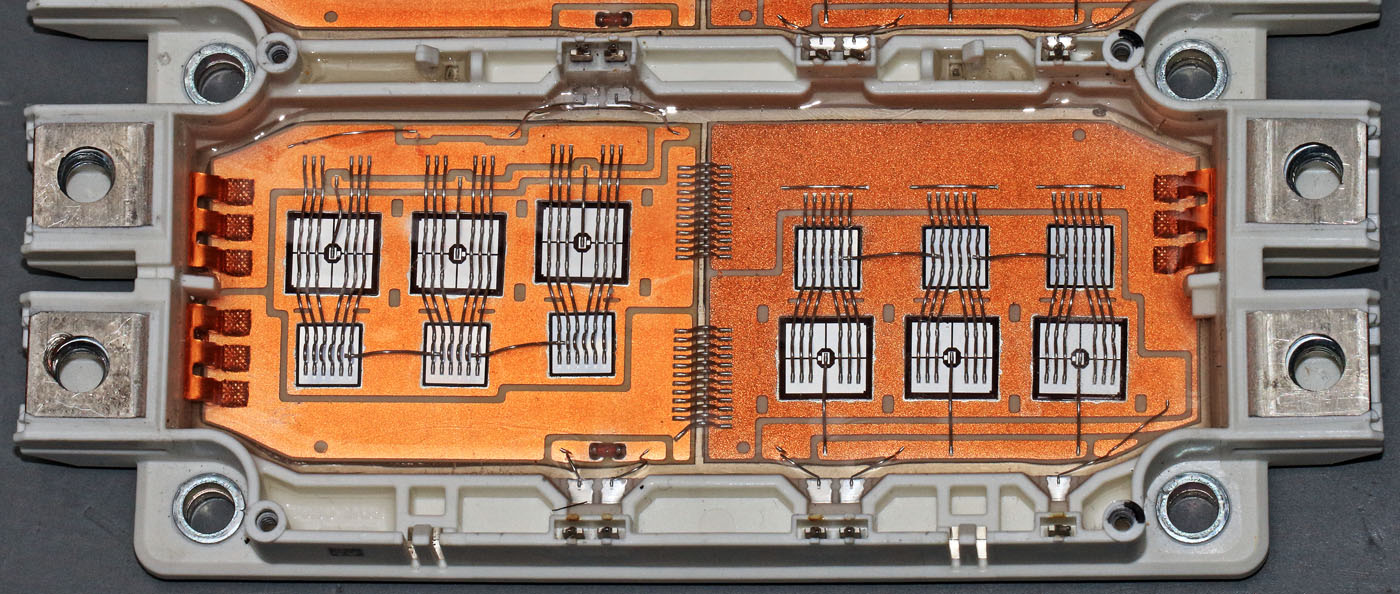
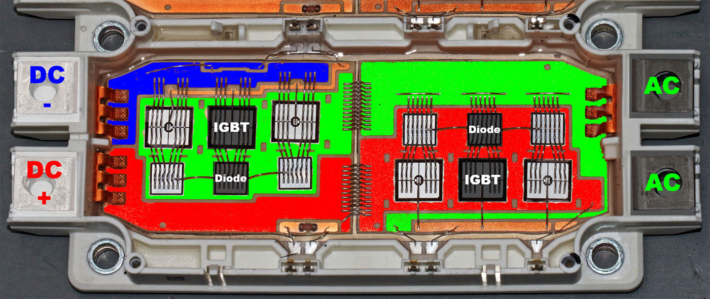
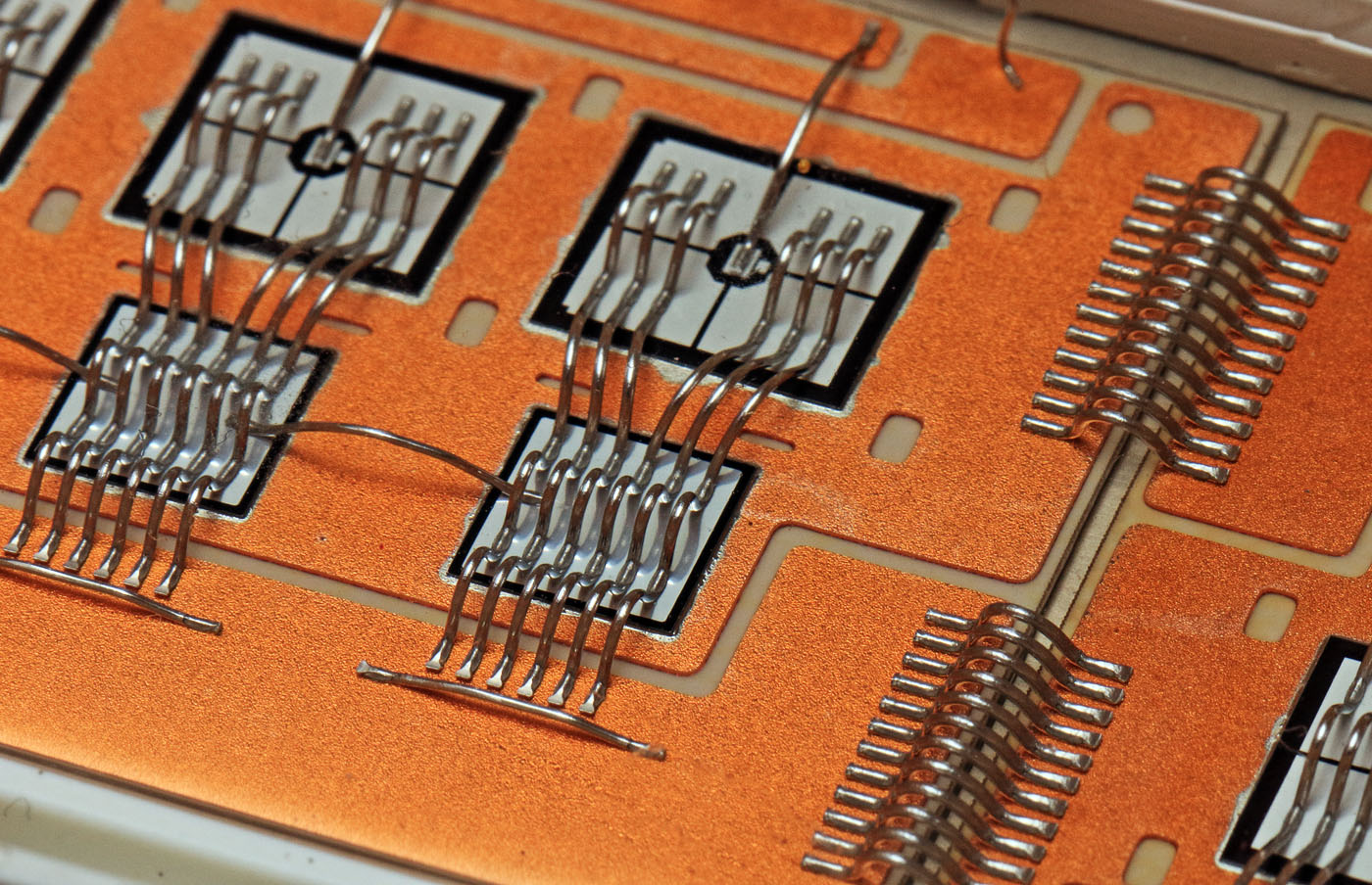
Each phase is composed of a lowside block (left) and a highside block (right). Lowside and highside each consist of three IGBT dies and three diode dies.

The arrangement of the components must meet many requirements. One important consideration is leakage inductance, which the datasheet specifies as typically 20nH. An inductance as low as possible reduces the switching losses. For this reason, among others, the DC link capacitor is usually directly and massively connected to the module. Another important point is a uniform current distribution across the individual transistors and, in the case of transient processes, also a uniform voltage distribution. Furthermore, the semiconductors have to be cooled reasonably evenly.


Here you can see the DBC a little better. The ceramic is aluminium oxide.


(...)

 
The following users thanked this post: SeanB, RoGeorge, Miyuki, capt bullshot

Offline NoopyTopic starter

  • Super Contributor
  • ***
  • Posts: 1730
  • Country: de
    • Richis-Lab
Re: Transistors - die pictures
« Reply #591 on: May 11, 2022, 04:00:19 pm »


Six bonding wires connect the emitters of each IGBTs with the free-wheeling diodes and the output or DC-.

The free-wheeling diodes are connected directly to each other with additional bonding wires. This connection reduces the effects of parasitic inductances, which can lead to unbalanced voltage loading between the three freewheeling diodes.

Unlike the lowside block, the highside block you can see here has additional bond wires above the freewheeling diodes. One can just speculate that the current distribution was optimized with this wires.


There is an additional copper island just to have a support point for the DC+ bonding wire.


The gate potentials of the IGBTs are contacted in the middle of the die and brought together via a copper strip.

If the module did not provide auxiliary emitters the reverse current of the gate drive would have to flow through the load path (above). This has several disadvantages. Contacting the load path is usually more complex from a interconnect perspective. In addition, the load current and the associated voltage drop affect the gate-emitter voltage. In addition, the detour via the load path increases the impedance in the gate drive.

Using the auxiliary emitter (below) significantly reduces gate circuit expansion. The press-fit pin of the auxiliary emitter reaches the gate drive directly next to the gate potential pin.

It is worth mentioning in this context that the auxiliary emitter pin is not directly connected to the emitter potential in front of it. Instead, the potential is routed a considerable distance to the left. This ensures similarly long leads for all three IGBTs connected in parallel. Such details are usually necessary so that the transistors switch sufficiently synchronously.


In the highside module, the gate circuit is slightly larger.


The bondwires are 400µm in diameter.


Infineon shows the design of the IGBT4 generation used here in the Application Note AN2018-14. These so-called trench field stop IGBTs have a gate electrode that not only rests on the surface but also runs in a trench, where it controls the MOSFET part of the IGBT more efficiently.

In addition, compared to the first generations, the collector was constructed differently so that the transistor could be made thinner. That reduced the saturation voltage. In the newer IGBT7 generation the structures have been further optimized.


A detailed picture of the setup can be found in the Infineon presentation "分立IGBT技术与特性总览“英飞凌杯”第二届嵌入式处理器和功率电子设计应用大奖赛".  ;D


Each IGBT die is 10.3mm x 9.4mm. The transistor is divided into four areas, all of which are contacted three times. In the middle is the gate contact.


The outer area of the die is protected by a thin potting material, probably a polyimide. The emitter contacts are clearly visible in the metal surface. The frame structure is used for E-field control. Dopants are introduced there in such a way that the electric field is as homogeneous as possible. Otherwise, local high field strengths could damage the structures and lead to failure in the long term.


The gate contact of the IGBT is located in the middle of the die. Although a gate resistor of 2.5Ω is specified in the datasheet, no resistor has been visible so far. With this in mind, it seems quite likely that the three stripes to the left of the bondpad represent this resistor. A certain minimum resistance is necessary to prevent oscillation tendencies. When high currents are switched very fast, high-frequency oscillations can occur and the feedback capacitance can switch the transistor on going into a deadly on/off state.

The cross-shaped structure conducts the gate potential throughout the die. To the right of the bondpad is an integrated test pad that appears to have been contacted in two places.

In the cross-shaped distribution network you can see a lot of vias. Through this vias the gate potential is transferred to the deeper polysilicon layer, which then ultimately feeds it to the individual IGBT cells.


The gate potential distribution does not go all the way to the edge. Just before the frame structure, the four emitter areas are connected.


The die is very thin so that it presents as little resistance as possible and heat can be removed as good as possible.


The edge length of the diode is 7,3mm.


The edges of the die are protected with a polyimide layer and the concentric frame structures can be seen.


According to the data sheet, the diodes are so-called "Emitter Controlled Diodes". One must not confuse these diodes with the switched diodes, which are described for example in the IEEE article "Power Diodes with Active Control of Emitter Efficiency". In this article you can find the above picture. There is a normal diode and a bipolar transistor connected in parallel. The bipolar transistor is controlled by a MOSFET structure. These diodes are called "Emitter Controlled Diode" too.

The term "Emitter Controlled Diode" is used at the same time for diodes which just have a somewhat optimized distribution of doping and thus switch less snappy.


https://www.richis-lab.de/BipolarA04.htm

 :-/O
 
The following users thanked this post: SeanB, SilverSolder, RoGeorge, mawyatt

Online T3sl4co1l

  • Super Contributor
  • ***
  • Posts: 21658
  • Country: us
  • Expert, Analog Electronics, PCB Layout, EMC
    • Seven Transistor Labs
Re: Transistors - die pictures
« Reply #592 on: May 11, 2022, 11:45:32 pm »
Very cool!

It occurs to me, the housing is not only easy to remove and not exactly tightly sealed, but also during testing, you might have one of these open and accessible to IR camera or thermocouple probing -- so the dies may be exposed to light, and a black-filled passivation/potting on the dies is probably a good idea.

You can also special-order them without the gorilla-snot filling, to facilitate such probing.

Tim
Seven Transistor Labs, LLC
Electronic design, from concept to prototype.
Bringing a project to life?  Send me a message!
 
The following users thanked this post: Noopy

Online mawyatt

  • Super Contributor
  • ***
  • Posts: 3240
  • Country: us
Re: Transistors - die pictures
« Reply #593 on: May 12, 2022, 01:50:53 pm »
Thats some serious power handling capability and it shows with the multiple bond wires and package/substrate.

In your statement:

"There is an additional copper island just to have a support point for the DC+ bonding wire."

There's an associated image just above that shows a bond wire looping from one pad to another. The bond wire appears to neck down and possibly open. Is this actually open or just an image artifact?

Nice images as usual :-+

Best,
Curiosity killed the cat, also depleted my wallet!
~Wyatt Labs by Mike~
 

Offline NoopyTopic starter

  • Super Contributor
  • ***
  • Posts: 1730
  • Country: de
    • Richis-Lab
Re: Transistors - die pictures
« Reply #594 on: May 12, 2022, 08:21:03 pm »
Thanks!  8)

The strange area of this bondwire is just an image artifact due to the silicone potting.
Actually that is a "normal" picture, no image stacking done, just f/16.  :-/O

Offline doktor pyta

  • Frequent Contributor
  • **
  • Posts: 488
  • Country: pl
Re: Transistors - die pictures
« Reply #595 on: May 17, 2022, 05:38:58 pm »
 
The following users thanked this post: SeanB, RoGeorge, Miyuki, JPortici

Online RoGeorge

  • Super Contributor
  • ***
  • Posts: 6185
  • Country: ro
Re: Transistors - die pictures
« Reply #596 on: May 17, 2022, 05:58:54 pm »
Wow!  8)
Didn't know 20W can do that!

The next video in that YT channel, "DIY-Optics dot com", is laser etching copper clad for a PCB coil.  :o

Offline NoopyTopic starter

  • Super Contributor
  • ***
  • Posts: 1730
  • Country: de
    • Richis-Lab
Re: Transistors - die pictures
« Reply #597 on: May 17, 2022, 06:04:43 pm »


Nice! ...but there is still a little "dirt" left...  ;)

Offline NoopyTopic starter

  • Super Contributor
  • ***
  • Posts: 1730
  • Country: de
    • Richis-Lab
Re: Transistors - die pictures
« Reply #598 on: May 17, 2022, 06:39:40 pm »


For this one you would need a laser with a little more power.  ;D

RCA called the 2N6254 "premium type from 2N3055 family". It´s a hometaxial transistor (some more information here: https://www.richis-lab.de/2N3055_08.htm).

Vceo can go up to 85V compared to 70V in case of the 2N3055. The maximum collector current is specified with 7A continously and 15A peak. Pmax is 150W, where the 2N3055 just can handle up to 115W.


Typical for a hometaxial transistor is the robustness against second breakdown. The SOA of the 2N6254 is actually just limited by the maximum current, the maximum voltage and the maximum power dissipation.


In case of RCA's 2N3055, which is also hometaxial, the SOA range is additionally limited by the second breakdown, even if it is just a very small area that has to be avoided.


The design of the transistor strongly reminds one of the RCA 2N3055H, which was also manufactured in 1979 (https://www.richis-lab.de/2N3055_05.htm). It is quite likely that both transistors were based on the same design and then binned according to their specifications.


The die shows the familiar structure of a hometaxial transistor. The current is distributed via a solder layer on top of which the contact plates are directly soldered.


In the lower left corner the solder layer is discolored. Most likely very high temperatures occurred here due to damage.


Yeah, the junction is dead in the lower left corner.


A typical hometaxial structure.


https://www.richis-lab.de/BipolarA05.htm

 :-/O
 
The following users thanked this post: SeanB, RoGeorge, floobydust

Online T3sl4co1l

  • Super Contributor
  • ***
  • Posts: 21658
  • Country: us
  • Expert, Analog Electronics, PCB Layout, EMC
    • Seven Transistor Labs
Re: Transistors - die pictures
« Reply #599 on: May 17, 2022, 07:51:08 pm »
Love the crystal growth pattern on that solder.  Pure tin I suppose?  Oh, or would they use lead because high temp handling?

Also, if it were tin... whisker growth?  But it looks pretty clean... :D

Tim
Seven Transistor Labs, LLC
Electronic design, from concept to prototype.
Bringing a project to life?  Send me a message!


Share me

Digg  Facebook  SlashDot  Delicious  Technorati  Twitter  Google  Yahoo
Smf