Author Topic: Transistors - die pictures  (Read 188289 times)

0 Members and 2 Guests are viewing this topic.

Offline floobydust

  • Super Contributor
  • ***
  • Posts: 6958
  • Country: ca
Re: Transistors - die pictures
« Reply #600 on: May 17, 2022, 11:52:54 pm »
The pattern looks soft though, maybe from an abrasive wash and the maze reminds me of bismuth crystallization a bit.
SOA 2A@80V gee this part was tough, hard to find something like that nowadays.
 

Offline NoopyTopic starter

  • Super Contributor
  • ***
  • Posts: 1729
  • Country: de
    • Richis-Lab
Re: Transistors - die pictures
« Reply #601 on: May 18, 2022, 03:36:51 am »
Well I don´t know what is causing the nice pattern.  :-//


I have update the transistor sorting:

Now we can go on...  8)
 
The following users thanked this post: MegaVolt

Offline T3sl4co1l

  • Super Contributor
  • ***
  • Posts: 21658
  • Country: us
  • Expert, Analog Electronics, PCB Layout, EMC
    • Seven Transistor Labs
Re: Transistors - die pictures
« Reply #602 on: May 18, 2022, 12:14:49 pm »
Also, the pattern seems to be aligned over quite a range of distance, maybe even the entire layer; but not to the substrate, the emitter and base blobs are aligned differently.  Possibly seeded by the contact point, whatever orientation started there?  Whatever they did, it probably cooled fairly slowly!

The texture isn't usually very aggressive, for example I've melted bars of fairly pure aluminum (electrical cable) and it grows a soft pattern of dendritic crystals on the free surface.  The first crystals to form, extend up to the molten surface; as it cools, the surrounding liquid shrinks, exposing the first crystals (while they grow a bit more), and other random crystallites intergrow around them.  It's a neat pattern, but not very deep.  (You get distinctive bismuth crystals by seeding growth, then removing it from solution before randomly seeded intergrowth starts.)

Tim
Seven Transistor Labs, LLC
Electronic design, from concept to prototype.
Bringing a project to life?  Send me a message!
 

Offline NoopyTopic starter

  • Super Contributor
  • ***
  • Posts: 1729
  • Country: de
    • Richis-Lab
Re: Transistors - die pictures
« Reply #603 on: May 22, 2022, 07:40:38 pm »


The GD180 is a germanium transistor with a voltage rating of 60V. It can conduct up to 3A. The letter at the end of the name stands for the hfe of the transistor (A: 18-35, B: 28-56, C: 45-90). The maximum junction temperature is just 75°C. The maximum power dissipation is 5,3W. The cutoff frequency is at least 250kHz.


There is an imprinting in the base plate. Inside it forms a base on which the transistor is placed.


A large white plate was inserted into the housing to bind any moisture that may occur.


Two sheets of metal connect the pins of the package with the transistor. At the pins the metal sheets are bent at an angle of 90°. The design reminds me of the Tesla OC26 (https://www.richis-lab.de/Bipolar94.htm). Matching the occurring currents, the sheet metal element at the emitter is significantly thicker than the one at the base.

The base plate is made of copper which ensures an optimal heat dissipation.


Basically it is the normal structure of a germanium transistor. The surfaces are covered with a thin clear protective coating.

Metal chips can be seen at the front edge of the emitter sheet, which most likely occurred while the case was opened.


There are two different solders on the emitter side of the germanium disk. The lower solder is rather yellowish. Usually this solder contains indium and thus serves as a p-dopant. For the contacting of the emitter sheet another rather silver solder was used.

On the germanium disk under the yellowish solder something can be seen that looks like a thin coating.


Does anybody know what that is?  :-//


https://www.richis-lab.de/BipolarA06.htm

 :-/O
 
The following users thanked this post: SeanB, SilverSolder, RoGeorge

Offline NoopyTopic starter

  • Super Contributor
  • ***
  • Posts: 1729
  • Country: de
    • Richis-Lab
Re: Transistors - die pictures
« Reply #604 on: June 08, 2022, 08:45:01 pm »


This transistor is used for the development of hybrid circuits, such as the DAC 32 is one (https://www.richis-lab.de/DAC03.htm). The logo identifies the transistor as a component of the Russian manufacturer Pulsar. No further information can be found. I assume the type designation consists just of the characters A479A. 67 could refer to the year 1967.  :-// The component tester says it is a silicon NPN transistor.


If you remove the outer packaging, the transistor with its bondwires is still protected by two plastic discs.


The development model of the double transistor K1NT291B is equipped with a tube socket so that it can be measured before installation (https://www.richis-lab.de/Bipolar71.htm).

Here, the bondwires are connected with thicker connecting wires, which in turn are anchored in one of the plastic disks.

For integration into a hybrid circuit, the thin bondwires are cut, the transistor is inserted into the circuit to be built up and the bondwires are connected to the circuit.


The transistor itself has an edge length of round about 1mm and it is protected from environmental conditions by a red potting on both sides.


After removing the potting there remain some residues. Perhaps irregularities in the surface contribute to this irregularities. You need some hydrofluoric acid to remove most of the contamination. Unfortunately the acid removes the colourful  light resonances too. There are still some irregularities on the surface.


The component tester shows where to find collector, base and emitter.

The large contact on the left of the die is not the collector, as you would expect, but the base terminal.

The center square appears to be a via that allows to contact a deeper collector layer. Above this is the base layer.

The right square has to contain the emitter area, which is embedded in the base layer.


https://www.richis-lab.de/BipolarA07.htm

 :-/O
 
The following users thanked this post: SeanB, RoGeorge

Offline RoGeorge

  • Super Contributor
  • ***
  • Posts: 6185
  • Country: ro
Re: Transistors - die pictures
« Reply #605 on: June 09, 2022, 05:11:21 am »
 :o
Wow!  Never seen something alike.  At first I thought it's a resonator, or a SAW (Surface Acoustic Wave) filter.

Offline MegaVolt

  • Frequent Contributor
  • **
  • Posts: 917
  • Country: by
Re: Transistors - die pictures
« Reply #606 on: June 09, 2022, 09:54:31 am »
No further information can be found. I assume the type designation consists just of the characters A479A. 67 could refer to the year 1967.  :-// The component tester says it is a silicon NPN transistor.
The marking of the transistor is non-standard, which means an experimental sample. The first letter "А" (Cyrillic) denotes the plant - Pulsar. "А479А" (Cyrillic) is most likely a prototype of the transitor 2Т319А (Cyrillic).

Here is information about it: http://www.155la3.ru/2tp319.htm
 
The following users thanked this post: RoGeorge, Noopy

Offline MegaVolt

  • Frequent Contributor
  • **
  • Posts: 917
  • Country: by
Re: Transistors - die pictures
« Reply #607 on: June 09, 2022, 09:56:30 am »
Here is an example of a hybrid assembly with similar transistors http://www.155la3.ru/111_k11gi04_31v.htm
 
The following users thanked this post: RoGeorge, Noopy

Offline NoopyTopic starter

  • Super Contributor
  • ***
  • Posts: 1729
  • Country: de
    • Richis-Lab
Re: Transistors - die pictures
« Reply #608 on: June 09, 2022, 12:04:12 pm »
No further information can be found. I assume the type designation consists just of the characters A479A. 67 could refer to the year 1967.  :-// The component tester says it is a silicon NPN transistor.
The marking of the transistor is non-standard, which means an experimental sample. The first letter "А" (Cyrillic) denotes the plant - Pulsar. "А479А" (Cyrillic) is most likely a prototype of the transitor 2Т319А (Cyrillic).

Here is information about it: http://www.155la3.ru/2tp319.htm

Thanks for you input!  :-+
How do you get from A479A to 2T319A?

Offline MegaVolt

  • Frequent Contributor
  • **
  • Posts: 917
  • Country: by
Re: Transistors - die pictures
« Reply #609 on: June 09, 2022, 12:45:03 pm »
How do you get from A479A to 2T319A?
Google gives out some information from a closed forum. Plus the production years are similar.
 
The following users thanked this post: Noopy

Offline mawyatt

  • Super Contributor
  • ***
  • Posts: 3239
  • Country: us
Re: Transistors - die pictures
« Reply #610 on: June 09, 2022, 01:37:50 pm »
Interesting, didn't know anyone else had used these type of transistors. Recall GE back in 60s had a similar line of transistor die with wire bonds leads and the bonded die dipped in epoxy. These were also used in small hybrids.

Thanks for showing.

Best,
Curiosity killed the cat, also depleted my wallet!
~Wyatt Labs by Mike~
 

Offline NoopyTopic starter

  • Super Contributor
  • ***
  • Posts: 1729
  • Country: de
    • Richis-Lab
Re: Transistors - die pictures
« Reply #611 on: June 30, 2022, 03:20:08 am »


Today just another small 2N2222A.
SGS - The transistor was built into a modul manufactured in 1984 so it has to be SGS ATES.


The edge length is 0,42mm.


https://www.richis-lab.de/BipolarA08.htm

 :-/O
 
The following users thanked this post: SeanB, RoGeorge, floobydust

Offline NoopyTopic starter

  • Super Contributor
  • ***
  • Posts: 1729
  • Country: de
    • Richis-Lab
Re: Transistors - die pictures
« Reply #612 on: August 08, 2022, 07:10:17 am »


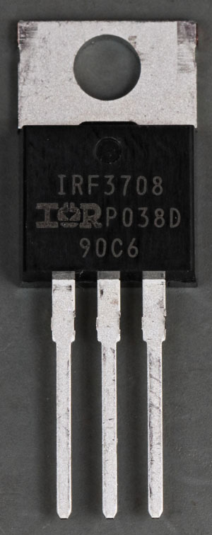
I ordered a IRF3708 at Reichelt and in my view that is a counterfeit part. The IRF3708 is a common power MOSFET which is now obsolete and because of that it´s hard to get genuine parts.

The IRF3708 offers a blocking voltage of 30V and conducts up to 62A permanently with a Rdson of 12mΩ. A peak current of 248A is possible. 4,5V Vgs is already sufficient to turn the MOSFET on almost completely.


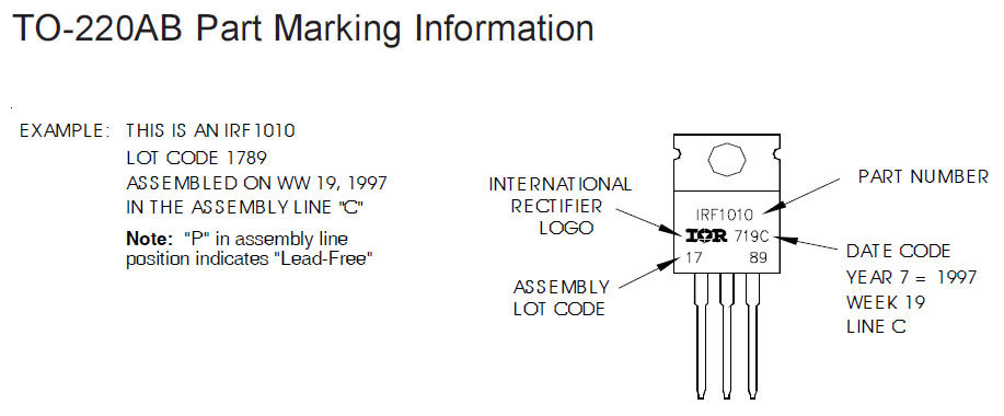
The datasheet contains a drawing that shows how the marking of the IRF3708 should look like.


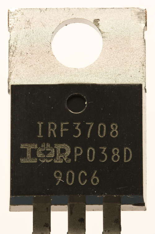
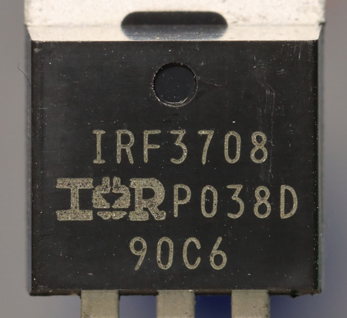
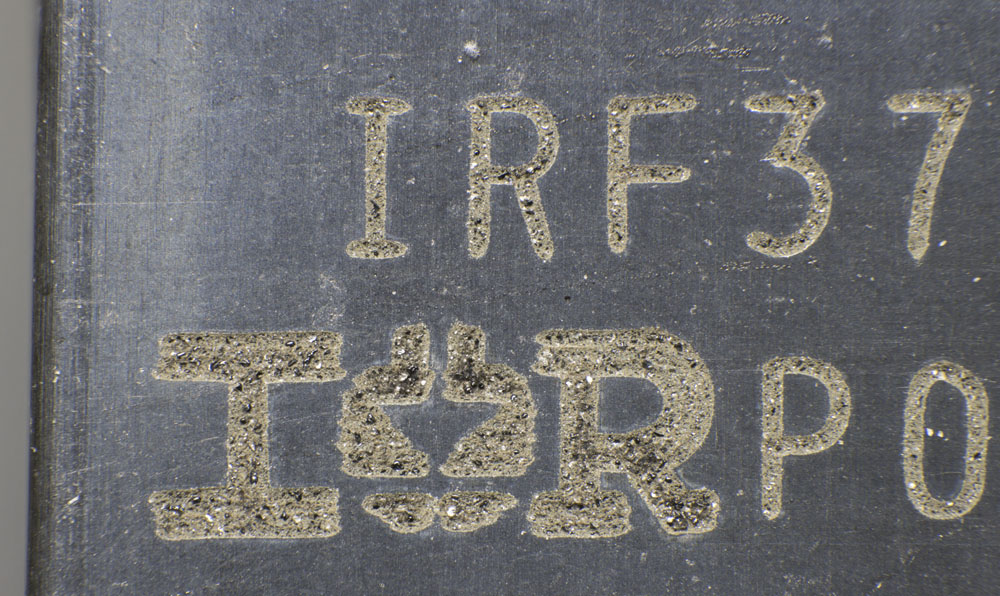
The marking of the present IRF3708 shows two clear deviations compared to the drawing in the datasheet. The characters in the bottom line are not shown in pairs on the left and right side but together in the center. However, the International Rectifier logo is particularly striking. Superficially it is well done but a closer look reveals a cylindrical bulge at the top of the circle that the original logo does not have.

The cuts in the cooling fin are less pronounced than shown in the drawing in the datasheet. However, they are not specified there either.


There are no grinding marks on the surface.

In detail the laser inscription looks unclean. The mold material seems to be burned in some places.


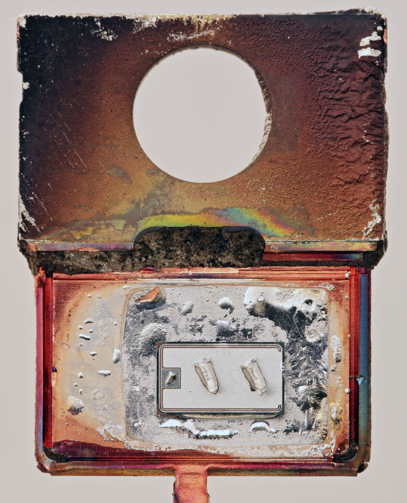
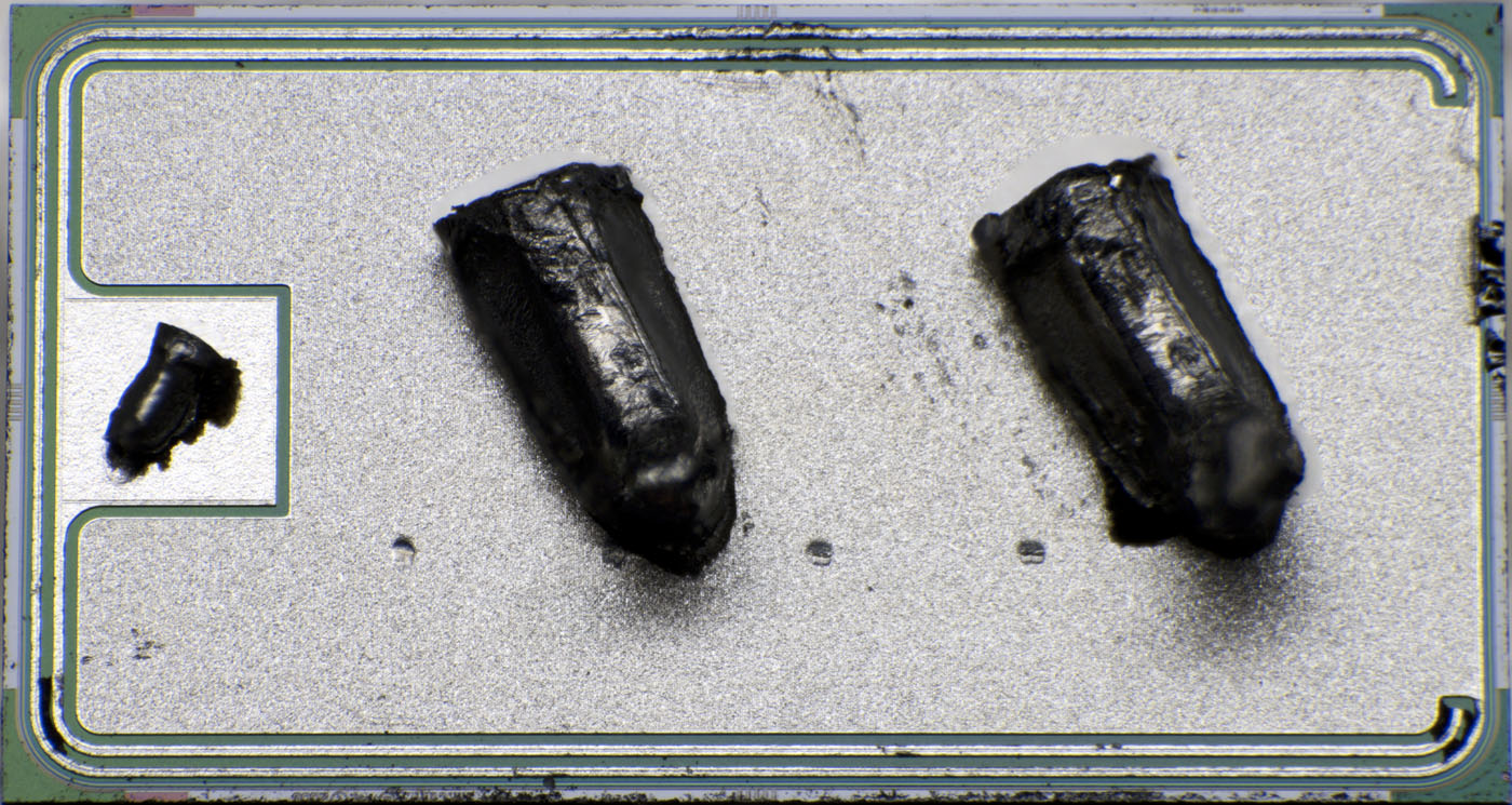
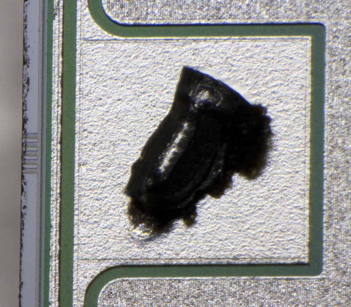
The case contains a die with dimensions of 3,6mm x 2,0mm. Two bondwires contact the upper metal layer. The imprints of test pins can still be seen. The gate potential is distributed over the die with one wire each at the upper and lower edge.


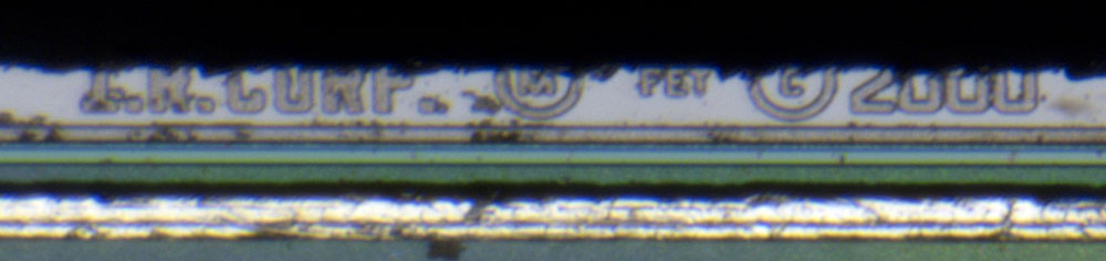
On the bottom edge of the die there are the remnants of some letters. "I.R.CORP." reveals that it is indeed a International Rectifier MOSFET. The same abbreviation is found in the IGBT IRG4PH40K (https://www.richis-lab.de/Bipolar35.htm). It remains questionable whether it is an IRF3708. The design obviously dates back to the year 2000.


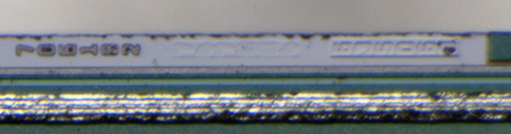
As with the IRG4PH40K mask designations are shown on the upper edge, but these do not allow any conclusion to be drawn about the transistor type.


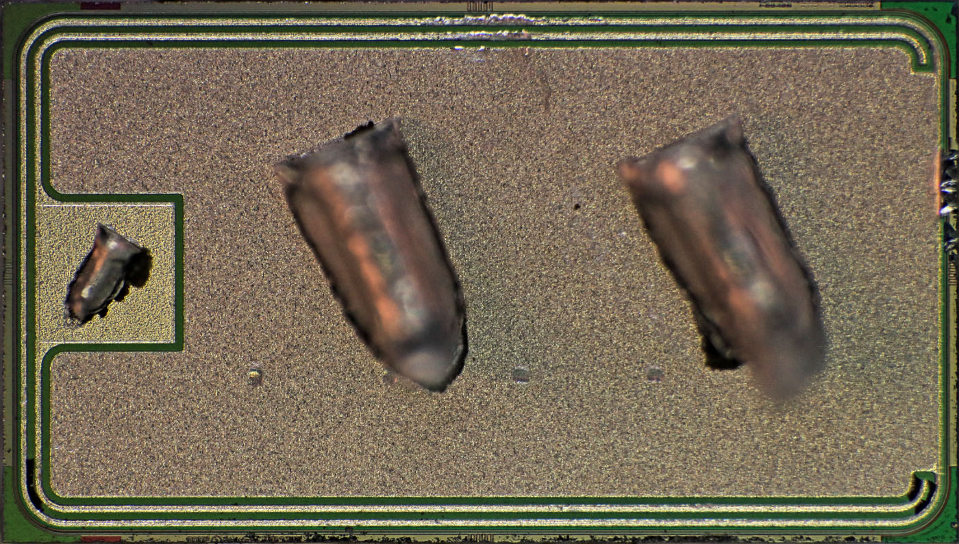
The upper metal layer is relatively thick. Vertical structures are visible on the surface of the source area.


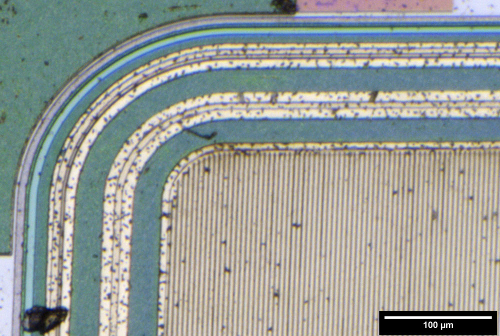
If the metal layer is removed with hydrochloric acid, the structure of the individual MOSFETs becomes more prominent. The bright stripes are about 3µm wide and keep a distance of about 1µm. The bright areas contact the source areas. In the dark areas there are the gate structures.


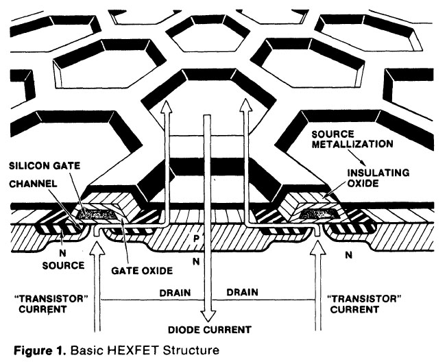
The "International Rectifier HEXFET Databook" shows that a HEXFET like the IRF3708 should have a honeycomb structure. The striped structure that can be seen in the present transistor makes it very likely it´s a counterfeit.


https://www.richis-lab.de/FET23.htm

 :-/O
« Last Edit: August 08, 2022, 09:28:35 am by Noopy »
 
The following users thanked this post: SeanB, RoGeorge

Online magic

  • Super Contributor
  • ***
  • Posts: 6758
  • Country: pl
Re: Transistors - die pictures
« Reply #613 on: August 08, 2022, 08:24:57 am »
I initially read "Rochester" and was like :wtf: :wtf: :wtf:

The logo is dodgy as hell.
I wonder if the word "hexfet" still means anything in IR datasheets.
Does anyone know IR part numbers that aren't advertised as "hexfet", which this device could really be?

<tinfoil hat on>
Maybe the die wasn't made by IR ;D
 

Offline NoopyTopic starter

  • Super Contributor
  • ***
  • Posts: 1729
  • Country: de
    • Richis-Lab
Re: Transistors - die pictures
« Reply #614 on: August 08, 2022, 09:33:39 am »
This was my thought too: Is a HEXFET today still a HEXFET?  :-+

Offline NoopyTopic starter

  • Super Contributor
  • ***
  • Posts: 1729
  • Country: de
    • Richis-Lab
Re: Transistors - die pictures
« Reply #615 on: August 08, 2022, 01:20:47 pm »
By the way:
A short measurement of the Rdson showed 10mOhm at 4,5V at 4A. Not bad at all...

Online magic

  • Super Contributor
  • ***
  • Posts: 6758
  • Country: pl
Re: Transistors - die pictures
« Reply #616 on: August 08, 2022, 03:03:43 pm »
But the logo looks fake. What's the breakdown voltage? Gate capacitance?
 

Offline NoopyTopic starter

  • Super Contributor
  • ***
  • Posts: 1729
  • Country: de
    • Richis-Lab
Re: Transistors - die pictures
« Reply #617 on: August 08, 2022, 03:47:06 pm »
The logo is very strange!  ;D

Quick&Dirty:

Breakdown voltage: 35V

Rdson (@4A):
Ugs=2,8V => 12mOhm
Ugs=4,5V => 10mOhm

Cgs=2,88nF (@1kHz, D-S open, HP4261A)

Offline T3sl4co1l

  • Super Contributor
  • ***
  • Posts: 21658
  • Country: us
  • Expert, Analog Electronics, PCB Layout, EMC
    • Seven Transistor Labs
Re: Transistors - die pictures
« Reply #618 on: August 08, 2022, 04:32:15 pm »
Sounds like Vgs(th) is on the low side of normal, hence the relatively low Rds(on). Lower Id also contributes (Fig.12), although maybe not by much given the scale of that plot, hah.

Etching definitely looks bad, but also doesn't seem to be a refurbished (used) part -- plating looks new, matte tin.  (Or is there a process to reproduce that on used parts?).  3-digit date code doesn't seem like it would reward updating the label, either.  And "IR" on the die confirms it's, at worst, a remarked part, with very similar characteristics as it turns out; or a much more exact die clone than anyone should bother with(!?).

Although I have, presumably authentic, IR parts, 2007 date?, that are bright tin (or maybe solder, PbF type in any case), but IR probably used both depending on product/packaging line.  I just forget if I've seen them use matte tin elsewhere, from those years.

Tim
Seven Transistor Labs, LLC
Electronic design, from concept to prototype.
Bringing a project to life?  Send me a message!
 

Offline NoopyTopic starter

  • Super Contributor
  • ***
  • Posts: 1729
  • Country: de
    • Richis-Lab
Re: Transistors - die pictures
« Reply #619 on: August 08, 2022, 04:50:11 pm »
It was a quick&dirty measurement, so there will be some error in the numbers.

IR markings are strange...
Do you remember these IGBTs: https://www.richis-lab.de/Bipolar35.htm
A bad and a really bad marking but the silicon seemed genuine.
Is there a second backend for lower quality stuff? Or is someone collecting "still good" scrapped parts and provides them with a self made marking? Perhaps tolerated by IR? No...  ???
« Last Edit: August 08, 2022, 04:51:43 pm by Noopy »
 

Offline NoopyTopic starter

  • Super Contributor
  • ***
  • Posts: 1729
  • Country: de
    • Richis-Lab
Re: Transistors - die pictures
« Reply #620 on: August 08, 2022, 09:14:58 pm »
Thank you for your offer but since I have way too much parts here I have to decline. In these modern digital MCUs we won't see very much details.
 
The following users thanked this post: karpouzi9

Offline NoopyTopic starter

  • Super Contributor
  • ***
  • Posts: 1729
  • Country: de
    • Richis-Lab
Re: Transistors - die pictures
« Reply #621 on: August 09, 2022, 07:43:56 pm »


One Two more strange IRF3708.

Of the two IRF3708 becomes conductive at a Ugs of 3V. The datasheet of the IRF3708 specifies a maximum of 2,0V. The other MOSFET shows a much too high leakage current of 2mA at Ugs=0V. (Measured by someone else.)

The two transistors are marked the same way. Depending on the light the letters are sometimes very hard to see. If you look at the characters more closely, you can see slight differences in the shapes. One package also appears somewhat darker than the other.


Viewed in the right light ridges stand out that were almost certainly created while the surface was sanded.


Some areas are burned a little too much.


On the left edge the color seem a little inhomogeneous probably due to bad painting after sanding.


And at the underside of the package we can see the paint residues.


Both transistors contain the same type of die.


The die is 3,9mm x 2,5mm. The source area is contacted with two bonding wires.


The transistor is divided in two parts. The gate potential is distributed via a metal frame which encloses the two source areas.


On the left edge there are the remaining of test structures, but they do not give a direct indication what was the manufacturer or the transistor type.


If you look very closely, you can see very thin horizontal structures in the source area.


https://www.richis-lab.de/FET24.htm

 :-/O
 
The following users thanked this post: SeanB, karpouzi9

Offline NoopyTopic starter

  • Super Contributor
  • ***
  • Posts: 1729
  • Country: de
    • Richis-Lab
Re: Transistors - die pictures
« Reply #622 on: August 11, 2022, 07:03:41 pm »


And another strange IRF3708. First Drain current occurs at a Gate-Source-Voltage of 3,0V. That´s not normal.


The marking does not correspond to the pattern shown in the datasheet. In addition, the letters are rather unclean.


The die took some damage. The dimensions are 3,3mm x 2,4mm.

Source is contacted with two bondwires. Relatively long sections rest on the metal layer.


The gate potential is distributed via wires on the upper and lower edges of the die.

Through the metal layer no special structure is visible.


https://www.richis-lab.de/FET25.htm

 :-/O

Offline NoopyTopic starter

  • Super Contributor
  • ***
  • Posts: 1729
  • Country: de
    • Richis-Lab
Re: Transistors - die pictures
« Reply #623 on: August 21, 2022, 05:09:05 pm »


That´s an old one!
The Texas Instruments 2N389 is said to be the first freely available silicon power transistor. In the Electronic Design magazine from 1957 (Volume 5 Issue 12) the 2N389 is advertised as new. The present component dates from 1966.

The 2N389 isolates up to 60V (Rbe=33Ω). The collector provides a current carrying capacity of at least 1,5A. Some documents state 2A or even 3A. The datasheet specifies a current gain of 12 to 60 and still guarantees at least a factor of 8 at -55°C. The operating temperature range is very wide at -65°C to 200°C (junction temperature). At 25°C case temperature the 2N389 can dissipate 85W. The cutoff frequency is in the range of 8MHz.


"GN", "2", "3", whatever that means...  :-//
The pins form hooks.


The construction inside the case seems quite modern for its age.


The die is placed on a socket and is contacted with thick bondwires.


The bondwires are not directly welded to the connection pins. There is a metal plate between them.

At this point you can clearly see that the transistor is covered with a thin protective lacquer. Below the bondwire there are larger accumulations of this varnish.


The edge length of the die is 6,4mm. Base and emitter areas interlock. The emitter contact is slightly wider than the base contact. There are minor scratches and dirt on the metallization.


The bond tool has left an unusual imprint on the bondwire.


The 2N389 is a MESA transistor where the silicon is etched down at the edge to create a clean base-collector junction edge. This increases the voltage rating.

The protective varnish has not wetted the entire die. At the edges the silicon surface is exposed.


The junction between base and emitter is clearly visible. Edges stand out at the edges of the metallization. It could be that these are breakthroughs through a protective oxide layer. Perhaps these areas made the protective coating necessary. It would cover gaps between the metal layer and the silicon oxide layer.


The base-emitter junction breaks down at -14V. The datasheet guarantees a dielectric strength of at least -10V. This is a high value for an epitaxial transistor, which indicates a relatively low doping typical for its age. The weak doping certainly is one reason why the 2N389 could be specified for relatively high junction temperatures.

In the upper image the current is 0,1A. The current distribution appears uniform. There are no particular glitches to be seen. In the lower image the current is 1A.


https://www.richis-lab.de/BipolarA09.htm

 :-/O
 
The following users thanked this post: SeanB, SilverSolder, RoGeorge, ch_scr

Offline T3sl4co1l

  • Super Contributor
  • ***
  • Posts: 21658
  • Country: us
  • Expert, Analog Electronics, PCB Layout, EMC
    • Seven Transistor Labs
Re: Transistors - die pictures
« Reply #624 on: August 22, 2022, 01:24:22 am »
Wow, mastered it in 1955!  Well, at what yields, is the real question... :D

Tim
Seven Transistor Labs, LLC
Electronic design, from concept to prototype.
Bringing a project to life?  Send me a message!


Share me

Digg  Facebook  SlashDot  Delicious  Technorati  Twitter  Google  Yahoo
Smf