Author Topic: Transistors - die pictures  (Read 190685 times)

0 Members and 3 Guests are viewing this topic.

Offline NoopyTopic starter

  • Super Contributor
  • ***
  • Posts: 1734
  • Country: de
    • Richis-Lab
Re: Transistors - die pictures
« Reply #650 on: December 05, 2022, 07:42:51 pm »


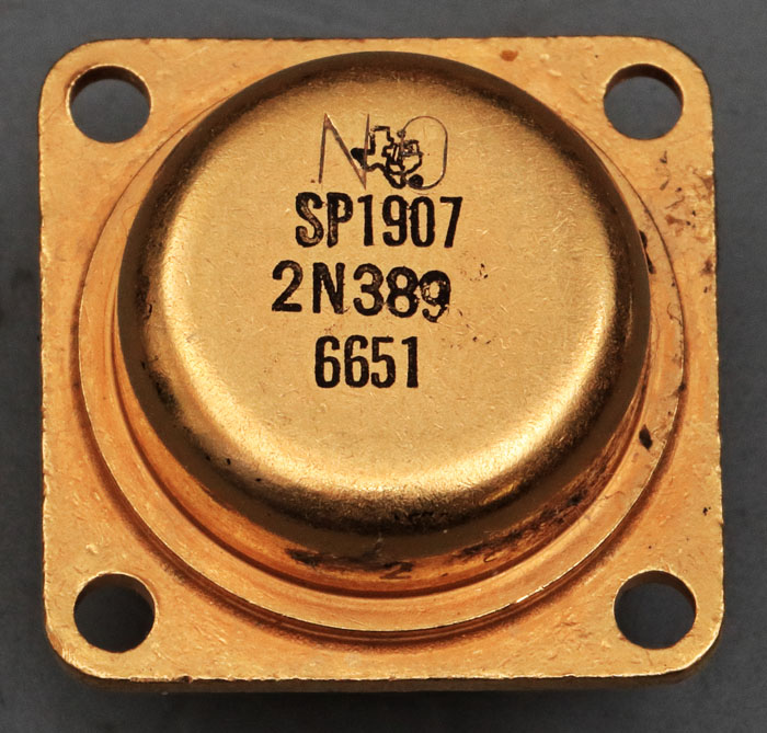
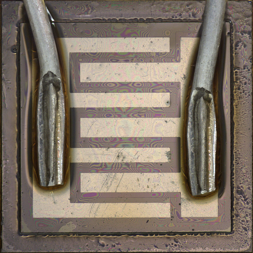
I once again took the 2N389 with its wide gap between the base and the emitter metallization and took some IR pictures...


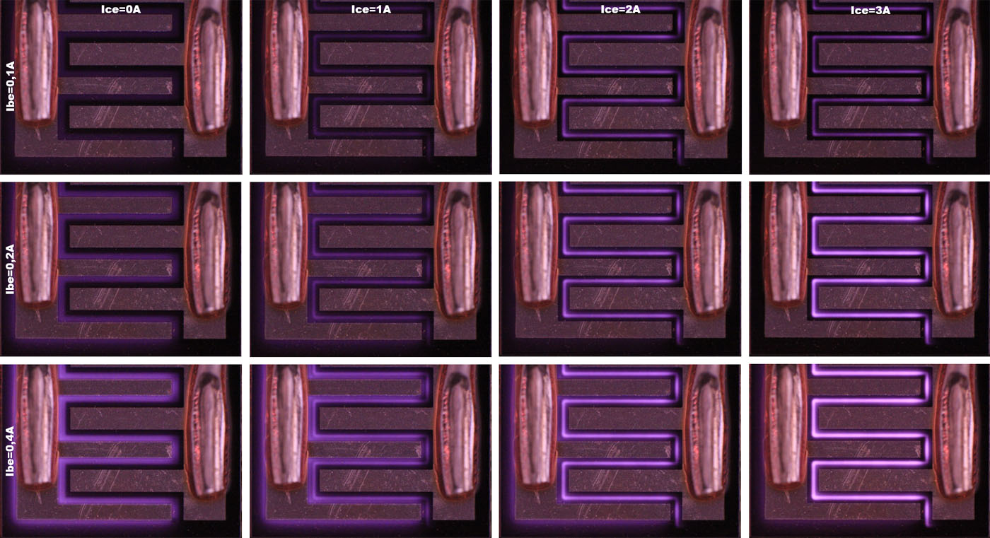
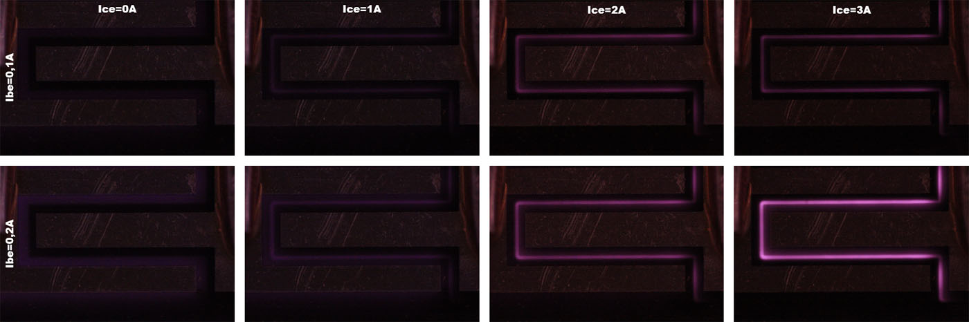
Compared with the SF137 here the base current is on the Y-axis and the collector current is on the X-axis. Without collector current, only the base region is illuminated, below which at the base-collector junction much of the recombination occurs. As the current increases, the light intensity increases.

At high base currents the luminous effect and thus most of the recombination shifts from the base area to the emitter area as the collector current increases. Here, the base current no longer flows via the collector to the emitter, but directly to the emitter in the base layer. At a base current of 0,4A and a collector current of 1A, the separation of base and emitter area can be seen nicely.

At low base currents (0,1A) and high collector currents (3A) the light is concentrated at the edges of the emitter surface. That´s were current crowding takes place, and a large part of the collector-emitter current flows through the edges. The transistor no longer operates in saturation here. In contrast to the SF137, the concentration of the luminance does not increase the brightness.


At a higher magnification, the images appear darker in particular. Otherwise, no other special features can be seen.


https://www.richis-lab.de/BipolarA09.htm#IR

 :-/O
 
The following users thanked this post: SeanB, SilverSolder, RoGeorge

Offline NoopyTopic starter

  • Super Contributor
  • ***
  • Posts: 1734
  • Country: de
    • Richis-Lab
Re: Transistors - die pictures
« Reply #651 on: December 07, 2022, 08:43:29 pm »


Just a small Philips BC548C...
Vce is a little lower than for the BC547C (https://www.richis-lab.de/Bipolar44.htm).


The edge length of the die is 0,32mm. It is thus larger than the die of the BC547, although Vce is lower. Perhaps this is an older design.

The comparison with the PNP transistor BC560 is interesting (https://www.richis-lab.de/Bipolar52.htm). The BC560 used the same design.


https://www.richis-lab.de/BipolarA15.htm

 :-/O
 
The following users thanked this post: SeanB, RoGeorge

Online David Hess

  • Super Contributor
  • ***
  • Posts: 16615
  • Country: us
  • DavidH
Re: Transistors - die pictures
« Reply #652 on: December 08, 2022, 01:58:49 am »
Just a small Philips BC548C...
Vce is a little lower than for the BC547C (https://www.richis-lab.de/Bipolar44.htm).

I always thought these were the same production but graded for Vce.  My own tests with a curve tracer showed that the lower voltage versions often met the higher voltage breakdown specifications.
 

Offline NoopyTopic starter

  • Super Contributor
  • ***
  • Posts: 1734
  • Country: de
    • Richis-Lab
Re: Transistors - die pictures
« Reply #653 on: December 08, 2022, 02:35:10 am »
Just a small Philips BC548C...
Vce is a little lower than for the BC547C (https://www.richis-lab.de/Bipolar44.htm).

I always thought these were the same production but graded for Vce.  My own tests with a curve tracer showed that the lower voltage versions often met the higher voltage breakdown specifications.

Perhaps they are the same production. Since I don't know how old these transistors are it is possible that we look at different generations.

Offline NoopyTopic starter

  • Super Contributor
  • ***
  • Posts: 1734
  • Country: de
    • Richis-Lab
Re: Transistors - die pictures
« Reply #654 on: December 09, 2022, 07:26:49 pm »
I now have a BC section to clear the listing a little: https://www.richis-lab.de/Transistoren_BC.htm


The Philips BC328 is a PNP transistor with a permanent current carrying capacity of 500mA, 1000mA is permissible for a short time. The BC328 blocks up to 25V. The cut-off frequency is 100MHz.


The die with an edge length of 0,57mm corresponds to the design of the MPSA56 (https://www.richis-lab.de/Bipolar38.htm). Compared to other transistors of the BCxxx family, it is relatively large. That is necessary to achieve the specified current carrying capacity. For the same reason, there are relatively large interlocking metal contacts on the die, as we known them from power transistors.


https://www.richis-lab.de/BipolarA16.htm

 :-/O
 
The following users thanked this post: SeanB, RoGeorge

Offline NoopyTopic starter

  • Super Contributor
  • ***
  • Posts: 1734
  • Country: de
    • Richis-Lab
Re: Transistors - die pictures
« Reply #655 on: December 10, 2022, 07:57:04 pm »


The BC338 is the complementary variant of the BC328. The NPN transistor blocks up to 25V, conducts up to 0,5A continuously and 1A for a short time. The cutoff frequency is 100MHz. The current gain factor ranges from 100 to 600.


The edge length of the die is 0,47mm. Thus, it is slightly smaller than the die of the BC328. This is plausible as far as NPN transistors are usually a bit more efficient than PNP transistors.


https://www.richis-lab.de/BipolarA17.htm[/b

 :-/O
 
The following users thanked this post: SeanB, RoGeorge

Offline Sherlock Holmes

  • Frequent Contributor
  • **
  • !
  • Posts: 570
  • Country: us
Re: Transistors - die pictures
« Reply #656 on: December 10, 2022, 10:32:08 pm »
How about a transistor-die-picture-topic?  :)

I have collected some here:

https://www.richis-lab.de/Transistoren.htm


And I just have to show you this one:


You see the breakdown of the KD501-base-emitter-junction with increasing current.  8) ;D


Does anybody know why Tesla integrated this step at the edge of the die?

What truly superb images, absolutely astonishing, keep this up!

“When you have eliminated all which is impossible, then whatever remains, however improbable, must be the truth.” ~ Arthur Conan Doyle, The Case-Book of Sherlock Holmes
 
The following users thanked this post: Noopy

Offline NoopyTopic starter

  • Super Contributor
  • ***
  • Posts: 1734
  • Country: de
    • Richis-Lab
Re: Transistors - die pictures
« Reply #657 on: December 11, 2022, 06:23:33 am »
Thanks!
I still have a big stockpile of pictures and parts too. :-+ 8) As usual: old and new, expensive and low-cost, bulky transistors and tiny complex wonder parts...
 
The following users thanked this post: SeanB, SilverSolder

Offline Kokoriantz

  • Regular Contributor
  • *
  • Posts: 226
  • Country: vn
Re: Transistors - die pictures
« Reply #658 on: December 14, 2022, 03:05:38 am »
Is there a right way to open TO 220 to see the die? I want to compare both Chinese TDA2050 and LM1875.
 

Offline NoopyTopic starter

  • Super Contributor
  • ***
  • Posts: 1734
  • Country: de
    • Richis-Lab
Re: Transistors - die pictures
« Reply #659 on: December 14, 2022, 03:51:05 am »
Is there a right way to open TO 220 to see the die? I want to compare both Chinese TDA2050 and LM1875.

We have discussed how to decap parts in this topic: https://www.eevblog.com/forum/projects/decapping-and-chip-documentation-howto/
And there you can find how I do it.
 
The following users thanked this post: Kokoriantz

Offline NoopyTopic starter

  • Super Contributor
  • ***
  • Posts: 1734
  • Country: de
    • Richis-Lab
Re: Transistors - die pictures
« Reply #660 on: December 18, 2022, 08:09:17 pm »


Another small old Philips transistor. The Philips BC558 PNP transistor has the same datasheet as the BC556. The BC558 is significantly less voltage resistant with 30V, but offers higher amplification factors. In the B variant, the BC556 and BC558 do not differ in this respect. However, the C variant with an amplification factor of 420 to 800 only exists with the BC558. The current carrying capacity is specified with 100mA, 200mA is permissible for a short time. The cutoff frequency is at least 100MHz.


The edge length of the die is 0,32mm. The design can also be found in the PNP transistor BC560C (https://www.richis-lab.de/Bipolar52.htm). The NPN transistor BC548C (https://www.richis-lab.de/BipolarA15.htm) contains these structures too, but the outer metal frame has been omitted.


https://www.richis-lab.de/BipolarA18.htm

 :-/O
 
The following users thanked this post: SeanB, SilverSolder, RoGeorge

Offline NoopyTopic starter

  • Super Contributor
  • ***
  • Posts: 1734
  • Country: de
    • Richis-Lab
Re: Transistors - die pictures
« Reply #661 on: December 20, 2022, 08:01:50 pm »

...


I took some IR pictures of the HFO SL113, this old HF silicon transistor:


In this image a current flows across the base-emitter junction with the collector open. As described with the SF137 (https://www.richis-lab.de/Bipolar75.htm#IR), some light occurs at the base-collector junction. The light is very non-uniform. The upper area remains dark and in the lower area, especially the area under the bondwire is illuminated.


As soon as there is a current flowing through the collector, the light shifts to the emitter area. The light there is somewhat more homogeneous, but still clearly more irregular than for example in the 2N389 (https://www.richis-lab.de/BipolarA09.htm#IR).

The images suggest that either the structures were fabricated irregularly or the areas have such a high resistance that there is no homogeneous current distribution. Since this is a very early silicon power transistor, such deficiencies are hardly surprising.


https://www.richis-lab.de/Bipolar29.htm#IR

 :-/O
 
The following users thanked this post: SeanB, SilverSolder, RoGeorge

Offline NoopyTopic starter

  • Super Contributor
  • ***
  • Posts: 1734
  • Country: de
    • Richis-Lab
Re: Transistors - die pictures
« Reply #662 on: December 28, 2022, 04:19:45 am »


Another old small transistor, a BC547. I don´t know who manufactured it.  :-//


The edge length of the die is 0,32mm. It is thus slightly larger than the Philips version. It is interesting that the outermost metal frame in the area of the base bondpad has been left out.


https://www.richis-lab.de/Bipolar44.htm#unbekannt

 :-/O
 
The following users thanked this post: SeanB, RoGeorge

Offline NoopyTopic starter

  • Super Contributor
  • ***
  • Posts: 1734
  • Country: de
    • Richis-Lab
Re: Transistors - die pictures
« Reply #663 on: December 30, 2022, 07:26:01 pm »


One more small signal transistor. The BC557 is the PNP transistor to the BC547.

I don´t know who manufactured this one but it was in the same circuit as the "unknown" BC547 (https://www.richis-lab.de/Bipolar44.htm).


Hey, that´s the same die as in the BC547!


https://www.richis-lab.de/BipolarA19.htm

 :-/O
 
The following users thanked this post: SeanB, RoGeorge

Offline NoopyTopic starter

  • Super Contributor
  • ***
  • Posts: 1734
  • Country: de
    • Richis-Lab
Re: Transistors - die pictures
« Reply #664 on: January 06, 2023, 08:44:56 pm »
We had the GD609 and the GD619, the complementary Ge transistors with the dendrites in the package:

https://www.richis-lab.de/Bipolar65.htm


The emitter contact was potted with a red silicone now I have removed that stuff.


GD609 - The solder looks a little strange but that´s probably due to the corrosion.


GD619 - The emitter has a strange edged geometry...  ???


https://www.richis-lab.de/Bipolar65.htm#junction

 :-/O
 
The following users thanked this post: SeanB, RoGeorge, Miyuki

Offline NoopyTopic starter

  • Super Contributor
  • ***
  • Posts: 1734
  • Country: de
    • Richis-Lab
Re: Transistors - die pictures
« Reply #665 on: January 13, 2023, 08:07:17 pm »


The  Linear Systems LS5907 is a dual JFET. It is used as an alternative to the TG-168 (https://www.richis-lab.de/K617.htm) in the Keithley 617 electrometer. Linear Systems was founded in California in 1987 and according to their website has acquired processes and products from Amelco, Union Carbide, Intersil and Micro Power Systems.

The LS5907 is part of the LS5905 - LS5909 series. From the LS5906 to the LS5909, the specifications deteriorate, but the LS5905 falls out of line and offers the worst values. For the LS5907, the offset voltage between the two JFETs is a maximum of 5mV. The temperature drift of this voltage is 10µV/°C. The gate current remains below 1pA at 25°C.


This LS5907 was produced in calendar week 12 of 1991.


The potentials of the two JFETs are fed into the package in two groups. Since both JFETs are on the same die, they have very similar temperatures. In addition, production variations affect both transistors very similarly.


The die measures 0,53mm x 0,48mm. The gate potentials frame the corresponding drain and source regions. The upper gate electrodes run between these frames. The reason for the failure is clearly visible. A massive overload has destroyed the gate lead of the right transistor.


https://www.richis-lab.de/FET26.htm

 :-/O
 
The following users thanked this post: SeanB, RoGeorge, 42Khz

Offline NoopyTopic starter

  • Super Contributor
  • ***
  • Posts: 1734
  • Country: de
    • Richis-Lab
Re: Transistors - die pictures
« Reply #666 on: January 15, 2023, 07:55:29 am »


Some more fine Dual-JFETs?
The 2N5905 originally comes from Intersil and belongs to the 2N5902 - 2N5909 series. According to the datasheet, the 2N5905 has a maximum offset voltage of 15mV. The gate current of the 2N5905 is also the highest with a maximum of 3pA at 25°C.


The dual JFET is insulated from the housing with a ceramic plate.


The dimensions of the die are 0,42mm x 0,32mm. The JFET structures are clearly visible. A strip of the metal layer was drawn in between the two transistors.  :-//


https://www.richis-lab.de/FET27.htm

 :-/O
 
The following users thanked this post: SeanB, doktor pyta, RoGeorge

Offline alayn91

  • Newbie
  • Posts: 6
  • Country: fr
Re: Transistors - die pictures
« Reply #667 on: January 15, 2023, 12:56:33 pm »
Hello,
Very interesting discussion.
By any chance, do you have some pictures of the NS LM194/394 ??
If no, could you provide these pictures ?
Thanks in advance.
Alain.


Offline NoopyTopic starter

  • Super Contributor
  • ***
  • Posts: 1734
  • Country: de
    • Richis-Lab
Re: Transistors - die pictures
« Reply #668 on: January 15, 2023, 05:27:23 pm »
I have to take a look into my warehouse, if there is a LM194. If not I can source one.  :-+

Offline magic

  • Super Contributor
  • ***
  • Posts: 6779
  • Country: pl
Re: Transistors - die pictures
« Reply #669 on: January 15, 2023, 08:05:30 pm »
Zeptobars has the LM394. It looks a bit weird.
https://zeptobars.com/en/read/National-LM394CH-super-matched-bjt
 

Offline alayn91

  • Newbie
  • Posts: 6
  • Country: fr
Re: Transistors - die pictures
« Reply #670 on: January 16, 2023, 08:22:58 am »
Hello & thank you !
 

Offline NoopyTopic starter

  • Super Contributor
  • ***
  • Posts: 1734
  • Country: de
    • Richis-Lab
Re: Transistors - die pictures
« Reply #671 on: January 16, 2023, 06:20:48 pm »


Just another 2N590x. The 2N5905 we had yesterday was manufactured by Harris Semiconductor. The 2N5909 shown here was still built by Intersil. Harris Semiconductor took over Intersil in 1988.


The design is basically the same as in the 2N5905, but the ceramic carrier is smaller.


The structures of the JFETs are the same as in the 2N5905. This is not surprising. They are merely different assortments of the same design.


https://www.richis-lab.de/FET28.htm

 :-/O
 
The following users thanked this post: SeanB, SilverSolder, RoGeorge, iMo

Offline NoopyTopic starter

  • Super Contributor
  • ***
  • Posts: 1734
  • Country: de
    • Richis-Lab
Re: Transistors - die pictures
« Reply #672 on: January 18, 2023, 08:48:43 pm »


Does anybody know this logo? It looks like Micro Power Systems. They sold variants of the 2N590x under the names MP590x but their M is different.


Unlike the 2N590x variants from Intersil and Harris Semiconductor the die here is not isolated from the package.


The dimensions of the dies are 0,72mm x 0,66mm. Structures for monitoring the manufacturing process are integrated at the upper edge. The character in the lower right corner, a S or a 5, does not allow us to draw a conclusion about the manufacturer.

An interesting artifact can be found at the right edge. Here, the passivation seems to have delaminated in a small area due to a damage on the edge.


It is immediately noticeable that this are not just two JFETs. Two cascode circuits have been integrated here. The small JFET J1 is the input transistor, while the larger JFET J2 shields the input transistor against the output. This reduces the effective gate drain capacitance.

The gate electrode of J1 is not only shorter, it is also thicker than the gate electrodes of J2. The different geometries are advantageous for the operation of the cascode circuit, in which the upper JFET operates in the linear region while the lower JFET operates in the saturation region.


https://www.richis-lab.de/FET29.htm

 :-/O
 
The following users thanked this post: SeanB, mister_rf, RoGeorge, iMo

Offline mister_rf

  • Contributor
  • Posts: 33
  • Country: ro
Re: Transistors - die pictures
« Reply #673 on: January 18, 2023, 10:04:22 pm »
I have some pics of various 2N2222 transistors produced by different manufacturers.
Here’s the Motorola transistor.
MOTOROLA JAN 2N2222A


« Last Edit: January 18, 2023, 10:05:53 pm by mister_rf »
 
The following users thanked this post: SeanB, exe, RoGeorge

Offline mister_rf

  • Contributor
  • Posts: 33
  • Country: ro
Re: Transistors - die pictures
« Reply #674 on: January 18, 2023, 10:10:47 pm »
CRP INDUSTRIES JAN 2N2222A


The following users thanked this post: SeanB, exe, RoGeorge


Share me

Digg  Facebook  SlashDot  Delicious  Technorati  Twitter  Google  Yahoo
Smf