Author Topic: Transistors - die pictures  (Read 190427 times)

0 Members and 2 Guests are viewing this topic.

Online NoopyTopic starter

  • Super Contributor
  • ***
  • Posts: 1734
  • Country: de
    • Richis-Lab
Re: Transistors - die pictures
« Reply #700 on: May 01, 2023, 08:48:45 pm »
I agree with you.
Thanks for your input.
:-+

Online NoopyTopic starter

  • Super Contributor
  • ***
  • Posts: 1734
  • Country: de
    • Richis-Lab
Re: Transistors - die pictures
« Reply #701 on: May 10, 2023, 06:11:45 pm »


The RCA CA3045 is a transistor array with five transistors. The maximum allowable collector-emitter voltage is at least 15V. Collector currents up to 10mA are specified. By integrating the transistors on one die, the base-emitter voltages differ by a maximum of 5mV, typically just 0,45mV. Typical applications are high frequency applications up to 120MHz.

The transistor array is housed in a somewhat unusual ceramic package with a welded round lid. It allows an operating temperature range of -55°C to 125°C. A sintered ceramic package was also available under the designation CA3045F. An epoxy package was available with the completely different name CA3046. Another variant was the CA3045L, in a so-called beam-lead package that flat terminals can be welded into a circuit.


The datasheet shows the wiring of the transistors. The emitter of transistor Q5 is connected to the substrate. The transistors Q1 and Q2 are connected as a differential amplifiers.


The transistor array is located under the round lid in a round recess.


The die has an edge length of 1,0mm. The round structure on the left edge makes it possible to check the alignment of the masks against each other. 5457 is most likely the internal project designation.

Pin 1 can be identified by the round bondpad. Pin 13, located in the lower left corner, obviously contacts the substrate directly there, as there is no isolation structure under this bondpad.

There are six transistors on the die with the well known standard structure. A C-shaped contact area ties the collector area to a pin. A base area is inserted into the collector area, which in turn contains the emitter area.

The die with the six transistors has been used with different metal layer for different circuits. One variation is the diode array CA3039 with six diodes represented by the base-emitter paths of the transistors (https://www.richis-lab.de/Diode11.htm).


Here you can see another CA3045 transistor array.


The design of the die is very similar to the first transistor array, but there are two small differences. The base wires of the two left transistors in the upper row is not diagonal, but wired in an 90° angle. In addition the 5 in the designation is shifted down a bit.


The manufacturing quality seems a bit worse than on the first CA3045. With a slightly different illumination, scratches can be seen that extend over the entire surface. The scratches are not on the surface or in the metal layer, but are located deeper.

The right edge was either uncleanly separated from the wafer or damaged during installation in the case.


Here you can see another CA3045 with a clearly different housing. The labeling is on the ceramic body. The marking for pin 1 is also printed and not metallized. This is certainly due to the fact that the contacts on the side have no metallization too. The pins are led into the housing.


In this package the design of the second CA3045 can be found. Here, too, the leading 5 of the designation is placed a bit lower.


https://www.richis-lab.de/BipolarA26.htm

 :-/O
 
The following users thanked this post: SeanB, SilverSolder, RoGeorge, ch_scr

Online NoopyTopic starter

  • Super Contributor
  • ***
  • Posts: 1734
  • Country: de
    • Richis-Lab
Re: Transistors - die pictures
« Reply #702 on: May 20, 2023, 05:57:54 pm »


The logo on this power transistor shows that it was manufactured by SGS ATES. However, no information can be found regarding the name IBM458. It can be assumed that this is a transistor that was used in an IBM system. Like Hewlett-Packard, IBM had their own designations printed on their components.


The transistor is located on a round element which was soldered onto a large heatspreader. For contacting the emitter, two bondwires were used and thus the same wire diameter could be used for base and emitter.


The die is protected by a potting material. The black color of the potting material is rather unusual.


The potting is hard to remove, but in the end i managed to clean the die sufficiently.


The edge length of the die is 4,1mm. In the bond area of the emitter, you can see that one of three connections failed. One reason may have been that this contact was largely placed outside the bond area.

As usual, the emitter area is located inside the base area, with both areas interlocking. What is unusual, however, is the additional frame that is connected to the base potential at the associated bondpad. It is routed around the perimeter of the transistor but is isolated from the active base area. It could be that this is a potential steering at the edge. Perhaps there was a danger that the local base potential would become so inhomogeneous due to the current distribution that the transistor would break down at particularly stressful operating points.


There is a round, dark spot in the base bond area for which no explanation can be found.


The base-emitter junction is clearly visible. The additional edges right next to the metal surfaces are most likely the openings through which the metal layer contacts the semiconductor.


https://www.richis-lab.de/BipolarA27.htm

 :-/O
 
The following users thanked this post: SeanB, RoGeorge, ch_scr

Online NoopyTopic starter

  • Super Contributor
  • ***
  • Posts: 1734
  • Country: de
    • Richis-Lab
Re: Transistors - die pictures
« Reply #703 on: May 20, 2023, 05:59:04 pm »


The IBM459 built by SGS ATES is another custom labeled power transistor. No specifications can be found for this component either.


It turns out that the construction is similar to the IBM485. The surfaces show a slightly different color and there is a small blind hole in the base plate of the case underneath the hole in the heatspreader. Also, the bushings for the pins look slightly different. A little less potting was used here, so you can see the edges of the die in the surface.


Optically it is the same transistor as in the IBM485. The additional base ring is slightly wider and the bond area of the emitter is slightly larger. However, this can be explained by different production lines or different revisions of the design.


https://www.richis-lab.de/BipolarA28.htm

 :-/O
 
The following users thanked this post: SeanB, RoGeorge, ch_scr

Online NoopyTopic starter

  • Super Contributor
  • ***
  • Posts: 1734
  • Country: de
    • Richis-Lab
Re: Transistors - die pictures
« Reply #704 on: May 20, 2023, 06:00:20 pm »


The IBM487 is another custom labeled power transistor. No specifications can be found for this component either.


The inside of the transistor appears somewhat discolored. The reason for this could be corrosion effects or a thermal overload. In contrast to the IBM458 and the IBM459, bondwires with different diameters were used here, so that one bondwire was enough for the emitter.


The design is similar to the IBM458 and the IBM459.


https://www.richis-lab.de/BipolarA29.htm

 :-/O
 
The following users thanked this post: SeanB, RoGeorge, ch_scr

Online NoopyTopic starter

  • Super Contributor
  • ***
  • Posts: 1734
  • Country: de
    • Richis-Lab
Re: Transistors - die pictures
« Reply #705 on: May 25, 2023, 06:31:01 pm »


The SMD code J6 stands for the NPN transistor S9014 built by BL Galaxy Electrical. BL Galaxy Electrical is a Chinese manufacturer of less complex semiconductors such as diodes and transistors. The company is part of Changzhou Galaxy Electrical.

The S9014 blocks up to 45V. The maximum collector current is specified as 100mA. With a collector current of 1mA, the current gain may be in a very wide range between 200 and 1000. For this reason, the datasheet specifies two grades. The L category contains the gain factors 200-450 and the H category contains the gain factors 450-1000. The cut-off frequency is 150MHz.


The edge length of the die is just 0,24mm. The emitter surface and the surrounding base contact are clearly visible.


https://www.richis-lab.de/BipolarA30.htm

 :-/O
 
The following users thanked this post: SeanB, RoGeorge, ch_scr

Online NoopyTopic starter

  • Super Contributor
  • ***
  • Posts: 1734
  • Country: de
    • Richis-Lab
Re: Transistors - die pictures
« Reply #706 on: May 28, 2023, 08:14:03 pm »


The SMD code 2A stands for the PNP transistor MMBT3906, which is produced by several manufacturers. The device shown here is from the DT8380 IR thermometer (https://www.richis-lab.de/DT8380.htm). The components used there suggest that in this case the manufacturer is BL Galaxy Electrical.

The MMBT3906 blocks up to 40V. The current carrying capacity is specified as 100mA. With a collector current of 10mA, the current gain is typically 300, but at least 100. The cutoff frequency is at least 250MHz.


The edge length of the die is 0,28mm. The emitter and the surrounding base contact are clearly visible.


The comparison with a CR2032 coin cell and another SOT23 component gives a feeling for the size of the die.


https://www.richis-lab.de/BipolarA31.htm

 :-/O
 
The following users thanked this post: SeanB, exe, RoGeorge

Offline exe

  • Supporter
  • ****
  • Posts: 2562
  • Country: nl
  • self-educated hobbyist
Re: Transistors - die pictures
« Reply #707 on: May 28, 2023, 08:28:57 pm »
Omg, how they cut the waffer? It's like a sand particle.
 

Online NoopyTopic starter

  • Super Contributor
  • ***
  • Posts: 1734
  • Country: de
    • Richis-Lab
Re: Transistors - die pictures
« Reply #708 on: May 28, 2023, 08:36:48 pm »
Think about me peeling this tiny thing out of a black block of burned epoxy.
After that there is some cleaning and putting it in front of the camera in the right direction.  ;D
 
The following users thanked this post: SeanB, SilverSolder, Miyuki

Offline SilverSolder

  • Super Contributor
  • ***
  • Posts: 6126
  • Country: 00
Re: Transistors - die pictures
« Reply #709 on: May 29, 2023, 02:14:38 am »
Think about me peeling this tiny thing out of a black block of burned epoxy.
After that there is some cleaning and putting it in front of the camera in the right direction.  ;D

LOL that makes bulding a ship in a bottle seem like blacksmith work! :D
 

Online NoopyTopic starter

  • Super Contributor
  • ***
  • Posts: 1734
  • Country: de
    • Richis-Lab
Re: Transistors - die pictures
« Reply #710 on: June 06, 2023, 06:25:07 pm »


The SMD code 1AM stands for the bipolar transistor MMBT3904. This transistor is produced by various manufacturers. It remains unclear which manufacturer made this transistor.

The blocking voltage is specified with 40V. The maximum collector current is 200mA constant, 900mA peak. The current gain is typically 300 and the cut-off frequency is at least 300MHz.


The edge length of the die is 0,27mm. This makes the die the same size as most simple small signal transistors. In such transistors, simple designs are usually found in which an emitter area is integrated into a base area. Here, on the other hand, two base areas have been structured, each containing three narrow emitter areas.


https://www.richis-lab.de/BipolarA32.htm

 :-/O
 
The following users thanked this post: SeanB, exe, RoGeorge, bdunham7


Online T3sl4co1l

  • Super Contributor
  • ***
  • Posts: 21684
  • Country: us
  • Expert, Analog Electronics, PCB Layout, EMC
    • Seven Transistor Labs
Re: Transistors - die pictures
« Reply #712 on: June 07, 2023, 01:04:13 am »
Huh, and fT isn't higher? Also their fT curve doesn't meet the minimum? :-DD

...Hmm interesting, few others have a curve but one that does (onsemi) also shows just under 300MHz ...at Vce = 1V?! Weird, go figure. :D

Tim
Seven Transistor Labs, LLC
Electronic design, from concept to prototype.
Bringing a project to life?  Send me a message!
 

Online NoopyTopic starter

  • Super Contributor
  • ***
  • Posts: 1734
  • Country: de
    • Richis-Lab
Re: Transistors - die pictures
« Reply #713 on: June 07, 2023, 03:06:53 am »
Huh, and fT isn't higher? Also their fT curve doesn't meet the minimum? :-DD

...Hmm interesting, few others have a curve but one that does (onsemi) also shows just under 300MHz ...at Vce = 1V?! Weird, go figure. :D

Due to the structures I also expected superior specifications.  :-//
Perhaps they have a worse process (quality) and compensate that with a finer structure because it is easier or cheaper for them.  :-//

Offline bdunham7

  • Super Contributor
  • ***
  • Posts: 7852
  • Country: us
Re: Transistors - die pictures
« Reply #714 on: June 07, 2023, 03:37:27 am »
The edge length of the die is 0,27mm. This makes the die the same size as most simple small signal transistors. In such transistors, simple designs are usually found in which an emitter area is integrated into a base area. Here, on the other hand, two base areas have been structured, each containing three narrow emitter areas.

As always, thank you for posting these.  I'm trying to figure out exactly what each part actually is.  Looking at the second picture, what exactly do the two green squares represent?  Is that the P-type base material?
« Last Edit: June 07, 2023, 03:39:20 am by bdunham7 »
A 3.5 digit 4.5 digit 5 digit 5.5 digit 6.5 digit 7.5 digit DMM is good enough for most people.
 

Online NoopyTopic starter

  • Super Contributor
  • ***
  • Posts: 1734
  • Country: de
    • Richis-Lab
Re: Transistors - die pictures
« Reply #715 on: June 07, 2023, 03:49:11 am »
The edge length of the die is 0,27mm. This makes the die the same size as most simple small signal transistors. In such transistors, simple designs are usually found in which an emitter area is integrated into a base area. Here, on the other hand, two base areas have been structured, each containing three narrow emitter areas.

As always, thank you for posting these.  I'm trying to figure out exactly what each part actually is.  Looking at the second picture, what exactly do the two green squares represent?  Is that the P-type base material?

Yes, the two green squares are base material (p).
In the first picture you can see the narrow red areas that are emitter material (n+).

Online T3sl4co1l

  • Super Contributor
  • ***
  • Posts: 21684
  • Country: us
  • Expert, Analog Electronics, PCB Layout, EMC
    • Seven Transistor Labs
Re: Transistors - die pictures
« Reply #716 on: June 07, 2023, 09:17:59 am »
I wonder what they're doing then... surely not just lower material purity, or sub-par diffusion or epitaxy.  The former would affect hFE at low Ic, and the latter (or both really) would affect Vcbo and Vebo.  Oh hey, I wonder if Vebo is measurable on that yet--?  May be able to get one of your favorite avalanche glow shots.  Although with so little power dissipation of a loose grain-of-sand die, maybe you'll have a hard time getting enough exposure to see it? :-DD  (Nevermind the difficulty probing it, which, I would guess at best might be done with some fiddly cats-whiskers.)

Tim
Seven Transistor Labs, LLC
Electronic design, from concept to prototype.
Bringing a project to life?  Send me a message!
 

Offline exe

  • Supporter
  • ****
  • Posts: 2562
  • Country: nl
  • self-educated hobbyist
Re: Transistors - die pictures
« Reply #717 on: June 07, 2023, 06:56:52 pm »
I don't trust much datasheets for jellybean stuff. I've seen several times that Chinese datasheets are word-by-word copy of other datasheets for stuff like opamps and transistors.

For example, identical datasheets (except logo) from two different vendors:
- https://datasheet.lcsc.com/lcsc/2204201445_HGSEMI-NE5532N_C2987282.pdf
- https://datasheet.lcsc.com/lcsc/2210091830_Slkor-SLKORMICRO-Elec--NE5532S_C5186033.pdf

What makes me very suspicious is that their numbers 1:1 match with TI datasheet: https://datasheet.lcsc.com/lcsc/2005151136_Texas-Instruments-NE5532ADR_C529290.pdf .

An interesting detail: Chinese DS provide phase and gain plots which are not present in others' datasheets. But of poor quality, like a copy of a bad copy. Very suspicious.

Also, I onced got a product change notification from mouser about one jfet. They completely changed device geometry: https://www.mouser.com/PCN/Central_Semiconductor_PCN165_(3).pdf . Later they changed geometry back (though some parameters differ): https://www.mouser.com/PCN/Central_Semiconductor_PCN202.pdf . And it's still the same part number (and perhaps, same number in DS, though I can't find an old revision).  This makes me thinking that datasheets for cheap stuff are pretty "generic".

Your thoughts, gentlemen?
 

Online NoopyTopic starter

  • Super Contributor
  • ***
  • Posts: 1734
  • Country: de
    • Richis-Lab
Re: Transistors - die pictures
« Reply #718 on: June 07, 2023, 07:36:04 pm »
It´s impossible for me to contact this tiny thing of semiconductor! No way!  ;D

And yes, datasheets often lie or don´t tell you everything.
Perhaps this transistor die is much better than a MMBT3904 and they just have put it into a MMBT3904 package because they needed MMBT3904 and had a lot of these dies in stock...  :-//

Online T3sl4co1l

  • Super Contributor
  • ***
  • Posts: 21684
  • Country: us
  • Expert, Analog Electronics, PCB Layout, EMC
    • Seven Transistor Labs
Re: Transistors - die pictures
« Reply #719 on: June 07, 2023, 08:58:30 pm »
Well stuff like 2N3904 are JEDEC registered, so, to the extent JEDEC still controls these parts, they are required to put in those same basic parameters, and meet them.  I don't know what the actual rules if any are, as far as minimum set of parameters, or limitations on additional ones.

Also not sure about variants: MMBT3904 is only a coincidence, not a JEDEC part (well, unless it is, I don't know, but I at least thought the MMBT nomenclature was originally just a Motorola thing).  There are package variants already, like PN2222 vs. 2N2222, or 2N7002 (SOT-23 is used by JEDEC, they're not at all, all THT parts!) vs. 2N7000.

(There's very little JEDEC stuff out there, I imagine partly for historical reasons (much of their work is ancient history at this point) and because of obscurity (mainly semi mfgs really need to know this stuff, as well as actual IP protection / licensing / purchase fees / whatever).  So I don't know a lot of particulars about this, and it doesn't really matter for the most part, assumptions will do well enough.)

Anyway, as far as second-sourcing, the easiest way to sell your parts is to specify them as the originals were specified.  Copy the min/max parameters verbatim, and work to match them as well as is possible (or reasonable).  Maybe lying about some parameters is "okay" (strictly in the business sense, not engineering!), but preferably the typicals are characterized and listed earnestly, and maybe they vary a bit from the originals but for typ that's okay.

Saw one example the other day,
http://file.3peakic.com.cn:8080/product/Datasheet_LM2903A-LM2901A.pdf
Almost certainly a 100% CMOS version, NOT a drop-in equivalent; but looks reasonably useful, and compatible in a lot of applications.  Naming it identically is disingenuous and I'm sure will catch some off guard.

Tim
Seven Transistor Labs, LLC
Electronic design, from concept to prototype.
Bringing a project to life?  Send me a message!
 

Online magic

  • Super Contributor
  • ***
  • Posts: 6779
  • Country: pl
Re: Transistors - die pictures
« Reply #720 on: June 07, 2023, 09:21:57 pm »
What makes me very suspicious is that their numbers 1:1 match with TI datasheet: https://datasheet.lcsc.com/lcsc/2005151136_Texas-Instruments-NE5532ADR_C529290.pdf .

An interesting detail: Chinese DS provide phase and gain plots which are not present in others' datasheets. But of poor quality, like a copy of a bad copy. Very suspicious.
But they don't match the TI datasheet exactly. There are differences such as slew rate and supply current (which also seems specified per channel rather than per package) and errors - their 30nA typical Ibias spec looks unilkely, for example.

The plots are similar to NJM5532 and may have been stolen from there. Plots were also present in Philips, Signetics, Raytheon, possibly others. TI sucks.

I wouldn't trust Chinese datasheets either ;)
 

Online NoopyTopic starter

  • Super Contributor
  • ***
  • Posts: 1734
  • Country: de
    • Richis-Lab
Re: Transistors - die pictures
« Reply #721 on: June 08, 2023, 02:59:43 am »
Anyway, as far as second-sourcing, the easiest way to sell your parts is to specify them as the originals were specified.  Copy the min/max parameters verbatim, and work to match them as well as is possible (or reasonable).  Maybe lying about some parameters is "okay" (strictly in the business sense, not engineering!), but preferably the typicals are characterized and listed earnestly, and maybe they vary a bit from the originals but for typ that's okay.

Saw one example the other day,
http://file.3peakic.com.cn:8080/product/Datasheet_LM2903A-LM2901A.pdf
Almost certainly a 100% CMOS version, NOT a drop-in equivalent; but looks reasonably useful, and compatible in a lot of applications.  Naming it identically is disingenuous and I'm sure will catch some off guard.

I agree with you!  :-+

Online NoopyTopic starter

  • Super Contributor
  • ***
  • Posts: 1734
  • Country: de
    • Richis-Lab
Re: Transistors - die pictures
« Reply #722 on: June 11, 2023, 07:06:58 pm »


The PNP transistor MJ15004 is the complementary type to the MJ15003. The two transistors are optimized for linear operation. The MJ15004 blocks up to 140V and conducts up to 20A (collector) and 25A (emitter) respectively. Up to 250W of power dissipation can be dissipated through the package with its thermal resistance of 0,7°C/W. The cut-off frequency is at least 2MHz. The present model is from Inchange Semiconductor.

I had two components that failed due to oscillations in the same application, a linear regulated power supply.


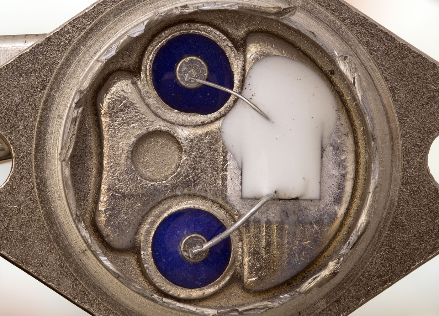
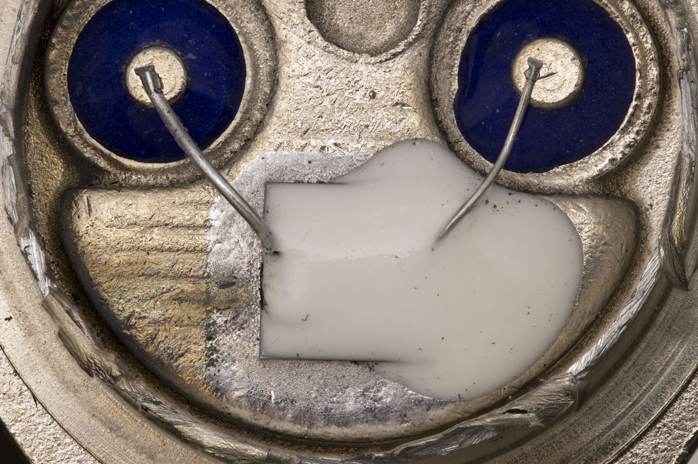
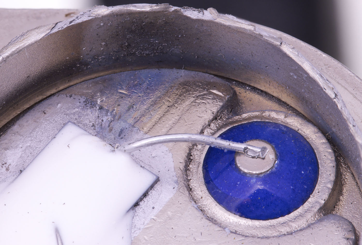
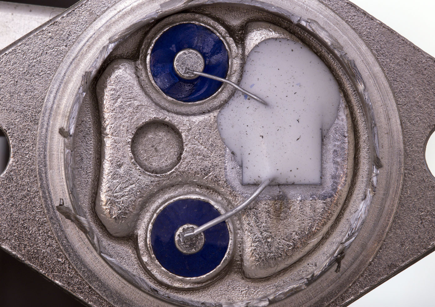
In the case there is a large heatspreader. The die is protected with a white potting, which is often found in Chinese TO packages. The bondwire of the emitter is lager than for the base.


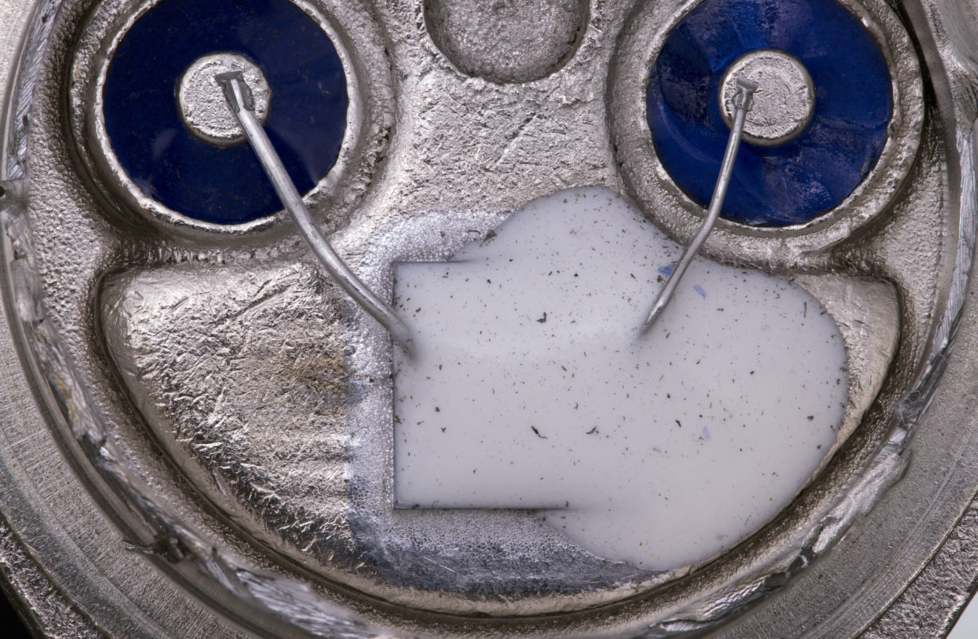
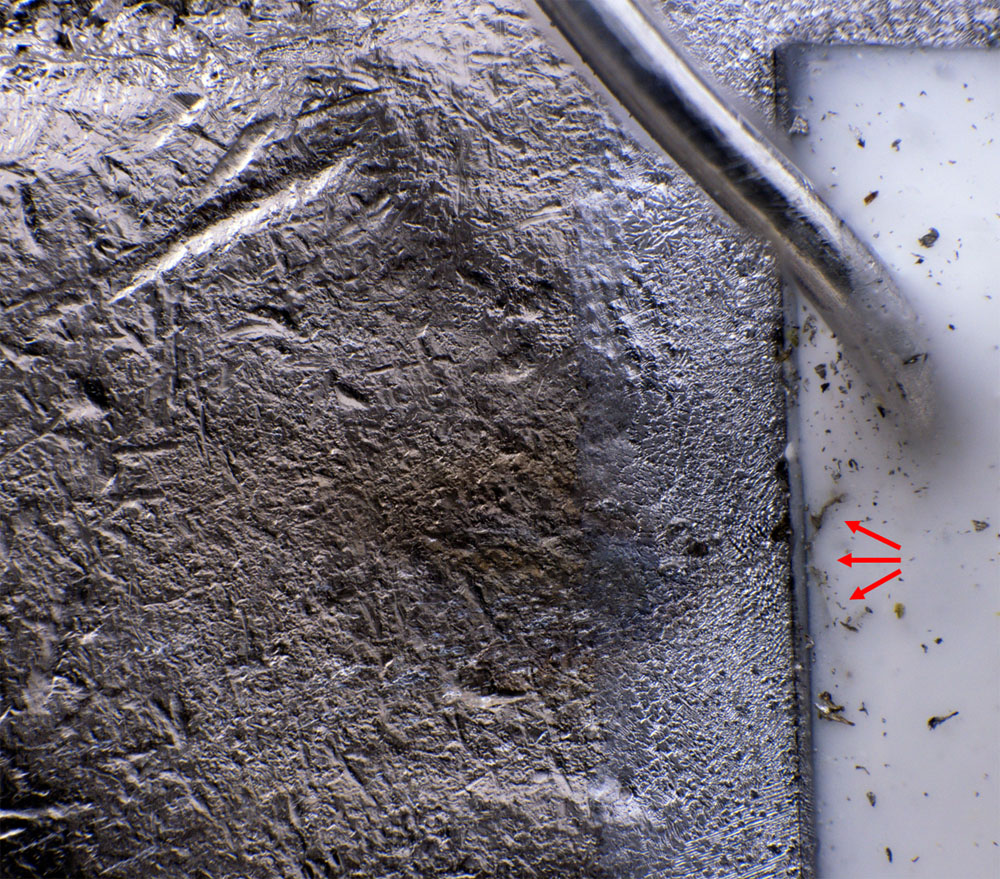
The white potting hides the massive damage to the transistor. A closer look reveals that hot particles have been ejected from the side. These have settled on the heatspreader and the lateral case wall.


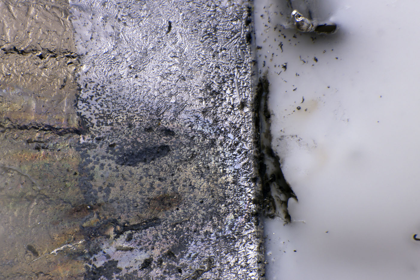
There is a dark rupture on the outer edge of the potting. According to the discolorations on the heatspreader, an arc may have burned there.


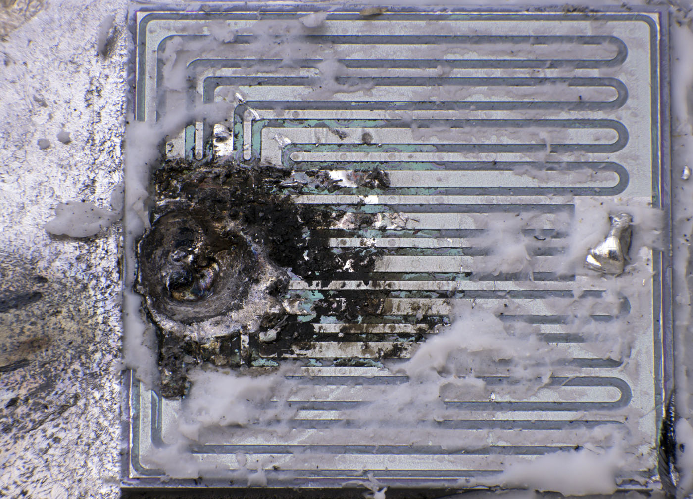
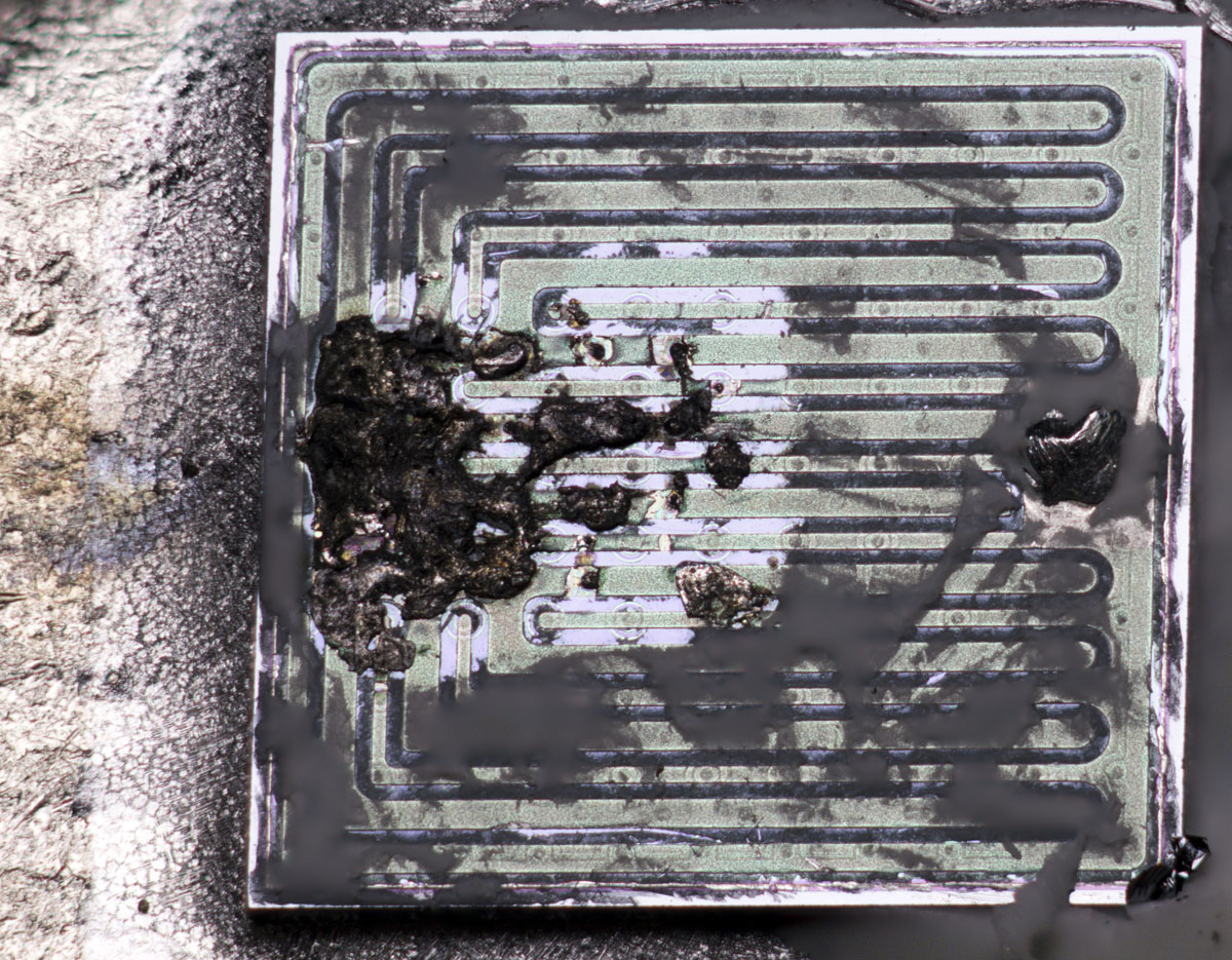
The die has an edge length of 6,1mm. The silicon-like potting is hard to remove. There is a crater where the bondwire contacted the emitter.


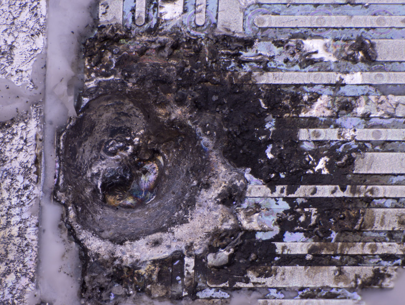
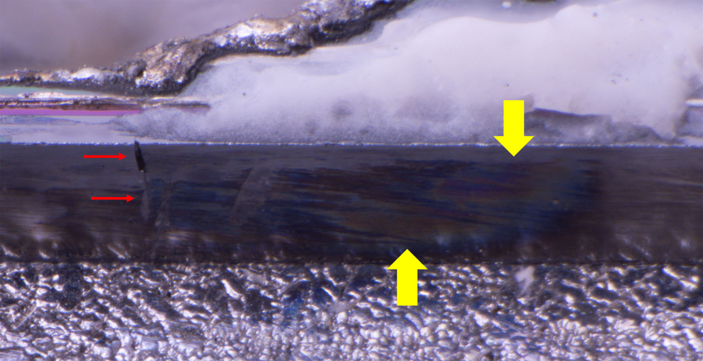
The current flow through the defective transistor has melted a crater into the silicon that extends to the heatspreader.


After further cleaning, it becomes clear that the transistor has a perforated emitter. The emitter completely covers the base and the contacting of the base takes place via round openings in the emitter layer. The large number of distributed base contacts ensures a very low-resistance connection. This allows the free charge carriers to be eliminated more quickly, thus increasing the switching speed. Further advantages are a low saturation voltage, a relatively constant gain factor even with increasing current and a comparatively late onset of avalanche breakdown (second breakdown).

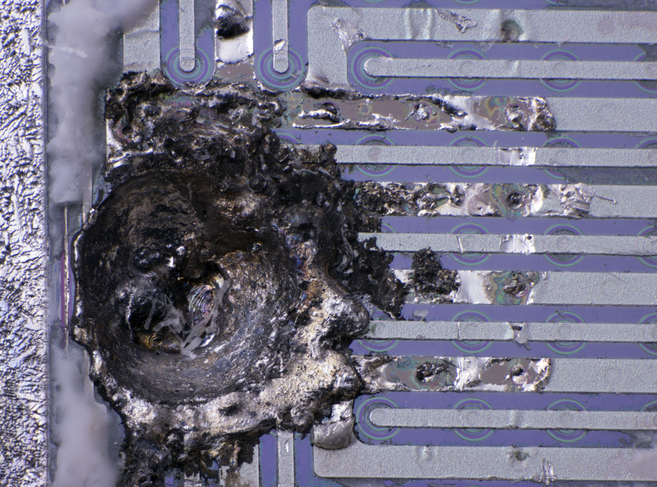
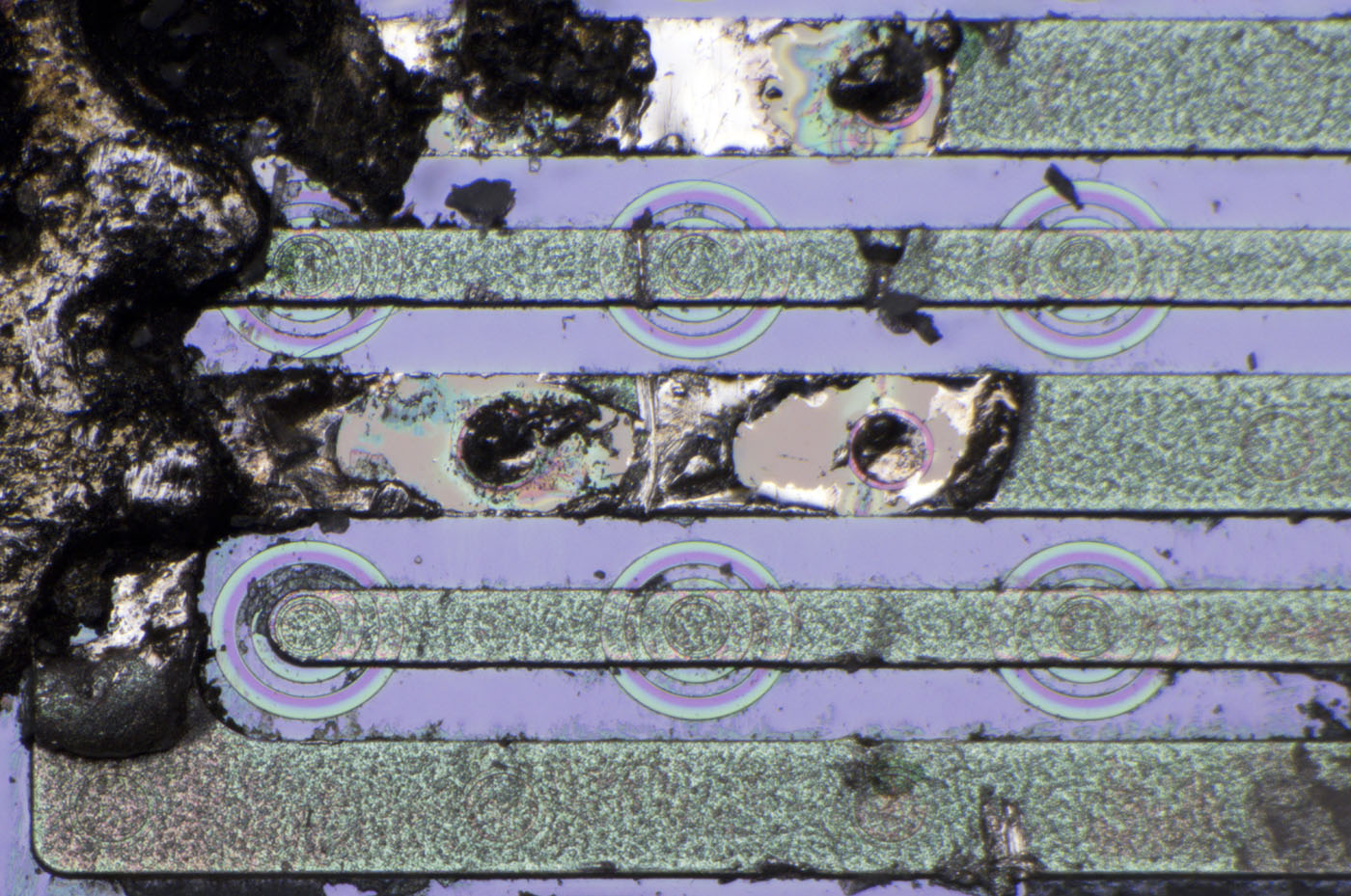
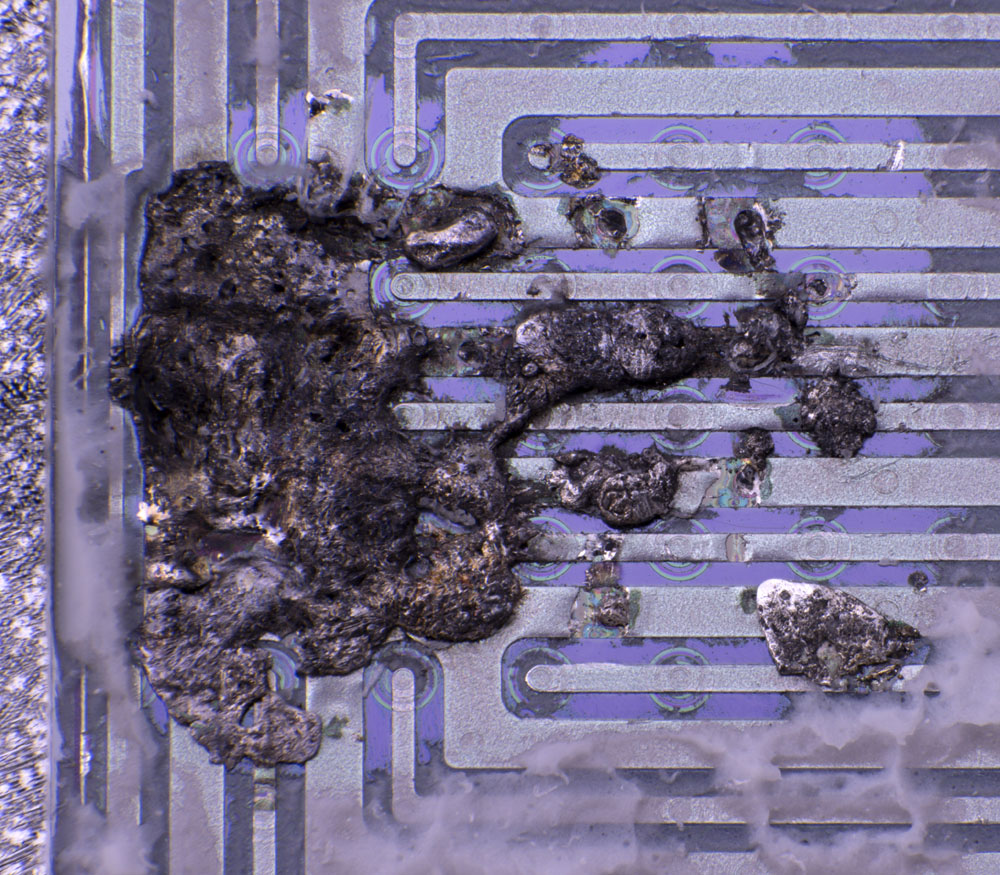
Current flow across the emitter path has melted the metal layer outside the crater. The lower and upper edges of the image show that where the conductor is not completely melted the metal layer in the area of the round contacts has deformed.


As with the BUX22 (https://www.richis-lab.de/Bipolar08.htm) a surprising number of edges are found in the area of the base contacts. One could think that just two rings should be seen, the break-through through the passivation layer and the break-through through the emitter layer. Apparently, the contact areas have a more complex structure. Unfortunately, there is very little information about the exact structure of transistors with perforated emitter.


Discoloration on the side of the die (yellow) shows how high the local heat generation was. This also resulted in the silicon cracking (red).


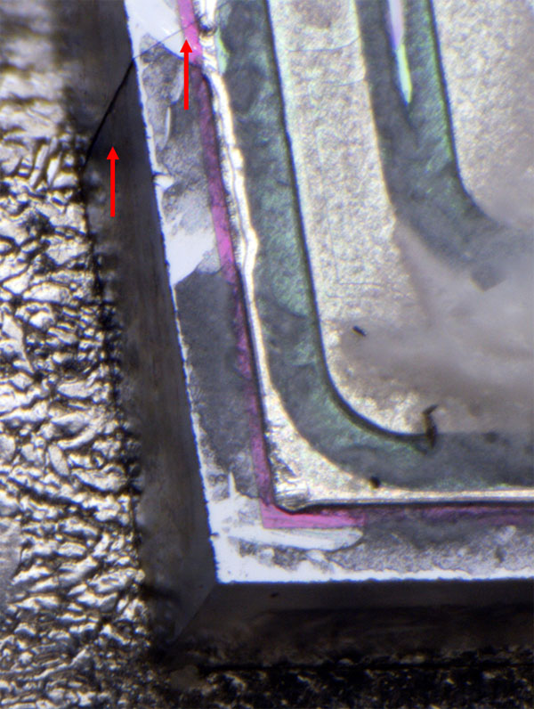
The crack becomes visible one more time in the lower area of the transistor.


The second MJ15004 has an identical design.


Here, too, there is discoloration on the heatspreader in the same area, where hot material has escaped through a crack in the potting (red).


Removing the silicone also reveals massive damage in the contact area of the emitter.


Compared to the upper transistor, the destruction is not as advanced here. The metal layer has melted and the silicon seems to have suffered a bit, but no crater has formed.


https://www.richis-lab.de/BipolarA33.htm

 :-/O
 
The following users thanked this post: SeanB, exe, RoGeorge

Online NoopyTopic starter

  • Super Contributor
  • ***
  • Posts: 1734
  • Country: de
    • Richis-Lab
Re: Transistors - die pictures
« Reply #723 on: June 16, 2023, 07:56:15 pm »


The SCT2450KE is a silicon carbide MOSFET built by Rohm. The transistor blocks up to 1200V and conducts permanently up to 10A. A peak current of 25A is specified. The typical resistance is 450mΩ. Up to 85W can be dissipated through the TO-247 package. The maximum junction temperature is specified as 185°C.

SiC MOSFETs have relatively small output capacitances, allowing low-loss turn-off. For the SCT2450KE, 21pF is specified. The typical turn-off time is 38ns. However, the small capacitances and fast switching increase the risk of high-frequency interference.


The die is covered with a polyimide layer that is difficult to remove. However, the relevant structures can be seen well. The left bondwire carries the source potential, which is distributed to the individual small MOSFET cells via a metal layer. The contacts to these cells are formed in the surface of the metal layer. The right bondwire supplies the gate potential, which is distributed over the right, the upper and the lower side.


The die of the SCT2450KE (1200V / 10A / 0.45Ω) is just 2,0mm x 1,8mm in size. In comparison, the silicon MOSFET STP3NB100FP (https://www.richis-lab.de/FET15.htm / 1000V / 3A / 5.3Ω) is already significantly larger: 3,9mm x 3,7mm, despite its poorer specifications. In contrast, the die of the NDUL09N150C (https://www.richis-lab.de/FET31.htm / 1500V / 9A / 2.2Ω) is once again significantly larger with an edge length of 8mm. Not only is the active area smaller in the SCT2450KE, but the edge structure, which is a potential control, could also be made very slim.


Unlike silicon, silicon carbide is transparent in the visible wavelength range. The metallization on the back of the transistor is chipped off at one point. There you can see the structure of the metallization on the front side through the substrate.


If the upper metal layer is removed with hydrochloric acid, the last coarse impurities disappear.


In detail, you can see the elongated contact from the gate potential to the gate layer that appears pink. From the bondpad, this contact area transitions into the frame structure that distributes the gate potential across the die. The outer frame is again connected to the source potential and provides a uniform potential in the outer area.


Silicon carbide offers a higher dielectric strength than silicon. Accordingly, the SCT2450KE has just a small edge area despite the high reverse voltage of 1000V. A single frame structure was sufficient to control the potential slope.


Viewed from above, the material also appears translucent, but cloudy.


However, if the focal point is chosen differently, it becomes apparent that the material is definitely transparent from above as well.


https://www.richis-lab.de/FET32.htm

 :-/O
 
The following users thanked this post: SeanB, T3sl4co1l, RoGeorge, Miyuki, ch_scr, karpouzi9

Online T3sl4co1l

  • Super Contributor
  • ***
  • Posts: 21684
  • Country: us
  • Expert, Analog Electronics, PCB Layout, EMC
    • Seven Transistor Labs
Re: Transistors - die pictures
« Reply #724 on: June 17, 2023, 06:04:08 am »
Very cool!  AFAIK, SiC are currently not Superjunction, just traditional planar stripe VDMOS or whatever.  The top grid pattern presumably is source connections (vias) dipping down to the die surface, through a grid (square mesh?) of gate connections.  Analogous to ye olde HEXFETs, as far as the top interconnect goes.  But with a square grid, and I assume a vertical trench structure below.  It's not clear if the FET cells would also be on a square grid, or are just stripes the whole width.

The size comparison is particularly apt, as the Si chips are also traditional planar technology -- which puts them at particular disadvantage at the higher voltage ratings.  For that technology, specific Rds(on) scaled something like Vds^2.2.

Thanks to the high breakdown field strength, comparable geometry (e.g. junction depletion widths) would give more like a 100V rating in Si, but more like 1000V in SiC.  That's basically a IRF520!

Oh! I don't suppose that's still working to some extent?  Maybe not after the acid dip, but, I wonder if the body diode glows in forward bias? >:D

Tim
Seven Transistor Labs, LLC
Electronic design, from concept to prototype.
Bringing a project to life?  Send me a message!


Share me

Digg  Facebook  SlashDot  Delicious  Technorati  Twitter  Google  Yahoo
Smf