Author Topic: Voltage regulators - die pictures  (Read 30434 times)

0 Members and 1 Guest are viewing this topic.

Online NoopyTopic starter

  • Super Contributor
  • ***
  • Posts: 1735
  • Country: de
    • Richis-Lab
Re: Voltage regulators - die pictures
« Reply #125 on: March 25, 2023, 04:10:41 pm »
there is no die picture...  ;D

...only "when regulators die" pictures.  8)

Since I'm not a native speaker that should be enough.  :-+ ;D

Offline T3sl4co1l

  • Super Contributor
  • ***
  • Posts: 21688
  • Country: us
  • Expert, Analog Electronics, PCB Layout, EMC
    • Seven Transistor Labs
Re: Voltage regulators - die pictures
« Reply #126 on: March 25, 2023, 06:25:33 pm »
Agree with the failure analysis. :-+

Resistors under the chip, damn, talk about desperate for space! :-DD

Funny enough, I had a similar failure mechanism on an LED lamp I made some years ago.  The main filter cap (47uF 160V I think; 120V single phase only, so this is fine) apparently failed by leakage and corrosion (perhaps it wasn't in great shape to start, perhaps it was installed with too much lead strain; I don't recall it ran hot though), and the failure mechanism leading up to the fault was a noisy and intermittent operation.  The lead corroding off is equivalent to it drying up to ~zero value, and cascading failure ensued (switch avalanche + destruction, controller taken out by backflow from gate pin); and I think that was all that failed, maybe some passives?).  Replaced the relevant parts and good as new, of course.  With a brand new cap (and minimal lead strain) this time. :P

Tim
Seven Transistor Labs, LLC
Electronic design, from concept to prototype.
Bringing a project to life?  Send me a message!
 
The following users thanked this post: Noopy

Offline floobydust

  • Super Contributor
  • ***
  • Posts: 7007
  • Country: ca
Re: Voltage regulators - die pictures
« Reply #127 on: March 25, 2023, 06:28:29 pm »


It appears made by Arch Electronics Taiwan with Traco handling UL certification.
I would make sure the transformer isolation is intact, take it apart like DiodeGoneWild does on his Youtube channel. The DC inductor fail melted turns mean a lot more current than this PSU can put out, came from somewhere.
edit: it's the inductor on the primary-side that fused.

I have found with the Taiwan and china power supply OEM's that they play a game with the quality of the electrolytics. You are given "golden samples" and later the cheap parts come in, and you can't tell because it's all potted. I had some defective due to the transformer being wound incorrectly. It's all good and quiet until you take it apart lol.
« Last Edit: March 25, 2023, 07:11:04 pm by floobydust »
 
The following users thanked this post: SeanB, exe

Offline magic

  • Super Contributor
  • ***
  • Posts: 6779
  • Country: pl
Re: Voltage regulators - die pictures
« Reply #128 on: March 25, 2023, 06:45:18 pm »
The damage of the inductance L1 could be caused by the defect of the switching regulator U1. However, this does not explain the missing capacitance of capacitor C2. It seems most likely that this capacitor was the starting point of the damage. Without sufficient capacitance at the input of the switching regulator, its supply voltage fluctuates very strongly. The inductance L1 can then even generate overvoltages.
U1 and L1 make a nice little boost converter here >:D

...you are right, there is no die picture...  ;D
I counted two ICs on this board, so maybe...
 :popcorn:
 

Online NoopyTopic starter

  • Super Contributor
  • ***
  • Posts: 1735
  • Country: de
    • Richis-Lab
Re: Voltage regulators - die pictures
« Reply #129 on: March 25, 2023, 07:59:01 pm »
It appears made by Arch Electronics Taiwan with Traco handling UL certification.

The Arch power modules look similar. But is there something that makes you sure the TRACO is a Arch module?


I would make sure the transformer isolation is intact, take it apart like DiodeGoneWild does on his Youtube channel. The DC inductor fail melted turns mean a lot more current than this PSU can put out, came from somewhere.
edit: it's the inductor on the primary-side that fused.

I agree with you. I was able to measure a resistance and an inductance but didn´t check it in detail.
My transformer is potted with some hard material. I will try to remove it to take a closer look.


U1 and L1 make a nice little boost converter here >:D

Oh yes...  >:D


I counted two ICs on this board, so maybe...
 :popcorn:

Of course they are in the waiting list.  ;D
Damaged parts can give interesting pictures... ...if they don´t fall apart while decapping.

Offline floobydust

  • Super Contributor
  • ***
  • Posts: 7007
  • Country: ca
Re: Voltage regulators - die pictures
« Reply #130 on: March 25, 2023, 08:15:52 pm »
It appears made by Arch Electronics Taiwan with Traco handling UL certification.
The Arch power modules look similar. But is there something that makes you sure the TRACO is a Arch module?
It's the label on the transformer "ARCH" and the file numbers.
There is no inrush PTC so they must use a very big fuse which can have bad consequences. MST T4A is a slow-blow fuse, 4*In (=16A) 0.15-3 seconds, a bit much for this.
 
The following users thanked this post: Noopy

Online NoopyTopic starter

  • Super Contributor
  • ***
  • Posts: 1735
  • Country: de
    • Richis-Lab
Re: Voltage regulators - die pictures
« Reply #131 on: March 25, 2023, 08:29:06 pm »
Indeed, I didn´t see the "ARCH-E" on the transformer.  :-+

Yes, it´s really a big fuse for that small power module.

Offline AnalogTodd

  • Regular Contributor
  • *
  • Posts: 89
  • Country: us
Re: Voltage regulators - die pictures
« Reply #132 on: March 25, 2023, 09:30:36 pm »
Just found this thread. Think I'll have to keep an eye on it, considering it covers the job I did for a lot of years...
Lived in the home of the gurus for many years.
 

Online NoopyTopic starter

  • Super Contributor
  • ***
  • Posts: 1735
  • Country: de
    • Richis-Lab
Re: Voltage regulators - die pictures
« Reply #133 on: March 25, 2023, 09:49:51 pm »
Just found this thread. Think I'll have to keep an eye on it, considering it covers the job I did for a lot of years...

If you are interested in more die pictures just look at my other topics...

Offline AnalogTodd

  • Regular Contributor
  • *
  • Posts: 89
  • Country: us
Re: Voltage regulators - die pictures
« Reply #134 on: March 25, 2023, 10:01:15 pm »
I've looked through those as well. To me, the voltage regulators is a special one since that was what I designed for a lot of years.
Lived in the home of the gurus for many years.
 

Offline exe

  • Supporter
  • ****
  • Posts: 2563
  • Country: nl
  • self-educated hobbyist
Re: Voltage regulators - die pictures
« Reply #135 on: March 26, 2023, 06:03:54 am »
I've looked through those as well. To me, the voltage regulators is a special one since that was what I designed for a lot of years.

Can you disclose which regulators you designed?
 

Offline AnalogTodd

  • Regular Contributor
  • *
  • Posts: 89
  • Country: us
Re: Voltage regulators - die pictures
« Reply #136 on: March 26, 2023, 02:37:10 pm »
A good portion of the LTC portfolio is mine. All of the LT176X linear regulators, LT3080 family, LT3093, LT3094, and others.
« Last Edit: March 26, 2023, 02:39:01 pm by AnalogTodd »
Lived in the home of the gurus for many years.
 
The following users thanked this post: exe, RoGeorge, Zoli

Offline magic

  • Super Contributor
  • ***
  • Posts: 6779
  • Country: pl
Re: Voltage regulators - die pictures
« Reply #137 on: March 26, 2023, 08:27:33 pm »
That's some good stuff :-+
(Still curious how those precision rail-to-rail current sources work...)
 

Offline AnalogTodd

  • Regular Contributor
  • *
  • Posts: 89
  • Country: us
Re: Voltage regulators - die pictures
« Reply #138 on: March 26, 2023, 09:52:25 pm »
Smoke and mirrors. Which is why they stop working when someone lets the smoke out...

Technically, what we do is create a voltage that has a flat characteristic across temperature and drop it across a resistor. Set things up right and it only takes a couple hundred millivolts of headroom to run from the rail (though the bulk of the circuit takes a couple volts to run from VIN to GND).
Lived in the home of the gurus for many years.
 

Offline exe

  • Supporter
  • ****
  • Posts: 2563
  • Country: nl
  • self-educated hobbyist
Re: Voltage regulators - die pictures
« Reply #139 on: March 27, 2023, 06:37:36 pm »
LT3080 family

Oh, those are my favorite)
 

Offline AnalogTodd

  • Regular Contributor
  • *
  • Posts: 89
  • Country: us
Re: Voltage regulators - die pictures
« Reply #140 on: March 28, 2023, 07:58:20 pm »
The Linear Technology LT3750...


We had this strange NPN transistors in the LT3750.


I found a good explanation for these structures in the book "The Art of Analog Layout" by Alan Hastings.

The basis is a so-called CDI bipolar transistor, as it is common in a BiCMOS process. CDI stands for "collector diffused isolation" and describes the isolation of the transistor from its environment by an n-doped well within the p-doped epitaxial layer. The special feature is the emitter, which is created by applying a heavily n-doped polysilicon layer over an oxide mask and allowing its doping to diffuse into the base surface.

A transistor constructed in this way has a small emitter with high doping. The base area can also be made more highly doped and thinner. All this has a positive effect on the transistor's properties. Current gain and switching frequency are very high.

Consequently, the dark areas of the transistors are the openings where the red polysilicon layer forms the emitter surfaces. Whether this is really a BiCMOS process remains questionable, since no MOSFETs can be seen in the whole circuit. Nevertheless, the emitters can be represented by a polysilicon layer.


https://www.richis-lab.de/voltageregulator18.htm#Poly-Emitter

 :-/O
That is a correct description of these devices. The interesting bit is when you look at some of them where the contact is directly over the emitter, but there are others where it appears contacts are not over the emitters. This was done to promote matching of devices; a contact directly in the emitter region could cause defects that contributed to mismatch, but use the conductive poly to bring the emitter connection out and away and you get better results.
Lived in the home of the gurus for many years.
 
The following users thanked this post: SeanB, RoGeorge, floobydust, Noopy

Online NoopyTopic starter

  • Super Contributor
  • ***
  • Posts: 1735
  • Country: de
    • Richis-Lab
Re: Voltage regulators - die pictures
« Reply #141 on: March 28, 2023, 08:00:12 pm »
Very interesting! Thanks for providing this information!  :-+

Online NoopyTopic starter

  • Super Contributor
  • ***
  • Posts: 1735
  • Country: de
    • Richis-Lab
Re: Voltage regulators - die pictures
« Reply #142 on: May 30, 2023, 06:50:50 pm »


The Taiwanese company Holtek is best known for its microcontrollers. Holtek works fabless. This means that they do not have any production lines themselves. Holtek develops circuits and then has them produced by contract manufacturers (foundries) such as TSMC.

The HT7530-1 is a 3V voltage regulator that can deliver up to 100mA. The SOT89 package allows a power dissipation of up to half a watt. The maximum allowable input voltage is 30V. Without any load the HT7530 draws just 2,5µA. 15 alternative variants of the voltage regulator provide surprisingly finely graded output voltages between 2,1V and 15V. The initial accuracy is +/-3%. The temperature drift is given as 100ppm/°C. As a low-drop voltage regulator, the minimum required voltage drop across the device is typically just 30mV (at 1mA).


The datasheet describes that the HT7530 is based on a CMOS process. A relatively simple block diagram is also shown there.


The dimensions of the die are 0,46mm x 0,41mm. Although the structures are very small, you can still make out the functional blocks. The large evenly structured area contains the power transistor. As usual for a power MOSFET, the transistor consists of many small cells. Accordingly, the bondpads in the upper corners must be the input and the output of the regulator. Thus, the lower bondpad on the left edge must be the contact for the reference potential.

In the lower area, five testpads are placed, between which you can make out fuses. Below the testpads, a whole row of resistors extend from the left to the right edge. On the right edge there is another testpad that seems to operate a fifth fuse in the lower area. Either the output voltage is adjusted with these structures or the voltage regulator can initially display all output voltages listed in the datasheet and one of them is selected via the testpads. The relatively high tolerance of +/-3% speaks for the second possibility. Due to the partly small gradations of the possible output voltages, it is possible that both a selection of the output voltage and a certain adjustment is possible via the fuses.

The rest of the circuit is between the power transistor and the testpads. In fact, it seems to be only a few elements. In this case, the block diagram is probably not oversimplified.


https://www.richis-lab.de/voltageregulator21.htm

 :-/O
 
The following users thanked this post: SeanB, exe, RoGeorge, floobydust, MegaVolt

Online NoopyTopic starter

  • Super Contributor
  • ***
  • Posts: 1735
  • Country: de
    • Richis-Lab
Re: Voltage regulators - die pictures
« Reply #143 on: November 17, 2023, 08:26:17 pm »


The LM125 is a voltage regulator with two output voltages, +15V and -15V. In addition to the LM125, which is specified for an operating temperature range of -55°C to 125°C, National Semiconductor also sold the LM325, which is specified to operate between 0°C and 70°C. The same datasheet also includes the LM126 and LM326, which supply output voltages of -12V and 12V. The maximum input voltage is +/-30V. The maximum output current is 100mA. Overcurrent protection typically kicks in at 260mA.


The circuit diagram in the datasheet is rather confusing at first glance.


In contrast, the description of the LM125 in Application Note 82 from National Semiconductor is much easier to understand and very detailed (https://www.richis-lab.de/images/vreg/24x05.pdf). The block diagram you see here provides an overview. The reference voltage is generated on the negative side. The resistors Ra and Rb define the output voltage. The positive voltage regulator uses the negative output voltage as a reference. If the negative voltage rises, the positive voltage falls accordingly. For this reason, the LM125 is also referred to as a "tracking regulator". The resistors Rc and Rd define the output voltage on the positive side.


The dimensions of the die are 2,3mm x 1,6mm. The large output stage transistors are clearly visible on the right and left edges. Some resistors with additional contacts have been integrated in the center of the die. These are probably the feedback resistors Ra to Rd and the additional contacts make it possible to switch from 15V to 12V with a simple change of the metal layer.


https://www.richis-lab.de/voltageregulator22.htm

 :-/O
 
The following users thanked this post: SeanB, RoGeorge

Online NoopyTopic starter

  • Super Contributor
  • ***
  • Posts: 1735
  • Country: de
    • Richis-Lab
Re: Voltage regulators - die pictures
« Reply #144 on: January 08, 2024, 04:40:15 am »


The SG3532 voltage regulator is very similar to the LM723 (https://www.richis-lab.de/LM723.htm). Silicon General advertises the wider operating voltage range, which extends from 4,5V to 50V. In addition, there is overcurrent protection in the power path and at the reference output, overtemperature protection and a pin with which the voltage regulator can be deactivated. The SG3532 allows an output current of up to 250mA.

Only the SG1532 and SG2532 variants allow the full 50V. The SG3532 is only approved for 40V. These appear to be different bins. The SG1532 also offers an extended operating temperature range of -55°C to 125°C.


The circuit diagram in the datasheet shows a similar, but slightly different circuit compared to the LM723. The SG3532 uses a bandgap reference.


The dimensions of the die are 1,7mm x 1,5mm. The letters CG in the upper left corner could be the initials of a developer. The numbers 1532 stand for the variant SG1532.


The datasheet contains an illustration of the metal layer. This shows that the layout has been revised at least once. The structure is apparently basically the same, but some structures have changed in the left-hand area.


Test structures of eight masks are shown in the bottom left-hand corner, which allow the exposure performance of the process to be evaluated.


https://www.richis-lab.de/voltageregulator23.htm

 :-/O
 
The following users thanked this post: SeanB, RoGeorge, ch_scr, D Straney

Online NoopyTopic starter

  • Super Contributor
  • ***
  • Posts: 1735
  • Country: de
    • Richis-Lab
Re: Voltage regulators - die pictures
« Reply #145 on: January 10, 2024, 07:27:27 pm »


I have taken a closer look at the circuit. You can see that it largely corresponds to the circuit in the datasheet. Some resistors, mainly emitter resistors, have not been included and the bias circuit is slightly different. An additional transistor has been integrated at the current mirror around Q15, which supplies the base currents for the current sources. The current mirror around Q22 is also somewhat more complex.

Two bondpads are provided for the shutdown pin, as it is led out at a different point in the TO package than in the DIL package. The capacitor C1 uses two capacitances. Under the upper electrode, built in the metal layer, the barrier layer of a base-emitter structure provides an additional high capacitance. The transistor Q29 has an unusual structure. The area between the base and collector has been enlarged and structured so that an additional capacitance is created there.


Now let´s take a second look at the metal layer in the datasheet. Presumably it is the current sources that have been revised and no longer fully correspond to the circuit diagram. The overcurrent protection with Q29 does not seem to have had any capacity in this revision.


https://www.richis-lab.de/voltageregulator23.htm#schematic

 :-/O
 
The following users thanked this post: SeanB, RoGeorge, ch_scr

Online NoopyTopic starter

  • Super Contributor
  • ***
  • Posts: 1735
  • Country: de
    • Richis-Lab
Re: Voltage regulators - die pictures
« Reply #146 on: February 18, 2024, 05:32:20 am »


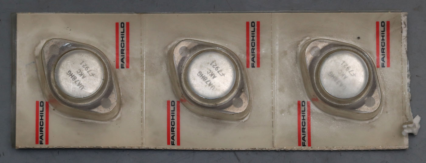
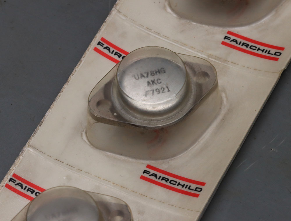
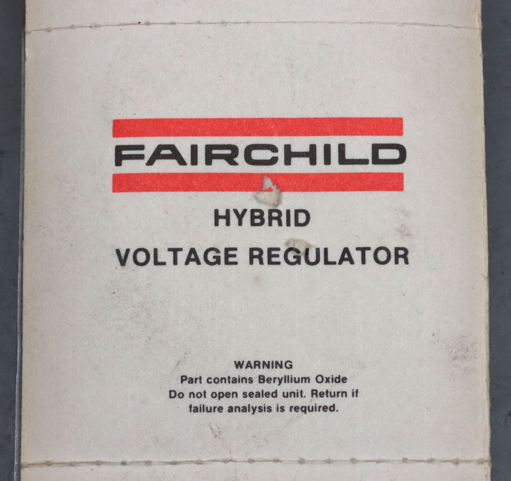
The Fairchild µA78HG voltage regulator is shown here in the original packaging. The H in the designation shows that it is a hybrid component. There is a note on the back that the package contains beryllium oxide and that the voltage regulator should therefore be returned to Fairchild for fault analysis.

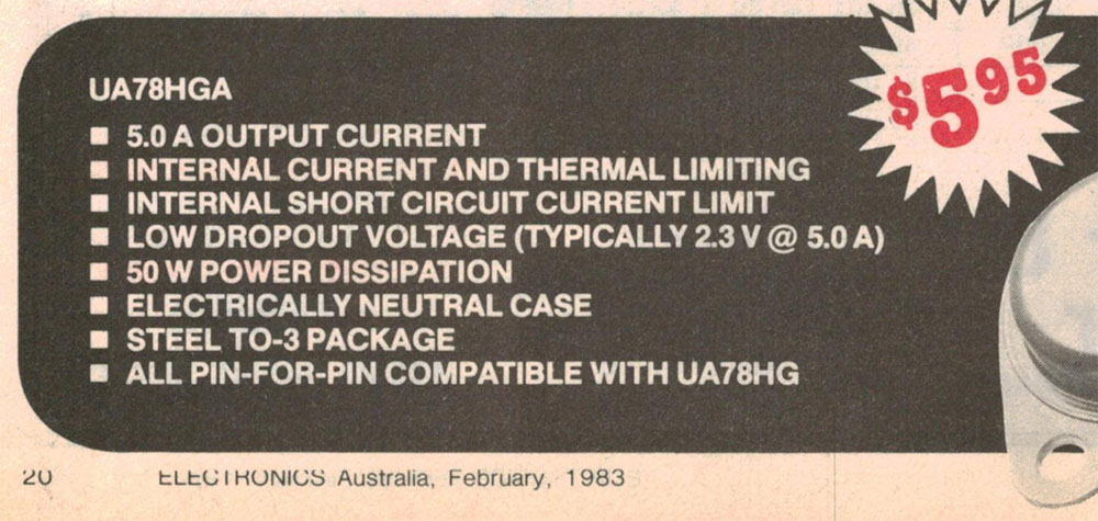
With an input voltage of up to 40V, the output voltage of the µA78HG can be set between 5V and 24V via a voltage divider. The output current is specified with a maximum of 5A. The short-circuit protection typically kicks in at 7A. Up to 50W can be dissipated.


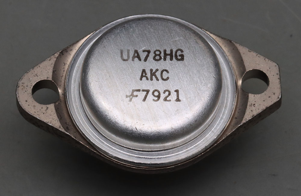
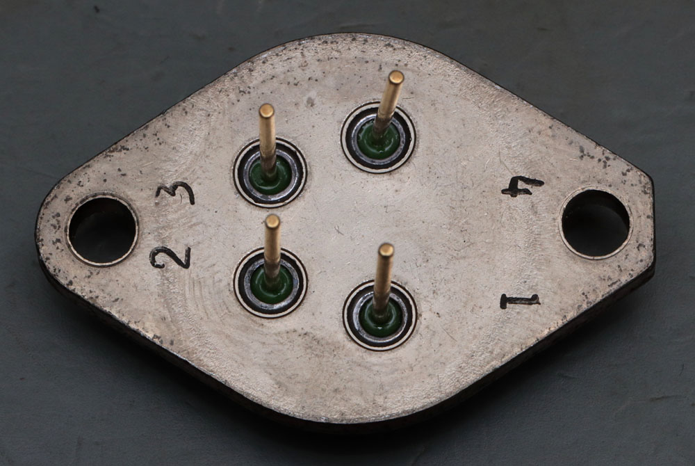
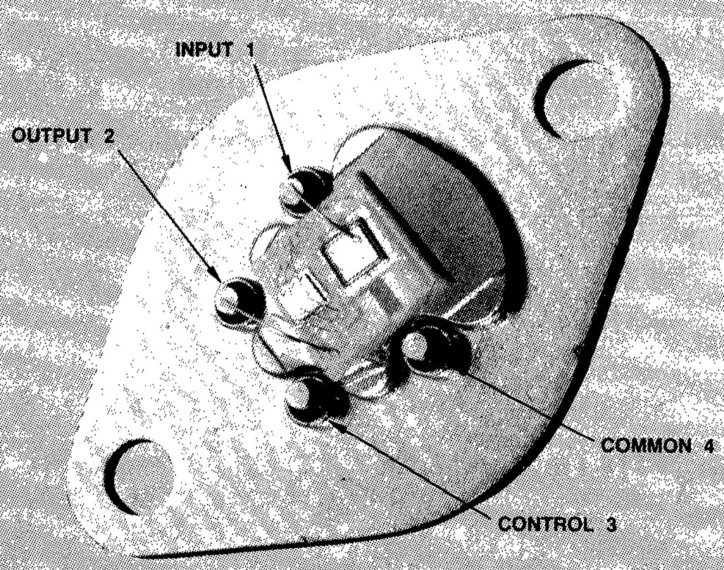
The µA78HG is housed in a TO-3 package. This is the historical widespread variant with a very thick base plate. As the component has four potentials to the outside, the TO-3 variant with four pins was selected. Numbers help to identify the pins. The base plate is flattened on one side so it´s easier to mount the regulator in the right orientation.


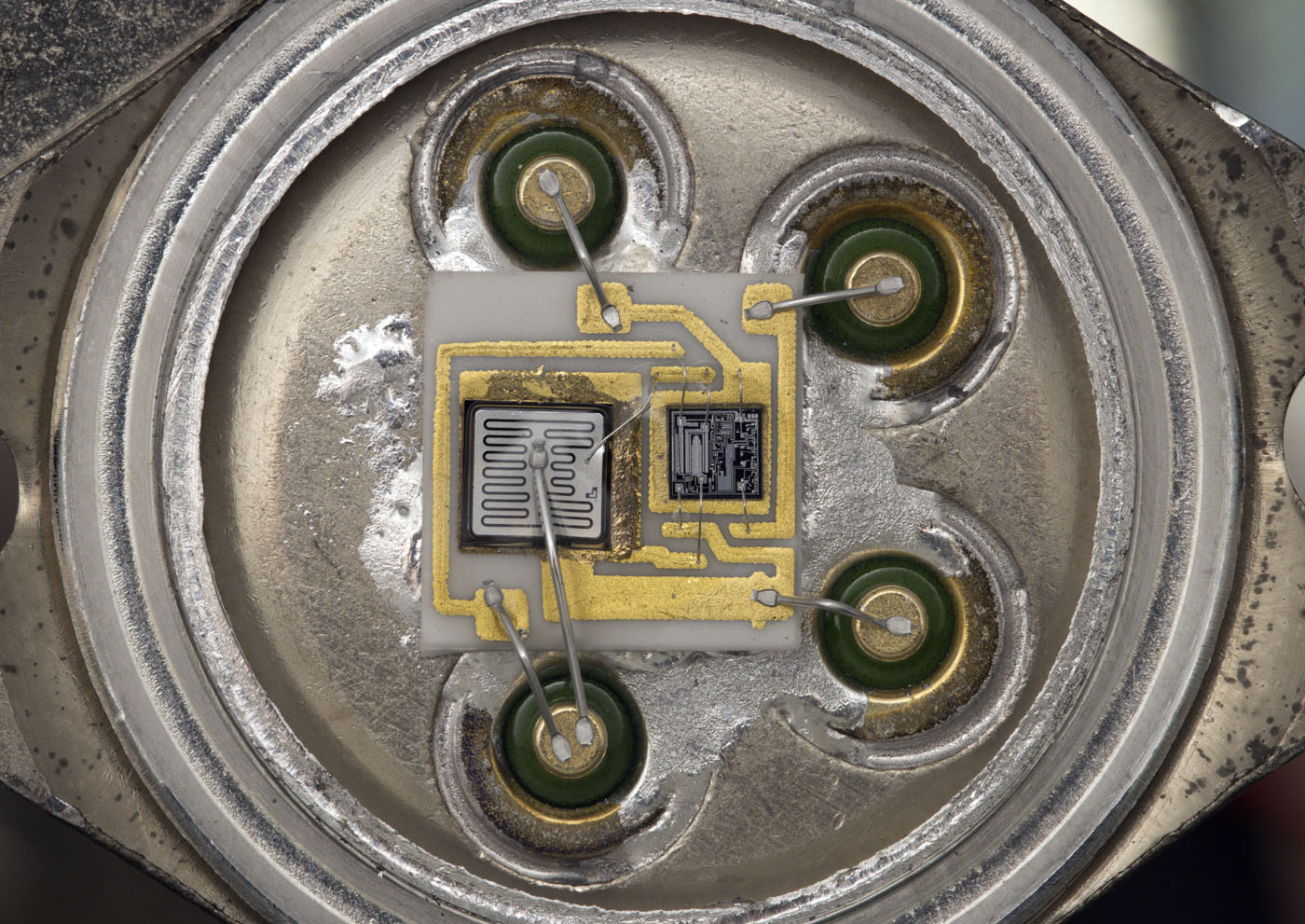
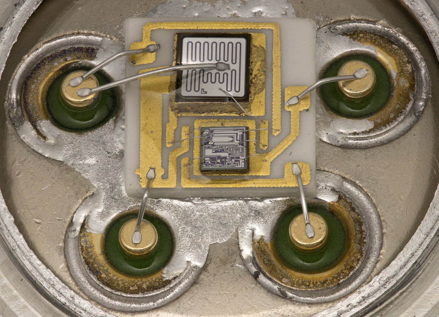
The housing contains a ceramic carrier on which an integrated circuit and a power transistor are placed. A clear encapsulation protects the semiconductors.


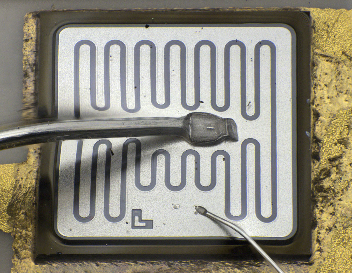
The transistor has a MESA structure. The edge length is 3,0 mm. The thick bondwire conducts the supply potential coming from the left hand side. The base area is contacted with a thin bondwire. The fact that the supply potential contacts the emitter area shows that it is a PNP transistor.


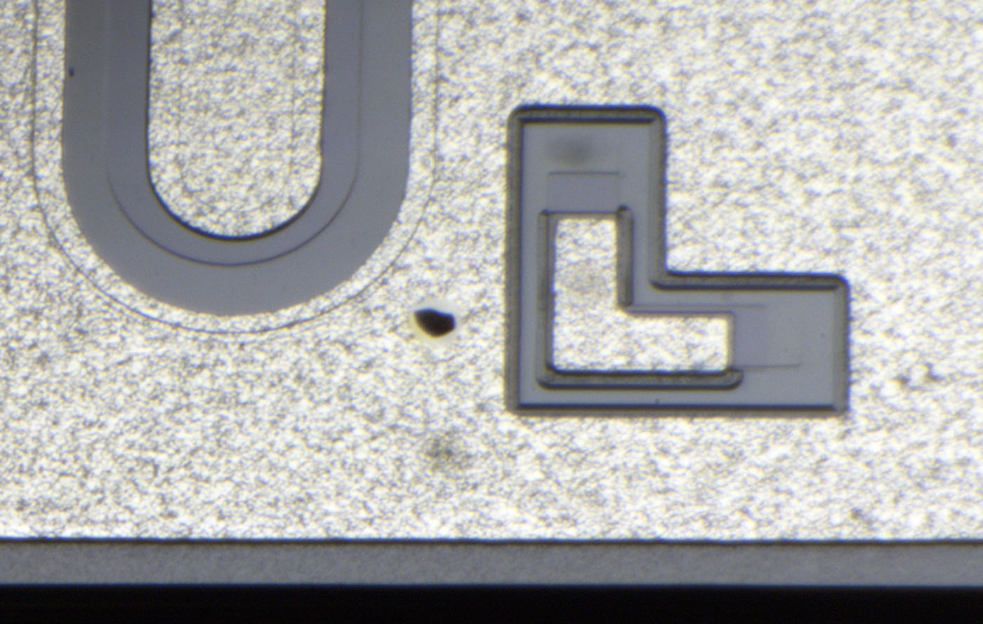
There is an L-shaped structure on the lower edge. This can be used to check how well the masks were aligned during production.


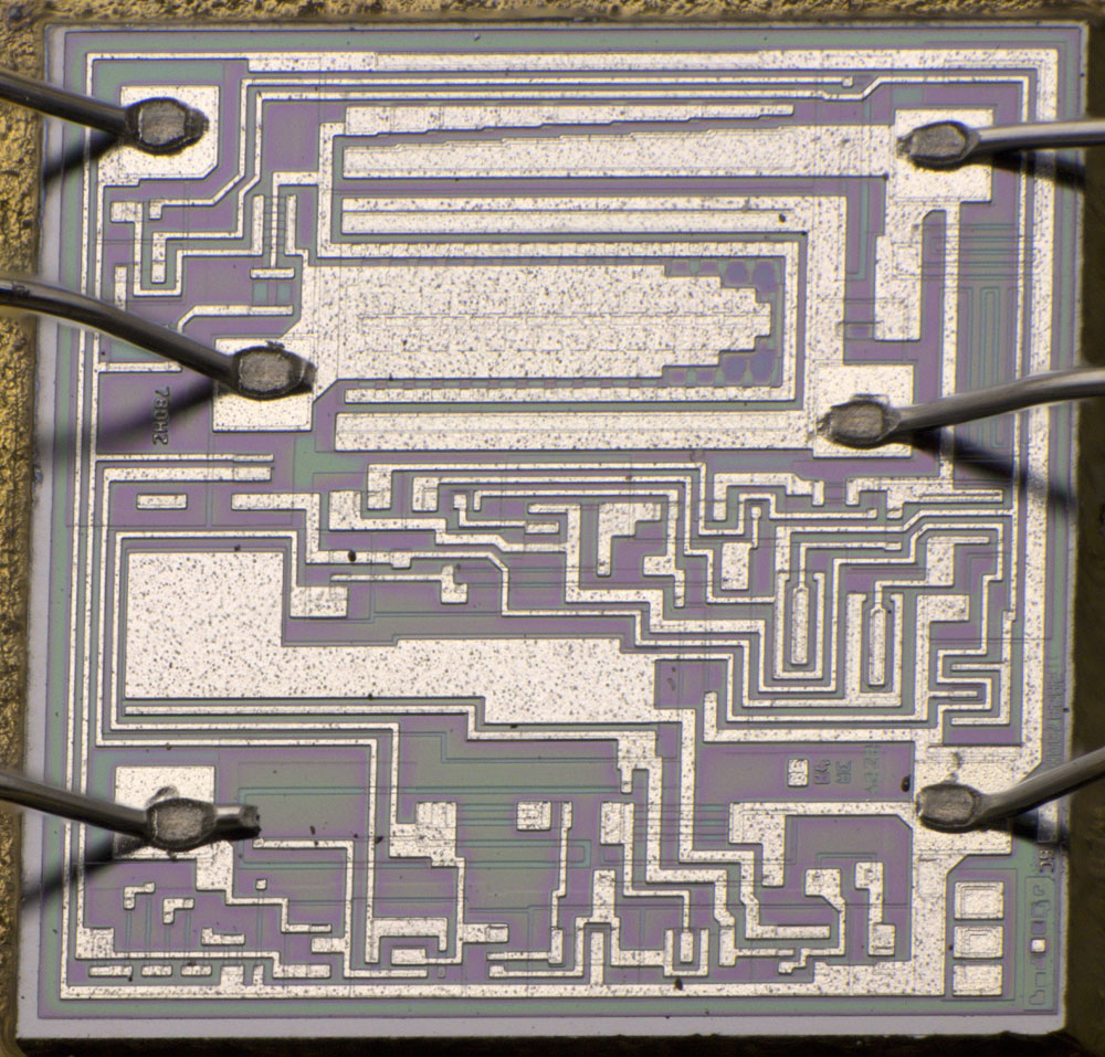
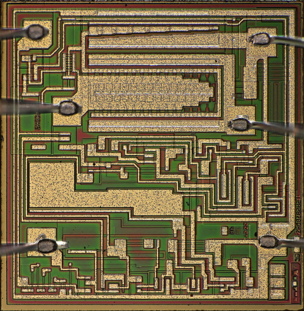
The integrated circuit contains the regulator. The dimensions of the die are 1,8mm x 1,9mm.


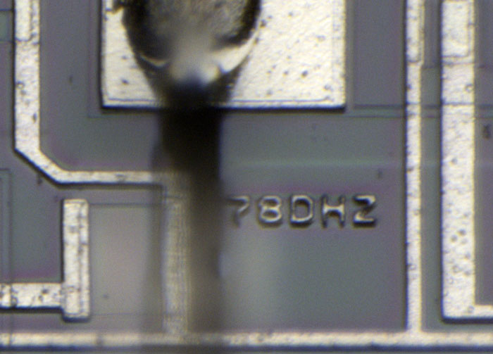
The designation 78DHZ is shown in the metal layer on the left side of the die.


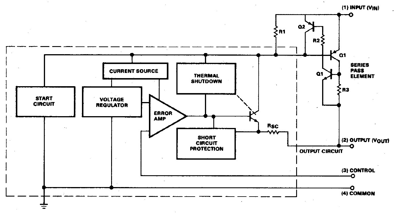
The Fairchild Voltage Regulator Handbook from 1978 contains a block diagram for the µA78HG. The integrated part is labelled as µA78M00. The µA78M00 itself is already a complete voltage regulator. The external elements merely extend the current carrying capability and realise overcurrent protection in this path.

As will be shown later, the representation of the external component does not match the µA78HG documented here. The series regulator transistor and its shunt are actually external. However, the µA78M00 is responsible for detecting and switching off the overcurrent. For this just a small modification of the metal layer was necessary. Perhaps there was an earlier revision in which the µA78M00 regulator was an unmodified voltage regulator and all the elements seen here had to be integrated externally.


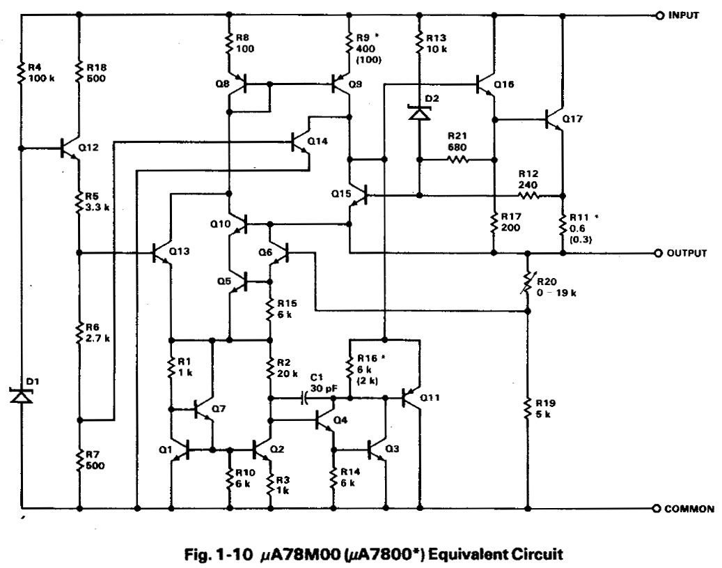
A detailed circuit diagram of the µA78M00 is also documented in the Fairchild Voltage Regulator Handbook. The Siemens TDB7805 has the same structure. The functionality of the circuit is described there in more detail (https://www.richis-lab.de/voltageregulator05.htm). However, here a fixed-voltage version without the modification for use with an external series regulator is shown. A µA78M05 with an output voltage of 5V would look like this, for example. The voltage divider for the feedback is integrated in these regulators (R19/R20).


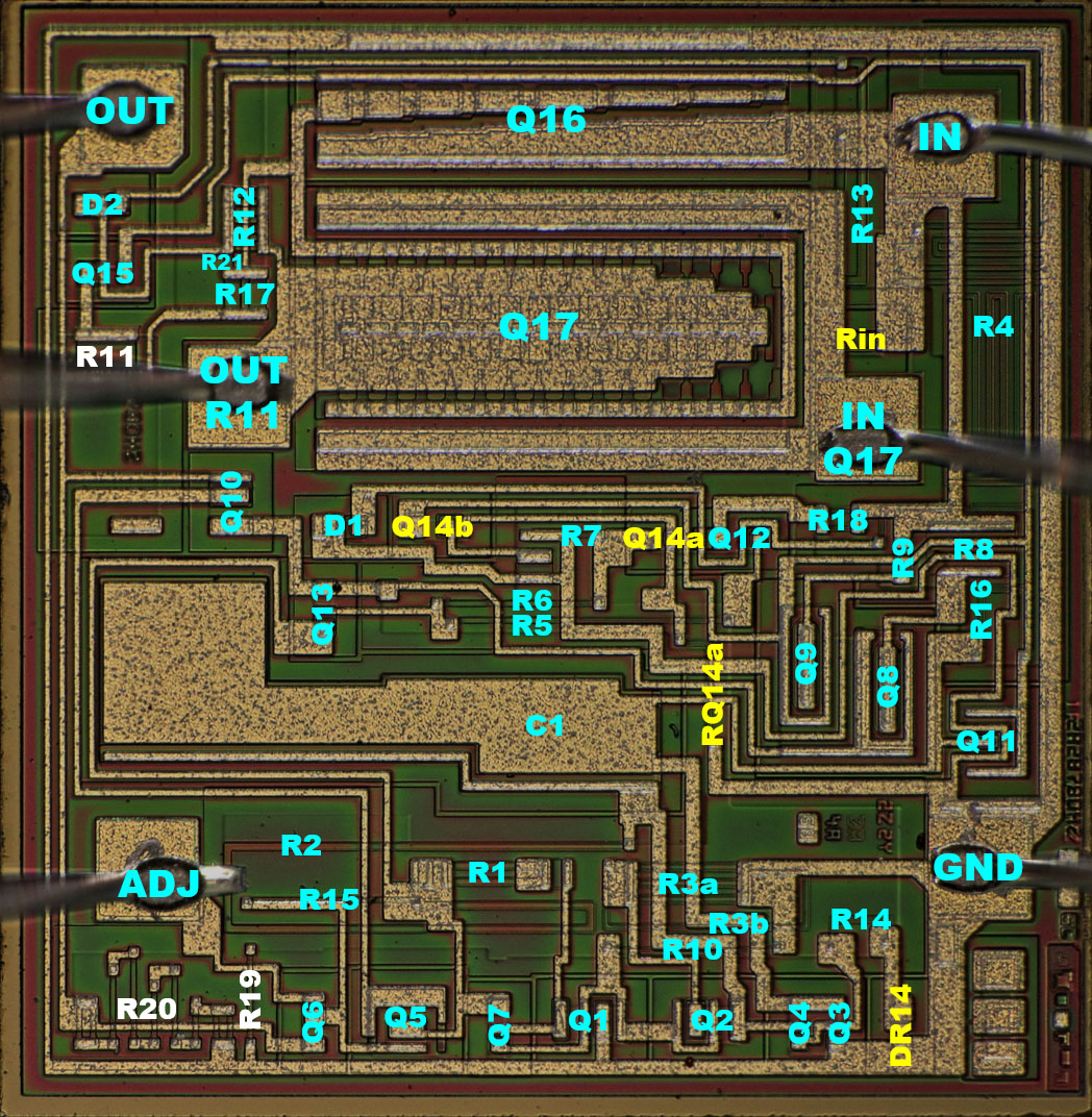
Most of the circuit can be found on the die. The transistor Q14, which represents the overtemperature protection, is designed as a Darlington pair. The DR14 diode can be found in the reference voltage path. This may have reduced the temperature drift even further.


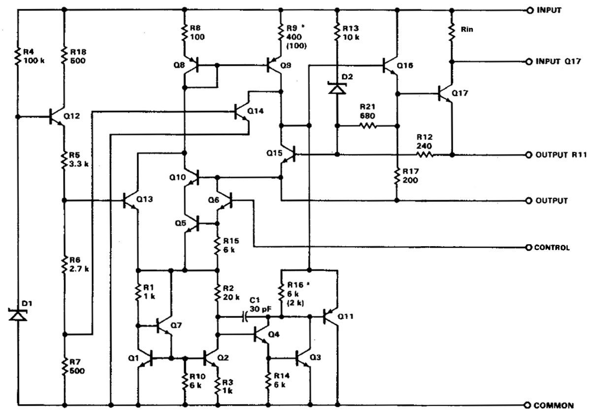
As already described, the µA78M00 has been modified for use with an external transistor. To make the differences clear, the circuit diagram from the Fairchild Voltage Regulator Handbook has been adapted accordingly. The control potential is brought out so that the output voltage can be set externally. The shunt R11 is missing, instead the potential Output R11 is led out, with which an external current limitation can be set up. In addition, the collector of transistor Q17 can be contacted exclusively. This transistor itself represents the series regulator in the original circuit. Isolated from the input voltage, however, it can also be used as a driver for a PNP transistor.


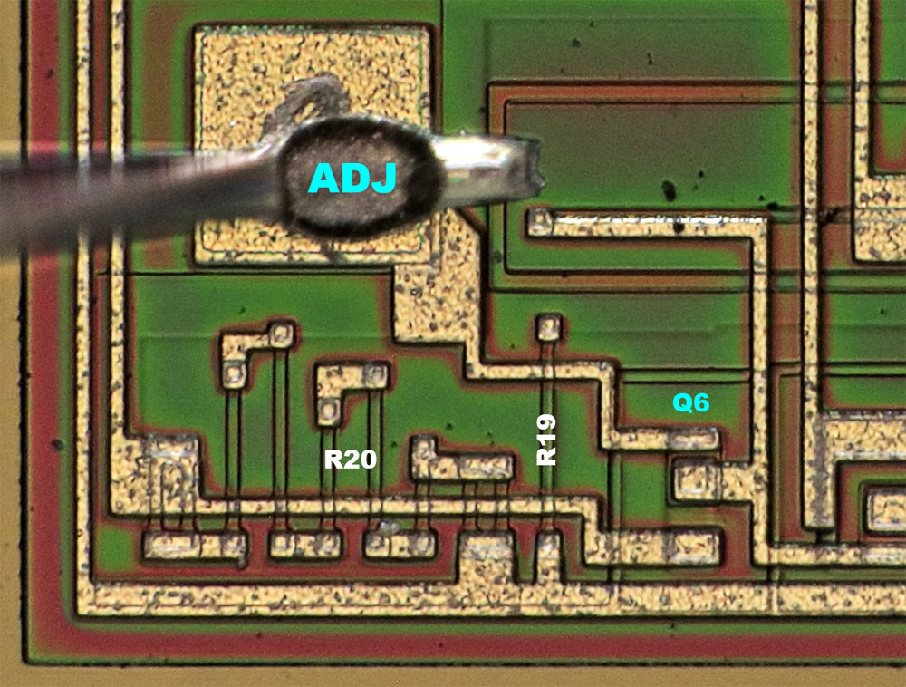
There are two resistors at the lower edge of the die, which can represent the voltage divider for the feedback as R19 and R20 in the fixed-voltage variants. R20 consists of several small elements so that the different output voltages can be set.


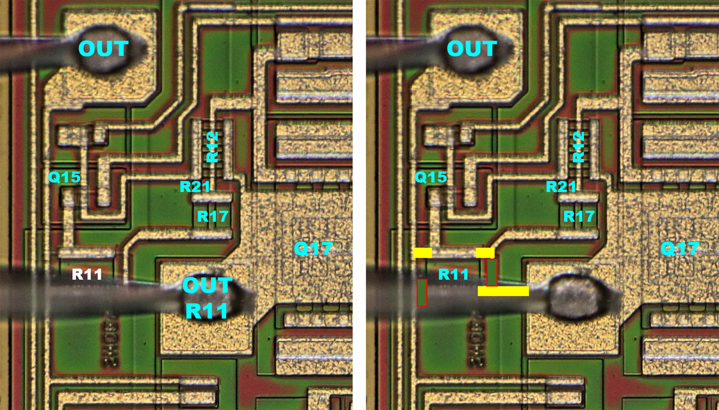
Changing the metal layer is sufficient to integrate the voltage divider for the output voltage into the circuit. The same applies to the integrated series regulator and the shunt R11. In the µA78HG (left), R11 is wired as the emitter resistor of Q15. Its influence in the circuit should not be too great. For applications without an external control transistor, R11 can be integrated as a shunt by making small changes to the metal layer (right). The bondpad OUT R11 is then no longer used. The line to the upper bondpad appears very thin for the output current of 500mA. It may need to be widened to the left. The adjacent GND line is redundant.


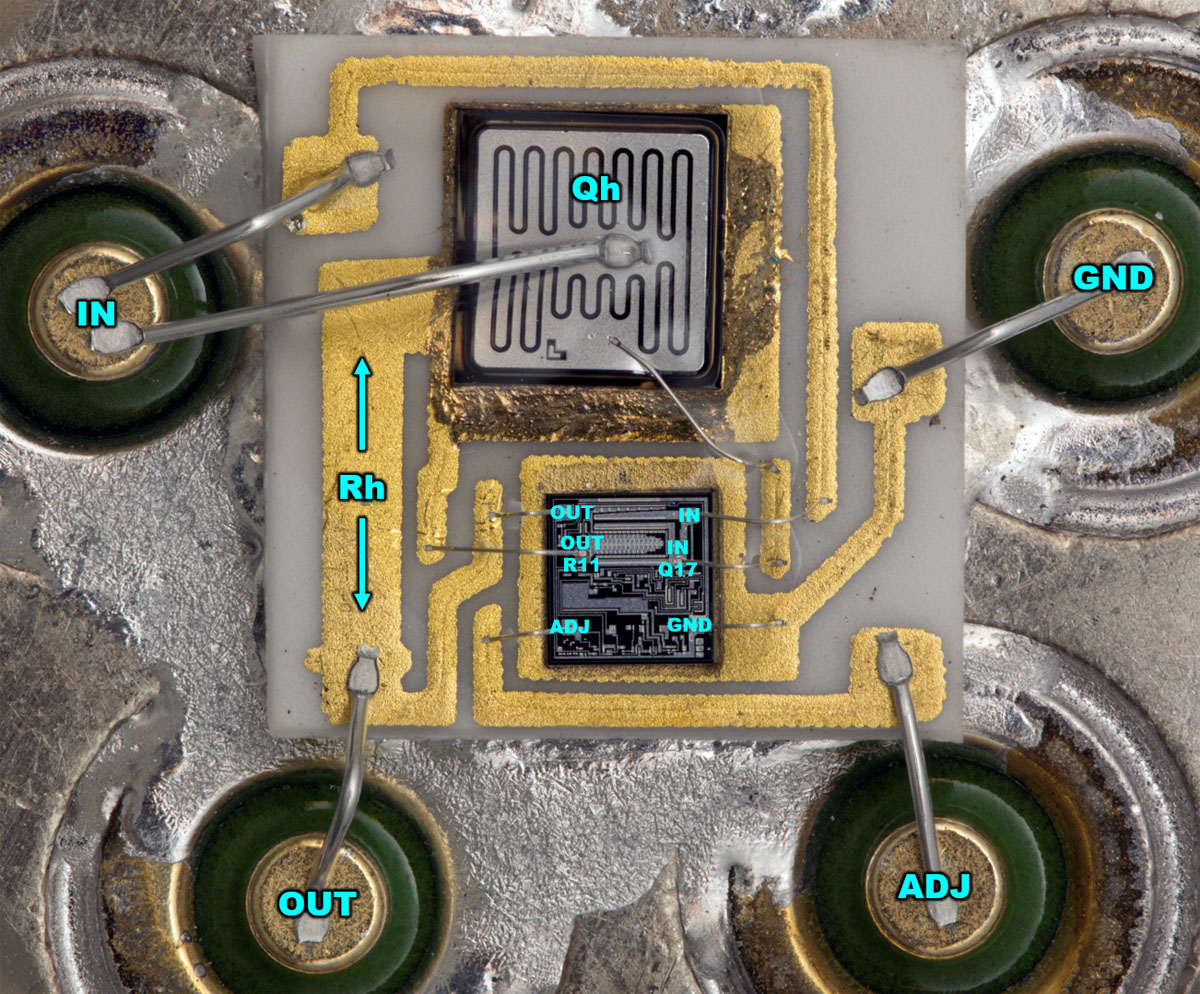
There is a line on the ceramic carrier that serves as the shunt resistor Rh for overcurrent protection.


Somewhat later, another variant of the voltage regulator was introduced with the designation µA78HGA. This does not appear to be just a bin. The A variant is explicitly advertised as pin-compatible.


The µA78HGA datasheet shows a photo of the internal structure. The quality of the photo is very poor, but it appears to show a different structure compared to the regulator shown here. However, it does not necessarily have to be the A variant. It is also conceivable that the picture is just an example and that the first revision with the external current limiter is shown.


https://www.richis-lab.de/voltageregulator24.htm

 :-/O
 
The following users thanked this post: SeanB, Vgkid, doktor pyta, exe, RoGeorge, iMo, D Straney

Online NoopyTopic starter

  • Super Contributor
  • ***
  • Posts: 1735
  • Country: de
    • Richis-Lab
Re: Voltage regulators - die pictures
« Reply #147 on: February 18, 2024, 12:27:27 pm »
I have updated the last picture, the datasheet of the A variant (due to hotlinking the upper post is updated).

There you can see they changed the shunt to a thick film resistor. Perhaps that was the change of the A variant.

Someone gave me the hint that in the second line of the marking there is an A and perhaps that is already the A variant. Well it´s possible but the ending "HGAKC" wouldn´t fit to the datasheet. A year before there was no A variant. The first announcement of the A variant I found was 1982.
Well, I´m not sure and will have to take a closer look...

Offline MarkT

  • Frequent Contributor
  • **
  • Posts: 367
  • Country: gb
Re: Voltage regulators - die pictures
« Reply #148 on: February 18, 2024, 02:05:36 pm »
I am amused that 2.3V is touted as "low drop-out voltage".  According to semiconductor manufacturer's every voltage regulator is "low drop-out", like motor manufacturers' claim that every motor is "high torque".
 

Online NoopyTopic starter

  • Super Contributor
  • ***
  • Posts: 1735
  • Country: de
    • Richis-Lab
Re: Voltage regulators - die pictures
« Reply #149 on: February 18, 2024, 02:13:55 pm »
2,3V is quite a voltage drop but back in the days that probably was not that bad.  :D
 
The following users thanked this post: SeanB


Share me

Digg  Facebook  SlashDot  Delicious  Technorati  Twitter  Google  Yahoo
Smf