Author Topic: Voltage regulators - die pictures  (Read 30429 times)

0 Members and 1 Guest are viewing this topic.

Offline SeanB

  • Super Contributor
  • ***
  • Posts: 16284
  • Country: za
Re: Voltage regulators - die pictures
« Reply #150 on: February 18, 2024, 05:54:15 pm »
Still might have some of those around as well. They were an interesting device for sure. And yes 2V3 was a low dropout voltage, especially when almost all the competition had an absolute minimum dropout of 3V0, and with that the caveat that PSRR would be worse at that voltage, that extra 700mV was a bonus, and also that PSRR was not affected. Meant you could supply a S100 bus card with a single TO3 package regulator on the card, and a smallish clip over heatsink, and still be able to have over 4A of current draw on the card. The alternative was to have a long aluminium strip on the side, and 4 TO220 voltage regulators taking up a good chunk of valuable real estate on the card.
« Last Edit: February 18, 2024, 05:57:57 pm by SeanB »
 
The following users thanked this post: RoGeorge, Noopy

Offline ArdWar

  • Frequent Contributor
  • **
  • Posts: 373
  • Country: sc
Re: Voltage regulators - die pictures
« Reply #151 on: February 18, 2024, 06:00:55 pm »
I am amused that 2.3V is touted as "low drop-out voltage".
This is still rather high even with the original definition of "less than a Darlington drop" hmmm.
 

Offline Gyro

  • Super Contributor
  • ***
  • Posts: 9507
  • Country: gb
Re: Voltage regulators - die pictures
« Reply #152 on: February 18, 2024, 06:25:19 pm »
Remember it was the 1970s and it was a 5A regulator - high for a linear regulator these days.
Best Regards, Chris
 
The following users thanked this post: SeanB

Offline SeanB

  • Super Contributor
  • ***
  • Posts: 16284
  • Country: za
Re: Voltage regulators - die pictures
« Reply #153 on: February 18, 2024, 07:07:04 pm »
Yes, and also the beryllia there is not pink, but white.
 

Offline Gyro

  • Super Contributor
  • ***
  • Posts: 9507
  • Country: gb
Re: Voltage regulators - die pictures
« Reply #154 on: February 18, 2024, 07:46:51 pm »
Yes, a good example for those who automatically interpret pink as Beryllium. I've seen plenty of Beryllium containing ceramic HF power transistors that were white. Low thermal resistance requirement is much more of a guide than color.
Best Regards, Chris
 

Offline quince

  • Newbie
  • Posts: 8
  • Country: de
Re: Voltage regulators - die pictures
« Reply #155 on: February 18, 2024, 08:13:03 pm »
Subscribing :)
 
The following users thanked this post: Noopy

Offline T3sl4co1l

  • Super Contributor
  • ***
  • Posts: 21688
  • Country: us
  • Expert, Analog Electronics, PCB Layout, EMC
    • Seven Transistor Labs
Re: Voltage regulators - die pictures
« Reply #156 on: February 18, 2024, 08:27:25 pm »
Where do people think BeO is pink?  Cr2O3 added to Al2O3 makes it pink.  Al2O3 doesn't need to be pink, it's used pure white often enough, but also often is made pink for vacuum tubes.

I still haven't seen anyone cite standards suggesting/dictating whether this is actually the case, and I haven't seen anything authoritative that suggests BeO was ever colored pink (and the exact shade of pink at that; I don't know if Cr2O3 has the same effect in BeO, or if another element could contribute a similar enough color to be confused with it).

Tim
Seven Transistor Labs, LLC
Electronic design, from concept to prototype.
Bringing a project to life?  Send me a message!
 

Offline NoopyTopic starter

  • Super Contributor
  • ***
  • Posts: 1735
  • Country: de
    • Richis-Lab
Re: Voltage regulators - die pictures
« Reply #157 on: February 18, 2024, 08:53:51 pm »
Where do people think BeO is pink?

Well there were rumors and rumors are often very famous...  ;D

Offline NoopyTopic starter

  • Super Contributor
  • ***
  • Posts: 1735
  • Country: de
    • Richis-Lab
Re: Voltage regulators - die pictures
« Reply #158 on: March 13, 2024, 03:03:30 am »


Now let´s go on with the µA78HG story. The µA78HG shown here was produced in 1980, one year after the µA78HG from 1979. Externally, there are no recognisable differences. But here we definitely have not an "A" version.


It can be seen that the voltage regulator is constructed in exactly the same way as the µA78HG from 1979, although a smaller transistor has been used here as a power transistor.


The edge length of the power transistor is 2,7 mm. It is a MESA transistor, but here not only the outer edges have been etched down, but a trench has been incorporated.


The controller itself does not differ from the µA78HG from 1979.


An artefact catches the eye at the bottom edge. There is dark material on a transistor. It does not appear to be electrical damage. This is contradicted by the loose structure on the surface of the semiconductor and the fact that the metallisation is still intact. It seems more likely that unclean processes have left "dirt" behind or that some kind of corrosion has occurred locally. This would also explain the blackened contact of the resistor placed next to it.


The conspicuous element is transistor Q6. As its base and collector contacts are directly accessible from the outside, it is nevertheless quite conceivable that the transistor has been electrically damaged.


https://www.richis-lab.de/voltageregulator25.htm

 :-/O
 
The following users thanked this post: RoGeorge, ch_scr, Victorman222, quince

Offline RoGeorge

  • Super Contributor
  • ***
  • Posts: 6203
  • Country: ro
Re: Voltage regulators - die pictures
« Reply #159 on: March 13, 2024, 07:43:52 am »
If it were to be a more recent component, everybody will scream 'fake chips' because of the smaller die transistor.  ;D

I was curious about the acronyms for the MESA transistor.  Searched the term because it was also used in the Half-Life game, the underground facility was called "Black Mesa Research Facility".  8)

Turned out the mesa process for transistors is unrelated with Half-Life's Mesa Research Facility, and also not an acronym.  There is an English word 'mesa'.  However, the story is as inciting as the Half-Life opening video:
Quote
In just five months, the founders (1956 Milestone) set up a crystal-growing operation (Sheldon Roberts), developed photolithographic masking techniques using 16 mm movie-camera lenses (Jay Last, Robert Noyce), established the aluminum characteristics needed for making electrical contacts (Moore), and built their own manufacturing and test equipment (Julius Blank, Victor Grinich, Eugene Kleiner) at their Palo Alto facility. Building on their exposure to Bell Labs techniques (1954 Milestone) at Shockley, they developed the first commercial double-diffused (emitter and base) silicon mesa transistor, so named for its raised plateau-like structure. After successful delivery of the Moore team's n-p-n transistor, the device was introduced as type 2N697 to great acclaim at the Wescon trade show in August 1958.
Quote from https://www.computerhistory.org/siliconengine/silicon-mesa-transistors-enter-commercial-production/

With the transistors dies side by side on the screen, they both seems "lifted".  :-//
https://inquivixtech.com/mesa-structure-semiconductor/

Are they both mesa transistors?
« Last Edit: March 13, 2024, 07:46:55 am by RoGeorge »
 
The following users thanked this post: Victorman222, quince

Offline floobydust

  • Super Contributor
  • ***
  • Posts: 7004
  • Country: ca
Re: Voltage regulators - die pictures
« Reply #160 on: March 13, 2024, 05:48:25 pm »
For reference, Fairchild µA78HG78HGA rated 50W 40Vin, 5-24V out 5A, beryllium-oxide substrate. Long live TO-3 4 pinners ;)
 

Offline NoopyTopic starter

  • Super Contributor
  • ***
  • Posts: 1735
  • Country: de
    • Richis-Lab
Re: Voltage regulators - die pictures
« Reply #161 on: March 13, 2024, 06:40:24 pm »
With the transistors dies side by side on the screen, they both seems "lifted".  :-//
https://inquivixtech.com/mesa-structure-semiconductor/

Are they both mesa transistors?

The transistor on the right hand side is a silicon block in which one has diffused a base and a emitter region exactly where they should be. With this way of building a transistor you can get a quite clean base collector junction. Everybody is happy.

Before they were able to build such nice and clean completely diffused transistors they built transistors by doping a "collector doped" silicon block on one side with "base dopant". They did that over the whole area. Now you have a base collector junction that reaches to the rough and dirty outer edges of the transistor. That gives you a lot of leackage current. To avoid this you can etch away the edges or you can etch a trench. That gives you a lot cleaner surfaces. Transistor with such edged structures were called MESA transistors.


For reference, Fairchild µA78HG78HGA rated 50W 40Vin, 5-24V out 5A, beryllium-oxide substrate. Long live TO-3 4 pinners ;)
With an input voltage of up to 40V, the output voltage of the µA78HG can be set between 5V and 24V via a voltage divider. The output current is specified with a maximum of 5A. The short-circuit protection typically kicks in at 7A. Up to 50W can be dissipated.
:-+ ;)
 
The following users thanked this post: RoGeorge, quince

Offline NoopyTopic starter

  • Super Contributor
  • ***
  • Posts: 1735
  • Country: de
    • Richis-Lab
Re: Voltage regulators - die pictures
« Reply #162 on: March 16, 2024, 04:48:44 am »


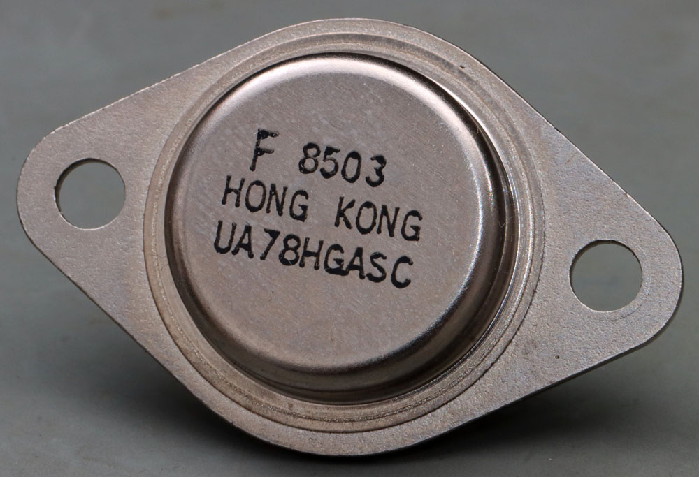
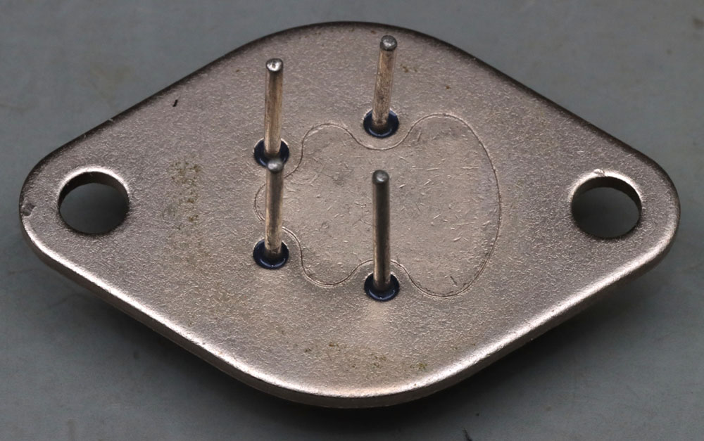
Here you can see the A variant of the µA78HG voltage regulator. In comparison with the µA78HG from 1979 and the µA78HG from 1980, a modern TO-3 housing was already used here. A pressed-in heatspreader can be seen on the underside. Pressed-in heatspreaders are rarely found on modern TO-3 cases. The curved shape is very unusual. This is probably the only way to achieve the necessary thermal conductivity.


The heat spreader is necessary because the base plate of modern TO-3 enclosures is significantly thinner and therefore does not distribute the heat sufficiently over the cooling surface.


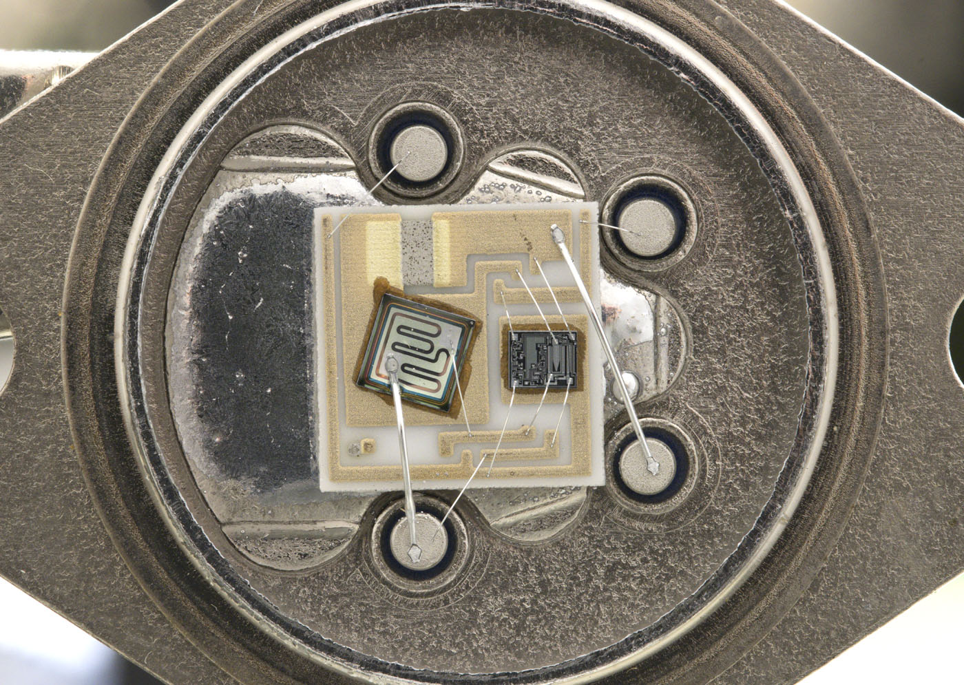
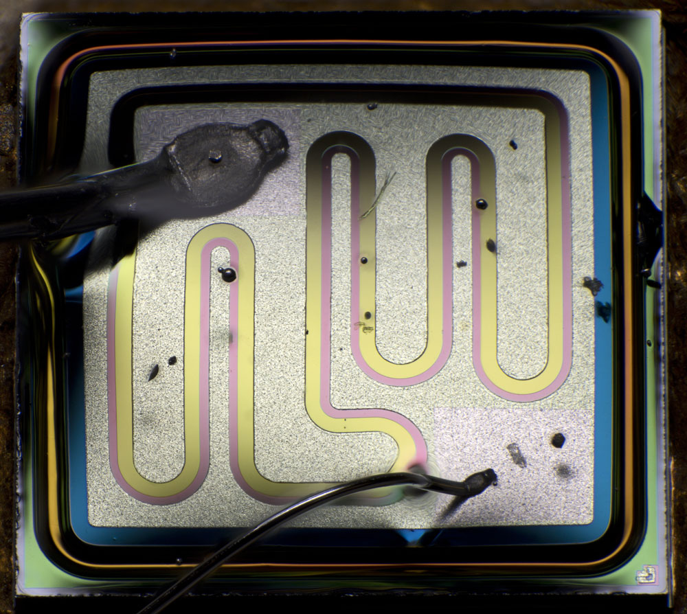
Like the other µA78HG, the µA78HGA also contains a ceramic carrier. In the µA78HGA, thicker bondwires were only used where they were necessary. Thinner bondwires were used where lower currents flow.


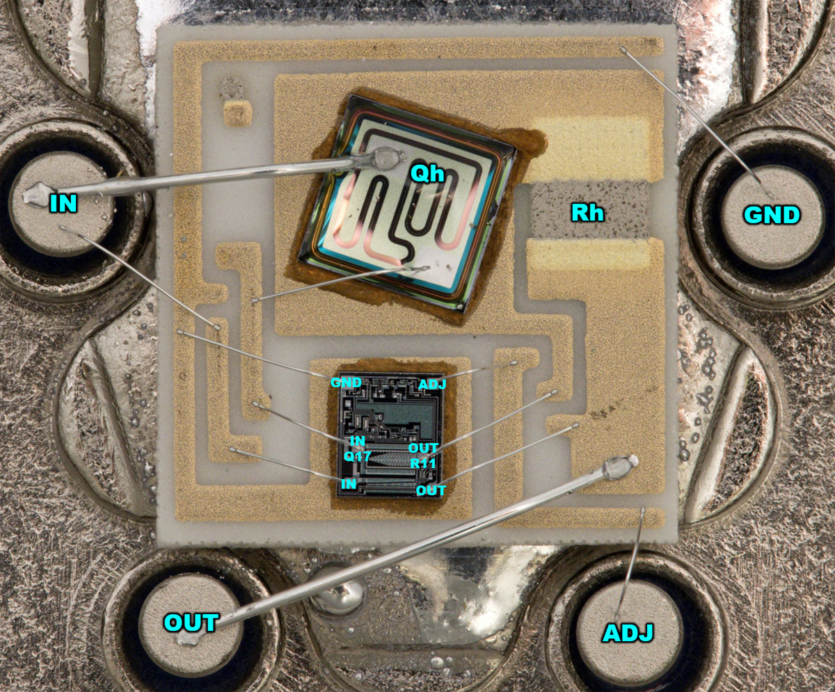
The power transistor is visually similar to the power transistor in the µA78HG from 1980. One major difference in the A variant is the shunt resistor Rh, which is used to limit the current. In the µA78HG, a conductor track of the ceramic carrier was used for this purpose. Here a grey resistor material was used.


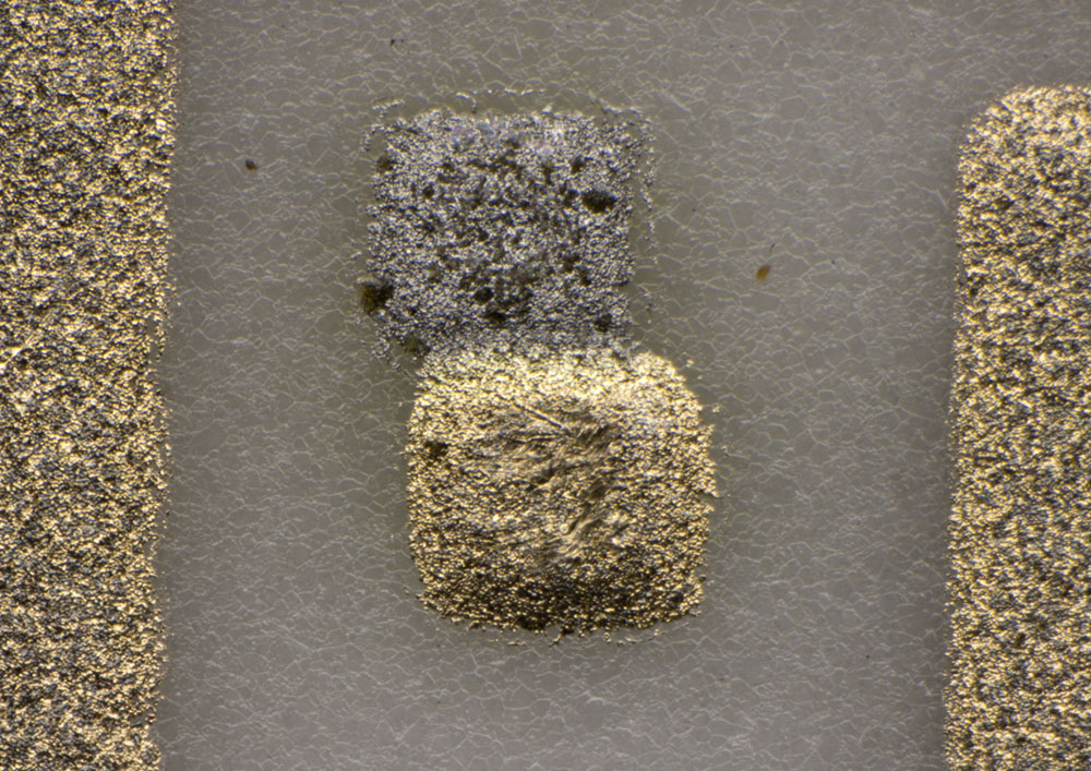
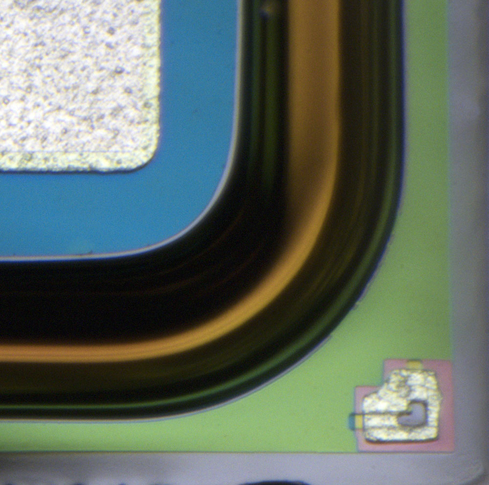
The use of the resistor material has probably made it easier to achieve the desired resistance value. However, the ceramic carrier must be coated with two materials to achieve this. Two squares in the top left-hand corner show how well the resistor material and the metal layer are aligned with each other.


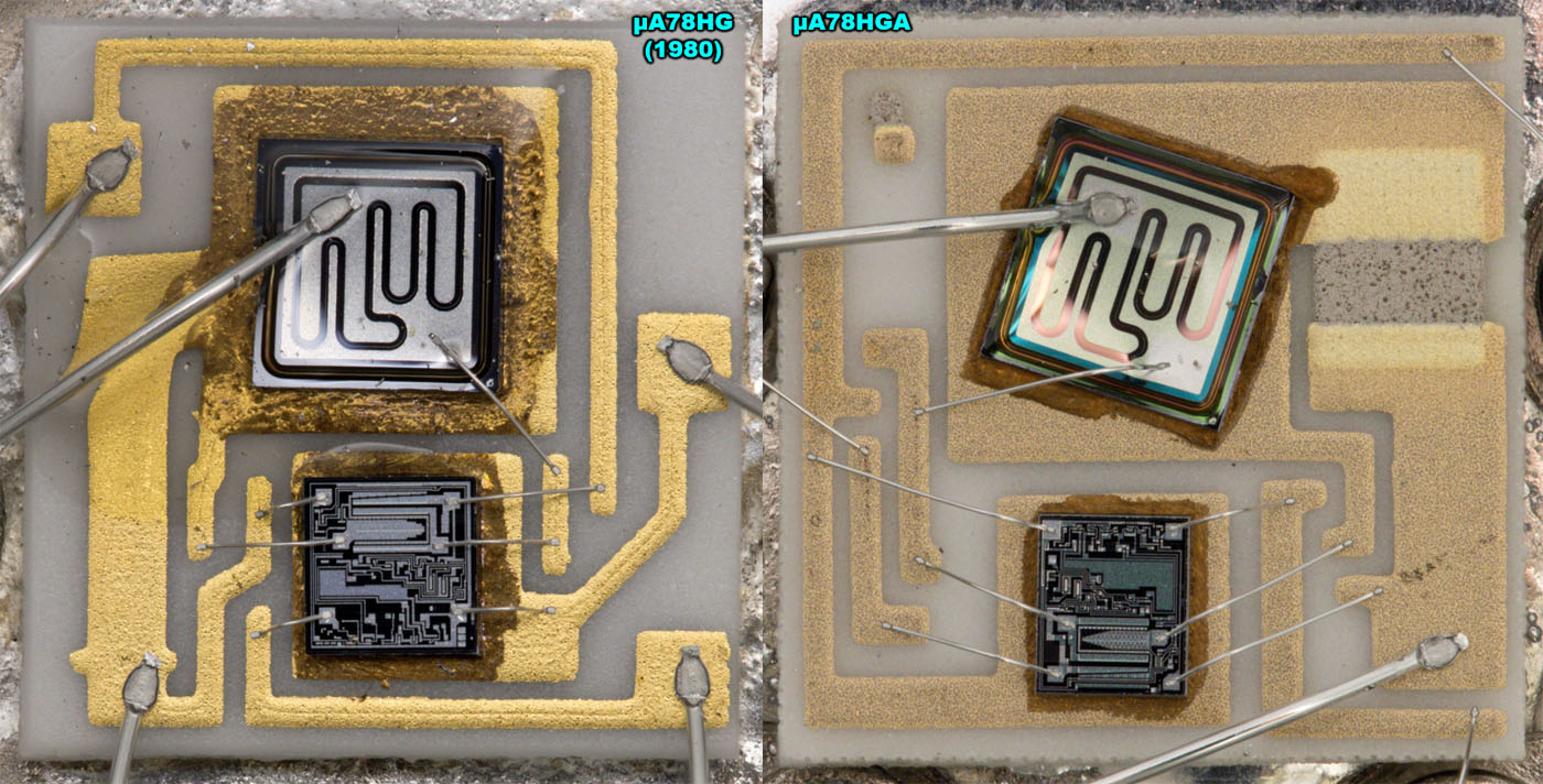
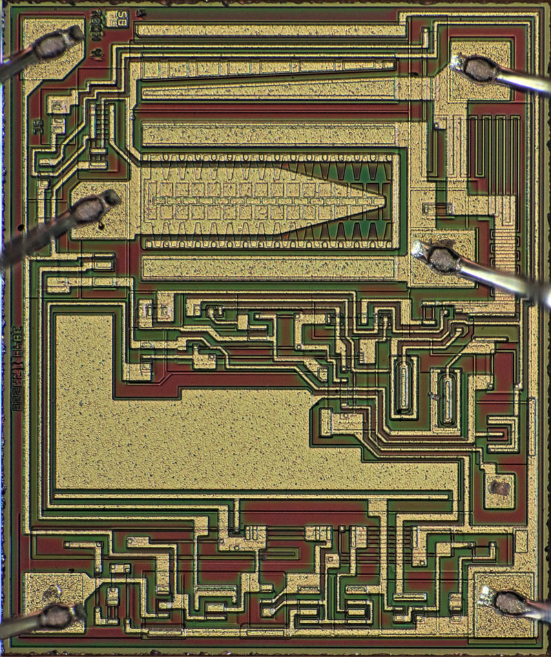
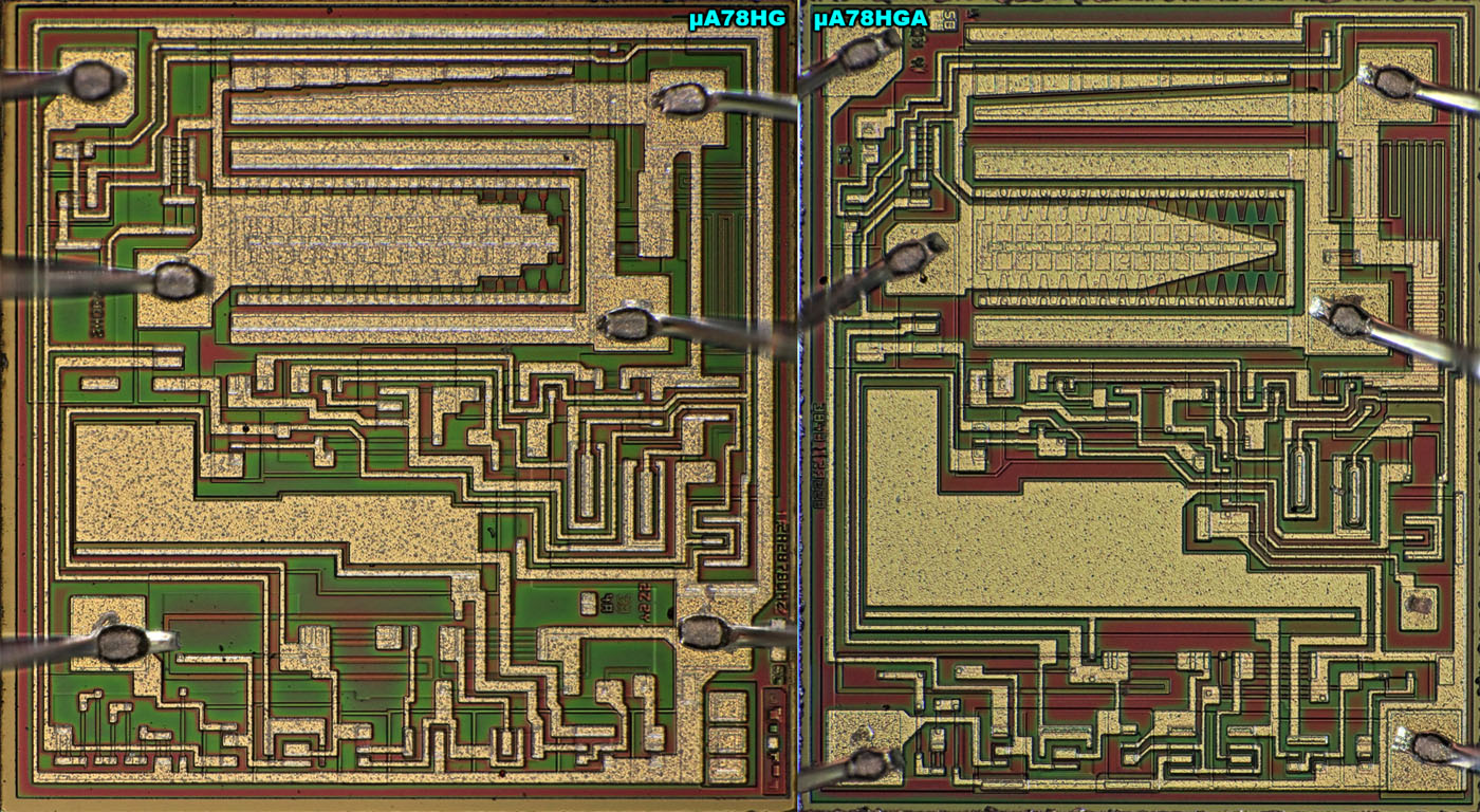
A direct comparison of the µA78HG from 1980 with the µA78HGA shows that the layout has been completely revised. In this context, the controller die has also been rotated by 180°.


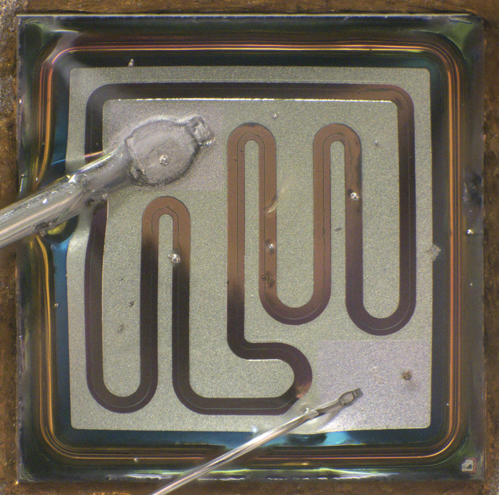
The power transistor is the same type as in the µA78HG from 1980.


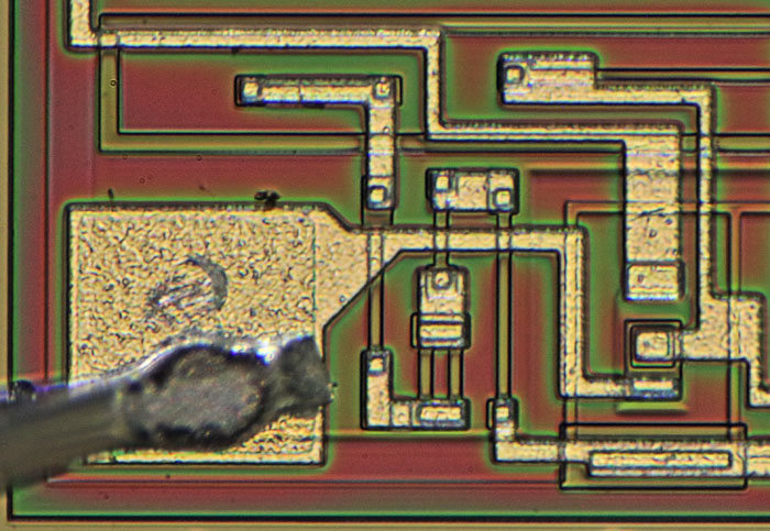
There is an interesting test structure in the bottom right-hand corner of the transistor that can be used to check the alignment of the masks.


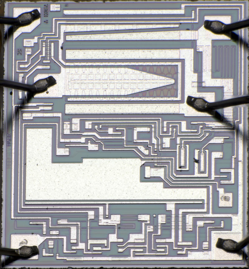
The dimensions of the integrated regulator are 1,6mm x 1,9mm. It is therefore noticeably smaller than the controller type used in the µA78HG from 1979 and the µA78HG from 1980 (1,8mm x 1,9mm).


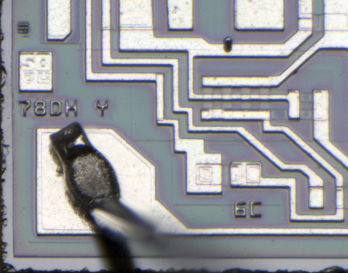
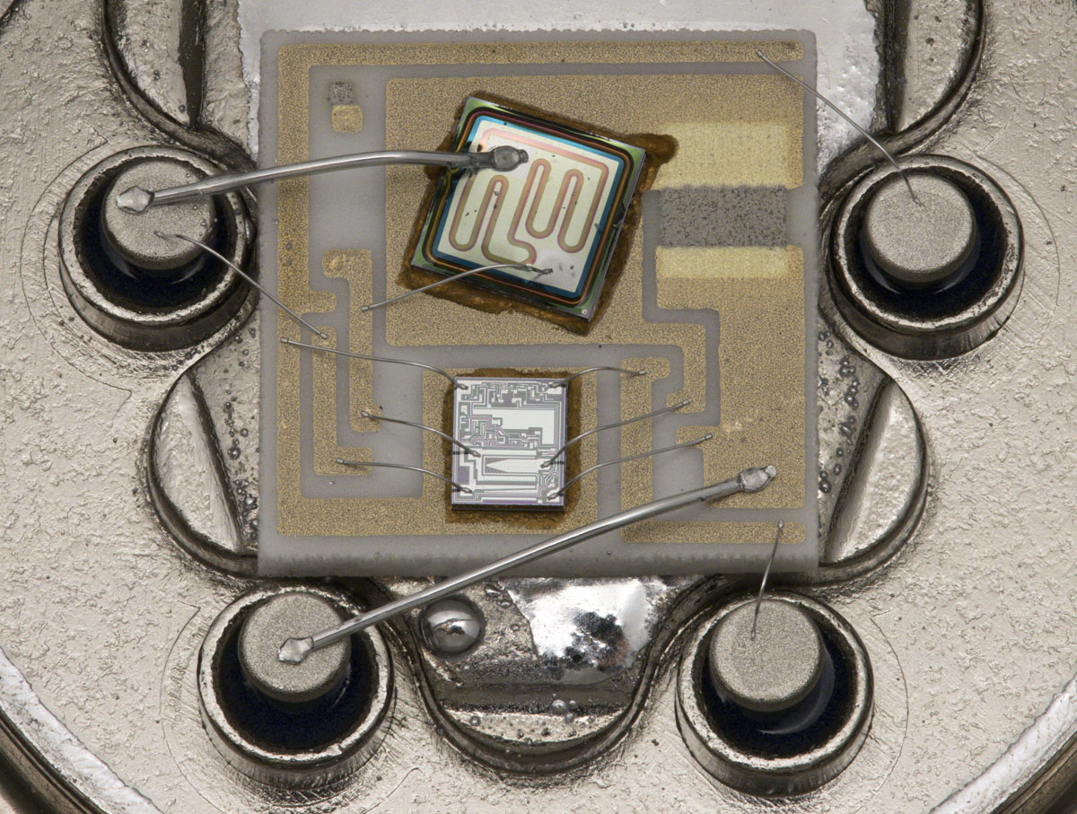
The die shows the letters 78DH Y. The controllers of the older µA78HG were labelled 78DHZ. Apparently the revisions were counted backwards from the letter Z in the direction of A.


If you place revisions Z and Y directly next to each other, you can see that the circuits are essentially the same.


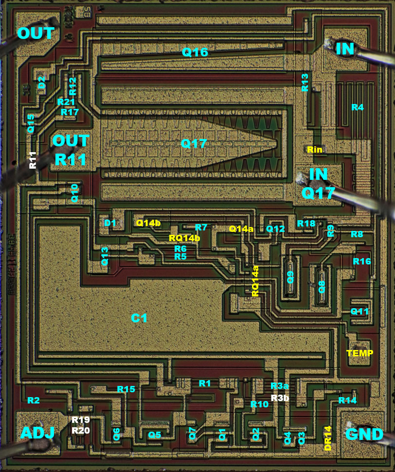
A closer look reveals some minor differences. In the lower right-hand area, the TEMP testpad now offers the option of measuring the potential at the base of transistor Q14. This can be used to determine when the overtemperature protection kicks in. This is helpful as this function is heavily dependent on the tolerance of the resistors.

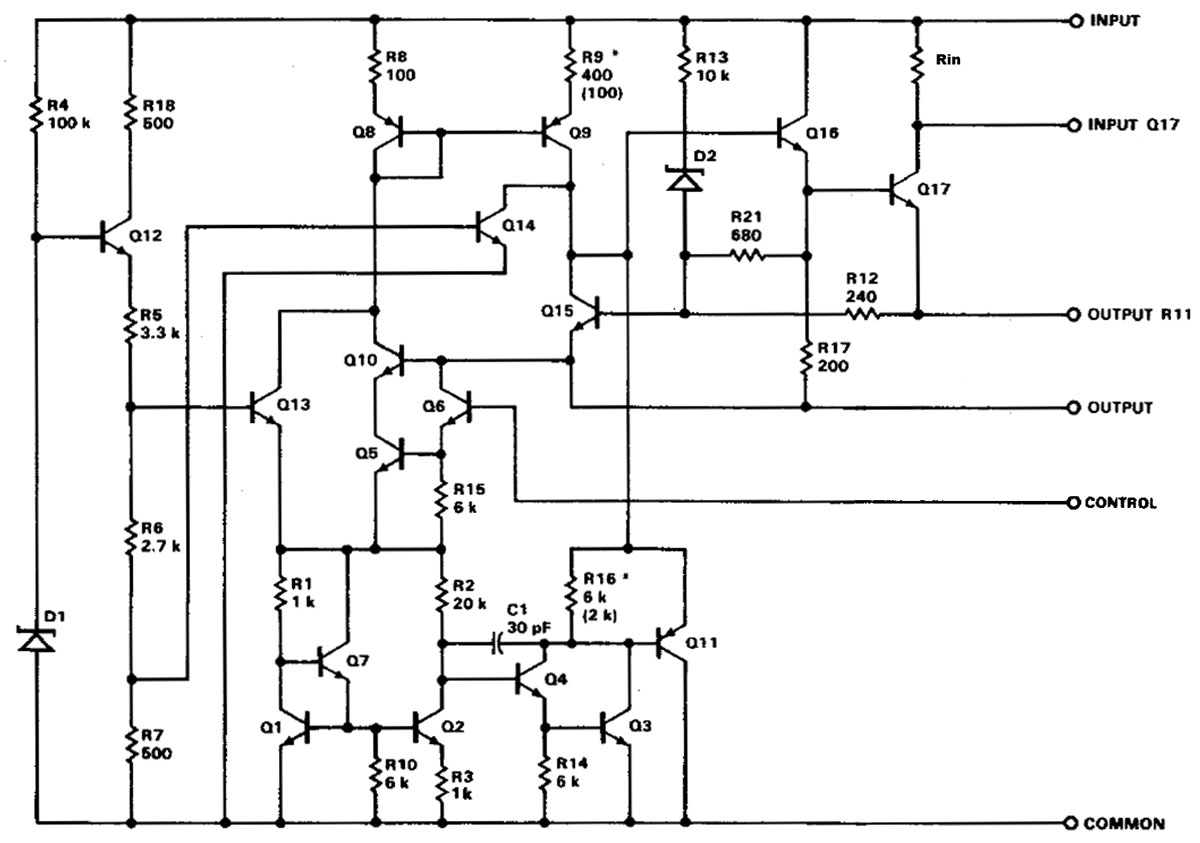
An emitter resistor has been added to transistor Q14b in the circuit. The capacitance C1 has been made larger. The resistor R3, which consists of two elements, defines the proportion of the negative temperature coefficient in the reference voltage generation. In contrast to the older revision, the resistor R3b is not included in the circuit here.


There are some unused resistors in the bottom left-hand corner, which scale the feedback of the output voltage appropriately for fixed-voltage regulators. There are significantly fewer resistors here than in the previous revision. The ends of some resistors are widened so that their values can also be changed by moving the contact.


https://www.richis-lab.de/voltageregulator26.htm

 :-/O
 
The following users thanked this post: RoGeorge, ch_scr

Offline RoGeorge

  • Super Contributor
  • ***
  • Posts: 6203
  • Country: ro
Re: Voltage regulators - die pictures
« Reply #163 on: March 16, 2024, 07:51:39 am »
Very interesting to have for comparison 2 versions of the same chip.

I'm intrigued by the Q17 emitter (thanks for the annotations  :-+).  Is Q17 a set of 15 (or maybe 2x15?) small transistors, all in parallel?  And why such shape, with constant size elements, but smaller and smaller emitter?

Q16 seems about the same, with thinner and thinner emitter, except this time the horizontal spacing also goes larger and larger (from left to right).  What is the idea/the goal for such shapes?

Quote


« Last Edit: March 16, 2024, 07:56:59 am by RoGeorge »
 

Offline NoopyTopic starter

  • Super Contributor
  • ***
  • Posts: 1735
  • Country: de
    • Richis-Lab
Re: Voltage regulators - die pictures
« Reply #164 on: March 16, 2024, 08:28:07 am »
Give me a few hour, I will add an picture explaining what is happening here. In fact the structures are very interesting.  :-+

Offline David Hess

  • Super Contributor
  • ***
  • Posts: 16620
  • Country: us
  • DavidH
Re: Voltage regulators - die pictures
« Reply #165 on: March 16, 2024, 12:43:46 pm »
I'm intrigued by the Q17 emitter (thanks for the annotations  :-+).  Is Q17 a set of 15 (or maybe 2x15?) small transistors, all in parallel?  And why such shape, with constant size elements, but smaller and smaller emitter?

Q16 seems about the same, with thinner and thinner emitter, except this time the horizontal spacing also goes larger and larger (from left to right).  What is the idea/the goal for such shapes?

Current is proportional to emitter area so I assume this was done to distribute the heating evenly and prevent hot spots.
 

Offline NoopyTopic starter

  • Super Contributor
  • ***
  • Posts: 1735
  • Country: de
    • Richis-Lab
Re: Voltage regulators - die pictures
« Reply #166 on: March 16, 2024, 07:07:40 pm »


The power transistor is constructed in the same way as in many other voltage regulators. The collector potential is supplied at the top and bottom. Below the entire transistor surface there is a buried collector. It can be recognized by the somewhat blurred edge that frames the transistor. The base potential contacts the p-doped base area on two sides, which is located above the n-doped collector.

The emitter, which has a special geometry, is generated in the base area with an n-doping. The emitter area tapers towards the base contacts. A large part of the interaction between base and emitter takes place in this area. As the transistor operates in linear mode, it is important that the current is distributed evenly over the emitter areas. This is ensured by the thin strips of the n-doping. They represent emitter resistors (Re). The metal layer is only contacted in the middle (yellow areas). The collector line for the emitter currents widens from right to left as the current increases.

The driver transistor Q16 is less critical. The geometries of the metal layer are just proportional to the current.
 
The following users thanked this post: RoGeorge

Offline NoopyTopic starter

  • Super Contributor
  • ***
  • Posts: 1735
  • Country: de
    • Richis-Lab
Re: Voltage regulators - die pictures
« Reply #167 on: March 25, 2024, 04:18:48 am »


With the µA78MG, Fairchild had a variable voltage regulator in its programme that allows a continuous output current of 0,5A. The datasheet specifies a peak current of 0,8A. Here you can see the housing variant known as the Power Mini Dip. It features two wide metal strips that dissipate the heat from the regulator. The strips are connected to the input potential. In addition to the Power Mini Dip, the µA78MG was also available in a TO-39 and a Power Tab housing (TO-220).


The dimensions of the die are 1,7mm x 1,9mm.


The character sequence 78MGZ is shown in the bottom left-hand corner. The Z probably stands for a first revision of the design. Next to the bondpad is a B, the meaning of which is not clear.


Here you can see a comparison of the µA78MG (right) with the controller in the µA78HGA (left). Apart from the adaptation to an external power transistor, the controller of the µA78HGA works with the same circuit as the µA78MG. The structures are also very similar, although the testpoint for overtemperature protection is missing.

The Fairchild Voltage Regulator Handbook from 1978 explains that the µA78HG are constructed with the µA78MG00 regulator and an external power transistor. As described with the 1979 µA78HG (https://www.richis-lab.de/voltageregulator24.htm), it is possible that this was initially the case.


https://www.richis-lab.de/voltageregulator27.htm

 :-/O
 
The following users thanked this post: RoGeorge

Offline NoopyTopic starter

  • Super Contributor
  • ***
  • Posts: 1735
  • Country: de
    • Richis-Lab
Re: Voltage regulators - die pictures
« Reply #168 on: April 24, 2024, 03:47:40 am »


The µA79MG corresponds functionally to the µA78MG, but regulates a negative voltage. The output voltage can be set between -2.2 and -30V. The Power Mini Dip package was available in three versions: T-1, T-2 and T-3. The µA78MG documented here uses the T-2 variant, which has a angled metal tab on each side. The µA79MG shown here uses the T-3 variant, which only has one straight metal tab. In the T-1 variant, two metal tabs are bent downwards so that they can be soldered to the circuit board.


The dimensions of the die are 1,9mm x 2,0mm.


Several masks are depicted on the right edge. In the lower area there is a character string which is presumably 79MGZ.


The datasheet shows the typical circuit of a 79xx voltage regulator. The operation of the circuit is described with the Mikroelektronika Botevgrad 7915 (https://www.richis-lab.de/voltageregulator20.htm). The µA79MG differs from this only in minor details.


The circuit on the die corresponds to the illustration in the circuit diagram. A series of resistors are integrated in the right-hand area, which can be used to represent a fixed-voltage regulator. To the left of these resistors is an unused capacitor, which probably stabilises the feedback loop.

The capacitor C2 appears to be divided into two areas. The n-doped buried collector is used, which represents the desired capacitance with the p-doped substrate.


A transistor and a few resistors are integrated in the bottom left corner of the µA79MG, which have no effect on the circuit. The Fairchild Voltage Regulator Handbook from 1978 contains the circuit diagram of the µA79M00 fixed-voltage version. There, the additional components are used to represent a different tapping of the reference voltage for the higher output voltages. The higher reference voltage ensures that the feedback voltage divider does not reach too extreme resistances at high output voltages, which worsens the control behaviour. In order to be able to display the full output voltage range with the µA79MG, the low reference voltage must be selected.


There are two discolourations in the power transistor which indicate that the voltage regulator was defective.


https://www.richis-lab.de/voltageregulator28.htm

 :-/O
 
The following users thanked this post: RoGeorge, iMo, quince


Share me

Digg  Facebook  SlashDot  Delicious  Technorati  Twitter  Google  Yahoo
Smf