Author Topic: Voltage regulators - die pictures  (Read 87726 times)

0 Members and 7 Guests are viewing this topic.

Offline magic

  • Super Contributor
  • ***
  • Posts: 8064
  • Country: pl
Re: Voltage regulators - die pictures
« Reply #175 on: November 15, 2024, 10:11:54 pm »
Maybe slightly better ;)

But WTF is this circuit here? I gather the first MOSFET pair is a P-ch current mirror (gate shorted to "southern" drain) and the next is an N-ch differential pair, and they drive the output FET directly. Pretty obvious so far.

The rest must be the voltage reference, and what exactly happens here? Looks like the current source from the simplified schematic is a series pair of N-MOS with gates shorted to sources (or floating?), and the "resistor" is a diode connected(?) N-MOS. And this is supposed to produce a constant voltage? :-//
« Last Edit: November 15, 2024, 10:17:31 pm by magic »
 

Offline NoopyTopic starter

  • Super Contributor
  • ***
  • Posts: 2406
  • Country: de
    • Richis-Lab
Re: Voltage regulators - die pictures
« Reply #176 on: November 16, 2024, 04:08:20 am »
The circuit is really extremly simple.
It seems like it is just a very simple differential amplifier looking at something like a zener reference with a resistor "current source".
If you balance everything as good as possible that is perhaps stable enough.

Offline NoopyTopic starter

  • Super Contributor
  • ***
  • Posts: 2406
  • Country: de
    • Richis-Lab
Re: Voltage regulators - die pictures
« Reply #177 on: February 19, 2025, 07:11:51 pm »
I have an update for the B260 (GDR version of the TDA1060).


There are a total of three mask sets: 03, 04 and 05. Mask set 03 was used in July 1984 (R7), January 1985 (T1) and March 1985 (T4). The B260 from May 1986 (U5) is still based on mask set 03, but here the revision counter of the metal layer now shows a 2, whereas previously all revision counters were still at 1.

Mask set 04 appears in December 1987 (VD) and March 1988 (W3). The VD component bears the designation TDA1060. It was quite common for ICs to be produced for the West and printed with the Western designation. This is not a counterfeit. They didn´t mark it with a Philips logo.

The mask set 05 can finally be found in the B260 which was produced in June 1990 (A6).

It is interesting to note that there are no functional differences between the revisions. The two 03 variants appear completely identical. The small squares on the edges of the 04 mask set, which show the alignment of the masks, are missing. The small test structures on the upper edge are also missing. Furthermore, the testpad in the bottom left corner is now smaller and the connection of some bondpads has been slightly modified. The process seems to have changed for variant 05. The structures are unchanged, but the contacts to p-doped surfaces, which form the base for NPN transistors, are visually very different. The contact surfaces are smoother and larger.


The B260 built in March 1985 (T4) was severely damaged at pin 5.


https://www.richis-lab.de/voltageregulator17.htm#v

 :-/O
 
The following users thanked this post: RoGeorge

Offline NoopyTopic starter

  • Super Contributor
  • ***
  • Posts: 2406
  • Country: de
    • Richis-Lab
Re: Voltage regulators - die pictures
« Reply #178 on: February 21, 2025, 04:41:10 pm »


On closer inspection of the marking, it quickly becomes clear that this component is fake. The resolution was not sufficient to reproduce the Philips logo cleanly.


The package contains a B260 from the Halbleiterwerk Frankfurt Oder. The TDA1060 and the B260 are functionally identical. The counterfeit component could probably be used as normal one.


Here is another very interesting counterfeit part. The combination of the designation TDA1060 with the logo of the Halbleiterwerk Frankfurt Oder would still be plausible so far, although the logo looks a little inaccurate. However, the HFO always used an alphanumeric code consisting of two characters as a datecode. What looks like a datecode here is also implausible. According to this, the TDA1060 would have been produced in 1999. At that time, however, the Halbleiterwerk Frankfurt Oder had long since disappeared.


This TDA1060 also contains a B260.


https://www.richis-lab.de/voltageregulator29.htm

 :-/O
 
The following users thanked this post: RoGeorge, D Straney

Offline NoopyTopic starter

  • Super Contributor
  • ***
  • Posts: 2406
  • Country: de
    • Richis-Lab
Re: Voltage regulators - die pictures
« Reply #179 on: June 11, 2025, 07:24:46 pm »


Now we have a genuine Philips TDA1060.


The dimensions of the die are 2,3mm x 1,8mm. Some characters are shown in the bottom left corner. The structures are very similar to those in the HFO B260. However, it is clearly recognizable that the masks were not simply copied. The circuit has been recreated using their own process.


https://www.richis-lab.de/voltageregulator30.htm

 :-/O
 
The following users thanked this post: RoGeorge

Offline NoopyTopic starter

  • Super Contributor
  • ***
  • Posts: 2406
  • Country: de
    • Richis-Lab
Re: Voltage regulators - die pictures
« Reply #180 on: October 13, 2025, 03:21:27 am »


I have added another revision of the B260. The mould compound was a little hard to remove, sorry...  ^-^
M8 stands for August 1980 and it uses even another revision, the revision 02.
Now we have 02, 03_1, 03_2 , 04 and 05 and still no functional difference.


https://www.richis-lab.de/voltageregulator17.htm#v

 :-/O
 
The following users thanked this post: RoGeorge

Offline NoopyTopic starter

  • Super Contributor
  • ***
  • Posts: 2406
  • Country: de
    • Richis-Lab
Re: Voltage regulators - die pictures
« Reply #181 on: October 26, 2025, 12:02:58 pm »


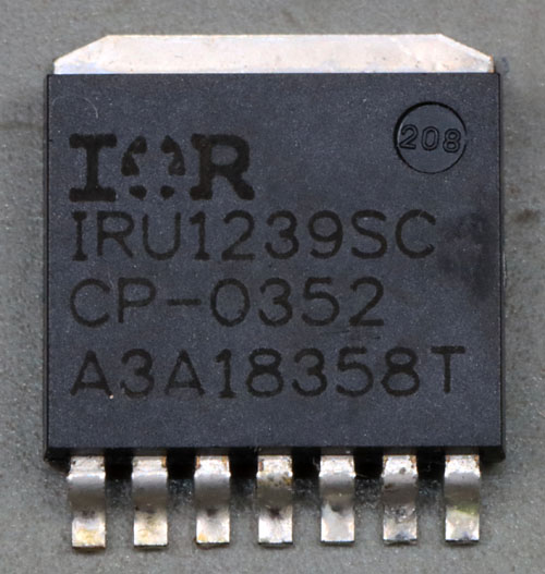
The IRU1239 is a voltage regulator found on Western Digital's WD800BB hard drive.
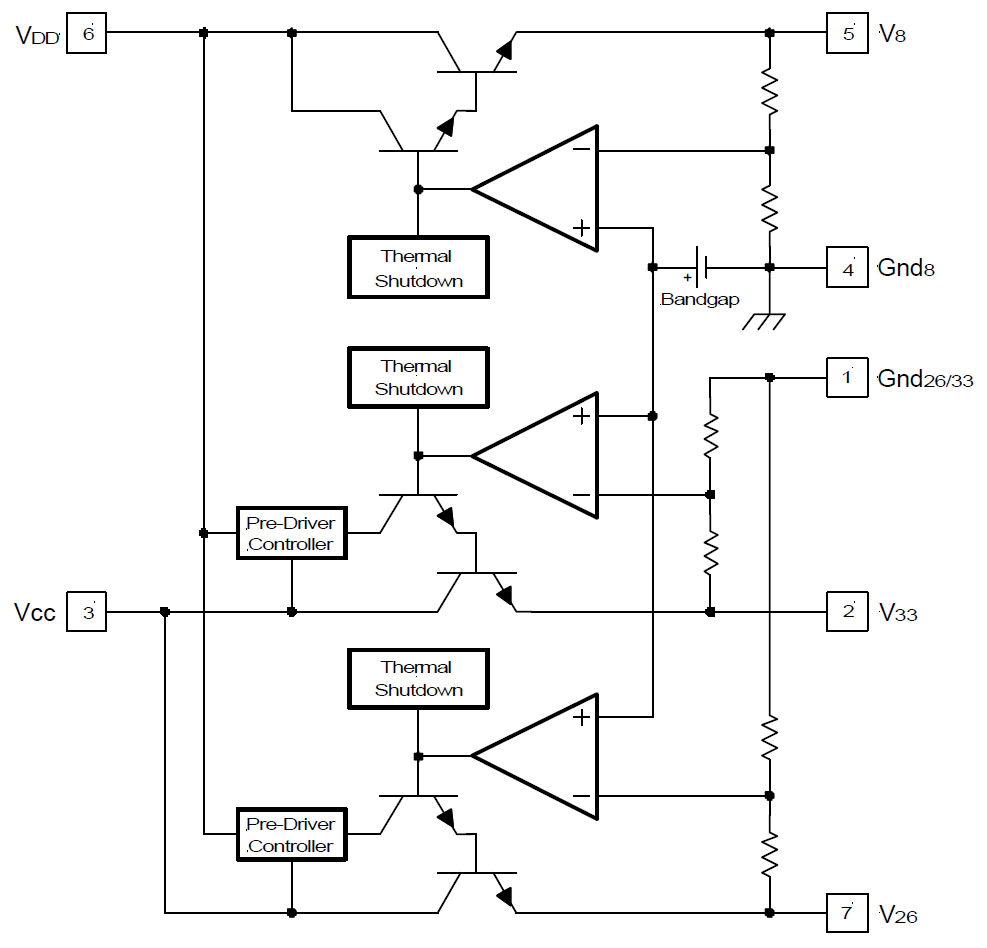


There is no datasheet for the IRU1239. The block diagram above is taken from the datasheet for the IRU1237, which was also developed for use in hard drives and may have a similar design. The IRU1237 contains three voltage regulators with output voltages of 8V, 3,3V, and 2,6V. The current delivery capacity is specified as 0,2A, 1,2A, and 1,2A. The 8V voltage regulator has its own power supply input so that the lower voltage regulators can be supplied with a lower voltage. The lower two voltage regulators also have their own isolated reference potential.

In a Polish forum, the following voltages were measured on the pins of the IRU1239 (pins 1-8) on the WD800BB hard drive: 1.2V / 3.3V / 5.0V IN / 0.0V GND / 1.2V / 12V IN / 2.6V
(https://www.elektroda.pl/rtvforum/topic367631.html#1876064)

Looking at the IRU1237, the potentials raise a few questions. The IRU1239 would therefore generate a 1,2V potential from the 12V supply. The large difference between the input and output voltage is surprising. If the circuit basically corresponds to the IRU1237, then it could be that the circuit on this channel requires a higher voltage. The other two channels could continue to generate 3,3V and 2,6V from the 5V supply. It would then be questionable whether the measurement at pin 1 was incorrect. It is said there was a voltage of 1,2V on the WD800BB PCB. It is conceivable that they modified the output voltages with this potential at the reference point of the lower voltage divider. A higher potential at the reference point of the voltage divider reduces the output voltage. However, this would mean that the lower voltage regulators normally regulate 4,5V and 3,8V. These would be very unusual voltages. In addition, the IRU1237 requires at least 5,25V to be able to deliver its full output current at 3,3V. For voltages above 3,3V, at least this regulator requires more than 5V at the input.
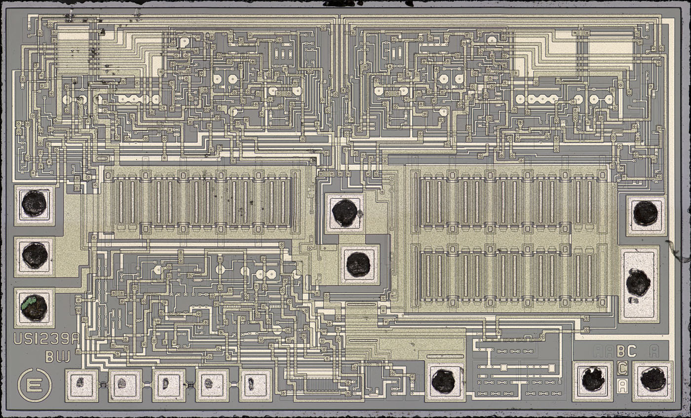


The dimensions of the die contained are 2,2mm x 1,3mm. The designation US1239A is shown in the lower left corner. The letters BW cannot be assigned. In the lower right corner, there are revisions of seven masks. Two metal layers were used.

This image is also available in a higher resolution: https://www.richis-lab.de/images/vreg/35x03XL.jpg (33MB)
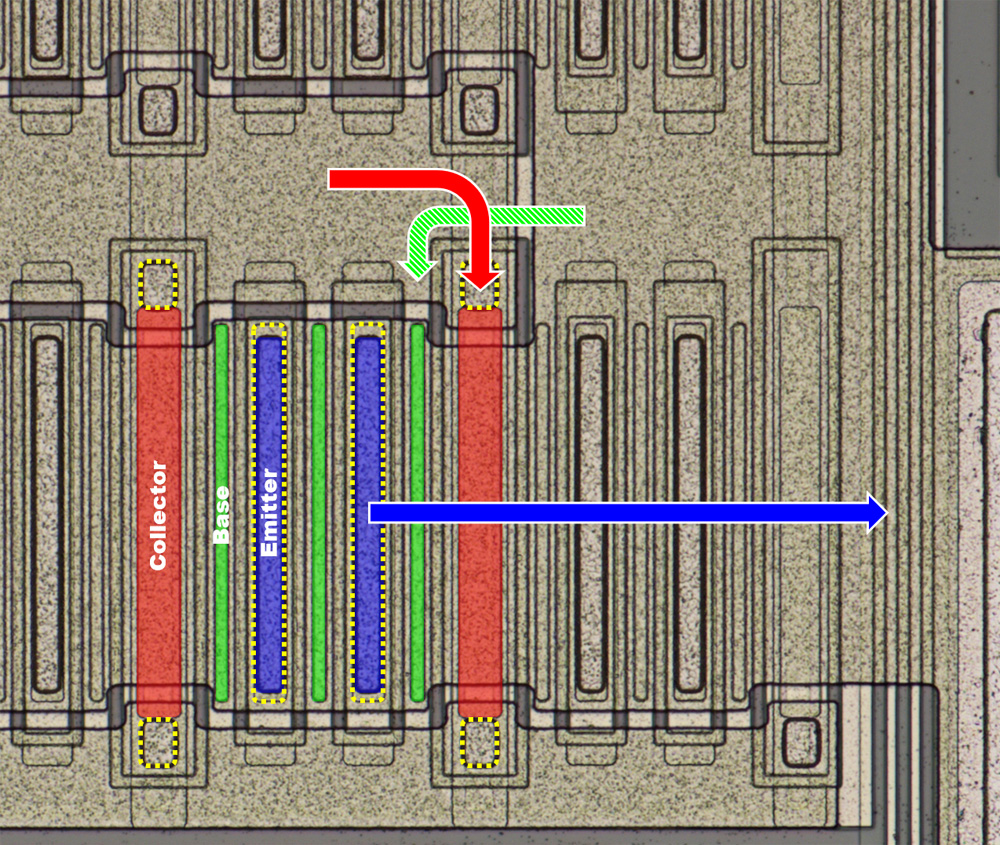


Large power transistors are integrated in the center. The two metal layers enable efficient current conduction. One element of the power transistors consists of two emitters. The elongated contacts are clearly visible (blue). There are strips of the lower metal layer that are connected to the upper metal layer via vias (yellow). From there, the current is conducted to the right via wide lines. The emitter contacts are surrounded by base contacts (green). The base potential of the transistor is connected to the lower metal layer. The base current is supplied within this layer from above and below. The collector current (red) flows in wide strips of the upper metal layer on both sides of the power transistor. Vias provide connections to the lower metal layer, where a strip leads across the collector contact.
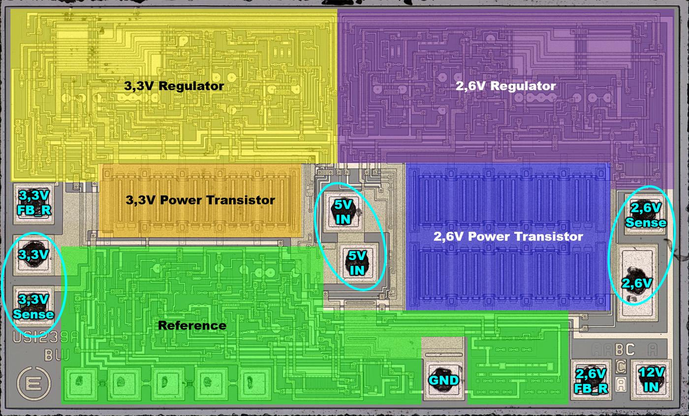


Upon closer inspection and with measurements taken at the pins, the circuit can be reconstructed as follows. The 5V potential enters the circuit in the middle. To the left and right, the current passes through two power transistors. The right transistor is twice as large as the left transistor. These are a 3,3V voltage regulator and a 2,6V voltage regulator. The two regulators are located above their power transistors.

In addition to the actual outputs, each regulator has an input through which it reads back the respective output voltage. The potentials are fed to voltage dividers located in the center of the upper edge. A special feature is the fact that the divided actual voltages are connected with two pins. This also reveals the internal reference voltage with which the regulators operate. This explains the two 1,2V potentials at pins 1 and 5. This is not a third voltage regulator. Presumably, the potentials have been routed to the outside so that the output voltages can be adjusted slightly if necessary.

The reference voltage is generated in the lower section. In the middle of this area you can see the striking transistor combination of a bandgap reference. Fuses on the left offer adjustment options. Both the voltage reference and the regulators use the 12V supply potential.


https://www.richis-lab.de/voltageregulator31.htm

 :-/O
 
The following users thanked this post: RoGeorge, D Straney, Zoli, BILLPOD, AnalogTodd

Offline magic

  • Super Contributor
  • ***
  • Posts: 8064
  • Country: pl
Re: Voltage regulators - die pictures
« Reply #182 on: December 30, 2025, 07:59:24 pm »
LGE (?) LM317L

Low current version of everyone's favorite adjustable linear regulator. I don't know who made this chip, it was a TO92 simply labeled "LGE LM317L". There is a Chinese company called LGE, but they supposedly make discrete power transistors and diodes for the automotive market, so slightly different stuff.

The chip looks like any other 317 and circuitry is similar to the National LM317 shown in the first post here. On the "bottom" we have a standard bandgap reference: two NPNs with 1:8 emitter ratio, bases connected to one of the OUT pads and a chain of resistors goes from the emitters to the ADJ pad in the corner. In the opposite corner there are compensation caps, realized as junction capacitance. The bandgap cell is loaded with a PNP current mirror and drives a sequence of PNP and NPN emitter followers and ultimately the power transistor's base.

Above there is a multi-output PNP current mirror for biasing things, internal reference current generator (with another 8-emitter transistor in it) and thermal throttling. The top is of course the Darlington power transistor and its emitter ballasting resistors. The circuit in the corner is SOA limiting, it looks like a series of two zeners and a resistive divider connected between Vin and power transistor base. With suitably high base voltage (load current) and Vin voltage, the divider turns on a small NPN which steals current from the base.

I thought this SOA protection would be aggressive and quickly limit possible current above 12V, but I actually tested a second identical chip with 20V voltage differential and it was still able to pass 120mA (10Ω between OUT and ADJ), at least for a few seconds before it overheated and started to throttle down. So I guess it protections work fine and aren't getting in the way of normal use. The chip was able to pass 120mA at 8V differential, dissipating about 1W. Probably can't expect more from TO92. Die size is just a bit over 1x1mm.
 
The following users thanked this post: exe, RoGeorge, D Straney, Noopy

Offline David Hess

  • Super Contributor
  • ***
  • Posts: 19220
  • Country: us
  • DavidH
Re: Voltage regulators - die pictures
« Reply #183 on: December 30, 2025, 09:00:13 pm »
I thought this SOA protection would be aggressive and quickly limit possible current above 12V, but I actually tested a second identical chip with 20V voltage differential and it was still able to pass 120mA (10Ω between OUT and ADJ), at least for a few seconds before it overheated and started to throttle down. So I guess it protections work fine and aren't getting in the way of normal use. The chip was able to pass 120mA at 8V differential, dissipating about 1W. Probably can't expect more from TO92. Die size is just a bit over 1x1mm.

Bob Pease mentioned that the regulators are designed to "hard start" into difficult loads.  Otherwise the overload protection can prevent the regulator from starting into a load which it would otherwise be able to power once the output voltage is reached and the voltage across the regulator falls.  At a minimum, this means that the temperature protection has significant hysteresis.
 

Offline magic

  • Super Contributor
  • ***
  • Posts: 8064
  • Country: pl
Re: Voltage regulators - die pictures
« Reply #184 on: December 30, 2025, 10:32:43 pm »
No, it behaved like a constant temperature regulator. Wait for it to heat it up and output current decreases. Reduce input voltage and it gradually climbs back up. Increase a little and current falls a little.

IIRC we looked at National's LM317 schematic and it appeared to do the same thing.
 

Offline David Hess

  • Super Contributor
  • ***
  • Posts: 19220
  • Country: us
  • DavidH
Re: Voltage regulators - die pictures
« Reply #185 on: December 31, 2025, 01:49:23 am »
No, it behaved like a constant temperature regulator. Wait for it to heat it up and output current decreases. Reduce input voltage and it gradually climbs back up. Increase a little and current falls a little.

IIRC we looked at National's LM317 schematic and it appeared to do the same thing.

I found the quote and I guess he was referring to the LM337.  I wonder if they ever changed the LM317; your measurement suggests not.

Some op amps, but mostly voltage regulators and other linear ICs, have an on-chip temperature limiter.  Thermal shutdown circuits can improve reliability.  If a heavy overload is applied for a long time, or there is no heat sink, or the ambient is just too hot, these circuits detect when the chip's temperature exceeds 150°C and then turn off the output.  The thermal-limiter circuit in the LM117 and other' early power ICs just decreased the output current to a safe dc value to hold the die temperature to around 160°C.  In other cases, these thermal limiters oscillate On and Off with a duty cycle that ensures the 160°C chip temperature.  As we at NSC were about to design the LM137, we looked back and decided the latter characteristic was prefer­ able, so we designed about five degrees of thermal hysteresis into the thermal-limit circuit.  That way, the circuit makes a strong attempt to restart its heavy load with a repetition rate of about 100 Hz.

So, we actually designed an oscillation into this ther­mal-limit circuit, but we never bothered to mention it on the data sheet.  H'mmm, we shouldn't be so sloppy.  I apologize.  I'll do better next time.  (This situation has a bearing on one of my pet peeves: bad data sheets.  I get really cross about bad ones, and I really do try hard and work hard to make good ones. Refer to "How to Read a Data Sheet" (Ref 9) because bad data sheets can get the user into trouble.)
« Last Edit: December 31, 2025, 02:04:52 am by David Hess »
 

Offline AnalogTodd

  • Regular Contributor
  • *
  • Posts: 221
  • Country: us
Re: Voltage regulators - die pictures
« Reply #186 on: December 31, 2025, 02:16:55 am »
So, we actually designed an oscillation into this ther­mal-limit circuit, but we never bothered to mention it on the data sheet.  H'mmm, we shouldn't be so sloppy.  I apologize.  I'll do better next time.  (This situation has a bearing on one of my pet peeves: bad data sheets.  I get really cross about bad ones, and I really do try hard and work hard to make good ones. Refer to "How to Read a Data Sheet" (Ref 9) because bad data sheets can get the user into trouble.)
Bob Dobkin was VERY particular about data sheets. He wanted as much relevant information put into the data sheet as possible so that the customer knew what would happen in any potential situation. The way we wrote our data sheets was to meet what Dobkin called the 'Theory of Minimum Phone Calls". Basically, if something you put in there would reduce customer calls, then it was worthwhile. If you left something out and it meant a lot of phone calls, we would go back and edit the data sheet to include the info.

Case in point: the LT3080 family of regulators uses an internally fixed current source through an external resistor to set the output voltage. The equation is pretty simple: Vout = Iset * Rset. Iset is fixed. We thought that was simple enough. Nope, we got phone calls asking what size resistor to use for a particular output voltage. Now the data sheets include a table of typical output voltages and the resistor values needed for them.
Lived in the home of the gurus for many years.
 

Offline magic

  • Super Contributor
  • ***
  • Posts: 8064
  • Country: pl
Re: Voltage regulators - die pictures
« Reply #187 on: December 31, 2025, 06:35:56 pm »
Some people approach Ohm's law with a healthy dose of skepticism.

Some op amps, but mostly voltage regulators and other linear ICs, have an on-chip temperature limiter.  Thermal shutdown circuits can improve reliability.  If a heavy overload is applied for a long time, or there is no heat sink, or the ambient is just too hot, these circuits detect when the chip's temperature exceeds 150°C and then turn off the output.  The thermal-limiter circuit in the LM117 and other' early power ICs just decreased the output current to a safe dc value to hold the die temperature to around 160°C.  In other cases, these thermal limiters oscillate On and Off with a duty cycle that ensures the 160°C chip temperature.  As we at NSC were about to design the LM137, we looked back and decided the latter characteristic was prefer­ able, so we designed about five degrees of thermal hysteresis into the thermal-limit circuit.  That way, the circuit makes a strong attempt to restart its heavy load with a repetition rate of about 100 Hz.

So, we actually designed an oscillation into this ther­mal-limit circuit, but we never bothered to mention it on the data sheet.  H'mmm, we shouldn't be so sloppy.  I apologize.  I'll do better next time.  (This situation has a bearing on one of my pet peeves: bad data sheets.  I get really cross about bad ones, and I really do try hard and work hard to make good ones. Refer to "How to Read a Data Sheet" (Ref 9) because bad data sheets can get the user into trouble.)


That's interesting, because 100Hz oscillation is something I may have easily missed on a DMM and the results I was seeing could be PWM. The circuit is linear, but if it isn't compensated enough, it may oscillate with duty cycle yielding the target temperature on average.

That being said, I have tested my LM317L again with a scope this time and got flat trace at 0.5VDC. Maybe this undocumented subtlety was missed by some clone manufacturers. Maybe stability of this loop depends on workload.
 

Offline David Hess

  • Super Contributor
  • ***
  • Posts: 19220
  • Country: us
  • DavidH
Re: Voltage regulators - die pictures
« Reply #188 on: January 01, 2026, 10:38:41 pm »
That being said, I have tested my LM317L again with a scope this time and got flat trace at 0.5VDC. Maybe this undocumented subtlety was missed by some clone manufacturers. Maybe stability of this loop depends on workload.

I took what Pease said to mean that the LM317 did *not* have oscillation built into the thermal limit, but that the LM337 and later regulators did because of what they learned on the LM317.

Maybe he was literally referring to the LM117 and the LM217 and LM317 were changed, but your measurement suggests all LM317s shutdown linearly.
« Last Edit: January 01, 2026, 10:41:42 pm by David Hess »
 

Offline NoopyTopic starter

  • Super Contributor
  • ***
  • Posts: 2406
  • Country: de
    • Richis-Lab
Re: Voltage regulators - die pictures
« Reply #189 on: October 07, 2026, 03:02:32 am »


The LT1170 from Linear Technology is a versatile switching regulator with an integrated power transistor. With an input voltage between 3V and 60V, the device allows a maximum current of 5A. The LT1170 shares its datasheet with the LT1171, which is specified for up to 2,5A and the LT1172 with a maximum current capacity of 1,25A. The switching frequency is 100kHz.


The datasheet includes a block diagram showing the typical functional blocks of a switching regulator. The section labeled “ANTISAT” here is a unique feature of the LT1170. It ensures that the switching transistor operates at the saturation threshold, allowing it to turn off much more quickly and efficiently. Details on this circuit can be found in the Application Note 19.


The package contains a die measuring 4,0mm x 2,8mm. The right-hand section houses the switching transistor, which is divided into four blocks. The left-hand section contains the remaining circuit components. It can be assumed that the LT1171 omits the right-hand two blocks of the switching transistor. In the LT1172, two half-blocks are likely used.

Current measurement in the power path occurs only in the lower-left corner of the lower-left switching transistor block. In contrast, the additional emitter of the ANTISAT circuit is distributed across all blocks. At the outer edge of each block, two emitter strips are tapped and routed to the left side of the circuit.

This image is also available in higher resolution: https://www.richis-lab.de/images/vreg/36x03XL.jpg (43MB)


The design dates back to 1988.


The metal layer contains the number sequence 1170 and the letter B.


The circuit contains two sections whose characteristics can be adjusted using fuses. The fuses in the upper section adjust the temperature coefficient of the bandgap reference. The right-hand test point is not part of the circuit. It appears to serve solely as a permanent visual marker on the device.


At the bottom edge, in addition to two fuses, an antifuse is used - a pn junction in the reverse direction that, when subjected to a defined current, is overloaded to such an extent that it remains conductive afterward. The conductive connection can be seen as a thin, light-colored line between the contacts of the metal layer.


The upper-right switching transistor is severely damaged.


A closer examination of the damaged area reveals some interesting details. The incident appears to have caused the most damage to the emitter path of a transistor (red). The discoloration of the metal layer indicates where current flowed uncontrollably from the collector to the emitter (yellow). This may have been the point of origin of the failure. The associated base line also shows extensive damage (blue). The current likely switched over to this line after the emitter line was destroyed.

The damage to the contacts to the local emitter resistors (pink) suggests that the surrounding transistors also began conducting uncontrollably due to the high temperatures. Below the bondpad, the contacts to the emitter resistors were apparently more robust. There, the contact is still intact. In contrast, the path above the corresponding emitter shows severe degradation. The current path is also clearly visible there because the aluminum in the metal layer has formed a veritable bridge (green). Another bridge can be found leading to the base contact and further to the right from the base current distribution to the output of the LT1170 (green).

The transistor block connected to the left has also clearly sustained damage. There, too, migration of the metal layer from the collector to the emitter and base potential is evident.


https://www.richis-lab.de/voltageregulator32.htm

 :-/O
« Last Edit: October 08, 2026, 03:21:39 am by Noopy »
 
The following users thanked this post: xrunner, RoGeorge, iMo, D Straney, mawyatt, AnalogTodd

Offline ArdWar

  • Frequent Contributor
  • **
  • Posts: 733
  • Country: sc
Re: Voltage regulators - die pictures
« Reply #190 on: October 07, 2026, 07:19:34 am »
Have you looked at 3Peak ICs?

I find a lot of their offerings are almost 1-to-1 mapping to TI's offering. Even the part numbers are often just replacing LM with TP etc.

I wonder just how far down they're similar with each other. (and maybe anyone know what was the story behind this whole thing)
 

Offline magic

  • Super Contributor
  • ***
  • Posts: 8064
  • Country: pl
Re: Voltage regulators - die pictures
« Reply #191 on: October 07, 2026, 08:13:25 am »
3Peak LM2902 looks like a CMOS opamp quite different from actual LM2902 (a variant of LM324), but presumably specs are similar enough to work as a drop-in replacement in most circuits. May be similar story with the others.
 

Offline ArdWar

  • Frequent Contributor
  • **
  • Posts: 733
  • Country: sc
Re: Voltage regulators - die pictures
« Reply #192 on: October 07, 2026, 08:55:51 am »
Yeah, could be the case.

Just that with their product numbering and datasheet I'm curious if they're just lazy with it or in the off chance actually a rogue OEM/subcon or something ;D

Opamps are ubiquitous enough to have plausible deniability, but some of the PMIC are too specific to be a coincidence if it matches exactly.
« Last Edit: October 07, 2026, 08:57:46 am by ArdWar »
 

Offline AnalogTodd

  • Regular Contributor
  • *
  • Posts: 221
  • Country: us
Re: Voltage regulators - die pictures
« Reply #193 on: October 07, 2026, 01:13:39 pm »
I recognize Carl Nelson's fingerprints on this design (I consider myself lucky to have him as one of my mentors and consider him a good friend). Designed on what we called our "Standard Bipolar" process, this was about the time we had switched from layouts in mils to microns. The whole thing is done in eight layers: Buried Collector, Isolation, Sinker (deep collector contact), Base, Emitter, Contact, Metal, and Passivation.

The 'antifuse' is just an NPN diode that gets reversed with significant current. A normal base-emitter junction will zener at ~6.3V, but if you hit it with a higher voltage (up to 15-16V) that is current limited to about 300mA, you create a channel through the silicon that you will get metal to migrate through.

The power transistor looks like somebody did a significant over-voltage on it. You can see not only the burned metal lines, but migrated metal from collector to emitter and to the base. Normally it's very difficult to blow up the power transistor, each emitter goes out through a small N+ resistor to ballast them and prevent hot spots and thermal runaway. Get a high enough voltage though, and all bets are off as you hit the breakdown voltage from collector to emitter. At that point, if the overvoltage supplying the chip has enough energy, you do the metal migration and damage seen in your pictures.
Lived in the home of the gurus for many years.
 
The following users thanked this post: RoGeorge, Noopy

Offline mawyatt

  • Super Contributor
  • ***
  • Posts: 6148
  • Country: us
Re: Voltage regulators - die pictures
« Reply #194 on: October 07, 2026, 02:08:04 pm »
I recognize Carl Nelson's fingerprints on this design (I consider myself lucky to have him as one of my mentors and consider him a good friend). Designed on what we called our "Standard Bipolar" process, this was about the time we had switched from layouts in mils to microns. The whole thing is done in eight layers: Buried Collector, Isolation, Sinker (deep collector contact), Base, Emitter, Contact, Metal, and Passivation.

The 'antifuse' is just an NPN diode that gets reversed with significant current. A normal base-emitter junction will zener at ~6.3V, but if you hit it with a higher voltage (up to 15-16V) that is current limited to about 300mA, you create a channel through the silicon that you will get metal to migrate through.

The power transistor looks like somebody did a significant over-voltage on it. You can see not only the burned metal lines, but migrated metal from collector to emitter and to the base. Normally it's very difficult to blow up the power transistor, each emitter goes out through a small N+ resistor to ballast them and prevent hot spots and thermal runaway. Get a high enough voltage though, and all bets are off as you hit the breakdown voltage from collector to emitter. At that point, if the overvoltage supplying the chip has enough energy, you do the metal migration and damage seen in your pictures.

Envy you getting to work will all those great analog IC designers of yesteryear :-+

Wasn't Carl Nelson the designer of the 1st integrated high resolution DAC?

Recall some fab (National ?) referred to the E-B zener "antifuse" as Zener Zapping!!

Best
Curiosity killed the cat, also depleted my wallet!
~Wyatt Labs by Mike~
 

Offline AnalogTodd

  • Regular Contributor
  • *
  • Posts: 221
  • Country: us
Re: Voltage regulators - die pictures
« Reply #195 on: October 07, 2026, 02:32:40 pm »
I recognize Carl Nelson's fingerprints on this design (I consider myself lucky to have him as one of my mentors and consider him a good friend). Designed on what we called our "Standard Bipolar" process, this was about the time we had switched from layouts in mils to microns. The whole thing is done in eight layers: Buried Collector, Isolation, Sinker (deep collector contact), Base, Emitter, Contact, Metal, and Passivation.

The 'antifuse' is just an NPN diode that gets reversed with significant current. A normal base-emitter junction will zener at ~6.3V, but if you hit it with a higher voltage (up to 15-16V) that is current limited to about 300mA, you create a channel through the silicon that you will get metal to migrate through.

The power transistor looks like somebody did a significant over-voltage on it. You can see not only the burned metal lines, but migrated metal from collector to emitter and to the base. Normally it's very difficult to blow up the power transistor, each emitter goes out through a small N+ resistor to ballast them and prevent hot spots and thermal runaway. Get a high enough voltage though, and all bets are off as you hit the breakdown voltage from collector to emitter. At that point, if the overvoltage supplying the chip has enough energy, you do the metal migration and damage seen in your pictures.

Envy you getting to work will all those great analog IC designers of yesteryear :-+

Wasn't Carl Nelson the designer of the 1st integrated high resolution DAC?

Recall some fab (National ?) referred to the E-B zener "antifuse" as Zener Zapping!!

Best
Carl had his fingers in so many things over the years I have a hard time knowing all of them, Bob Dobkin (another mentor and friend of mine) was more than likely putting his thoughts in there from time to time as well. I do know that the LTZ1000 was something Carl was involved in, not to mention a lot of later bandgap reference circuits, linear regulators, switching regulators, and more.

We referred to the E-B zener "antifuse" as a zener zap as well. Don't know how many people know this, but they will emit light when they zap. One of Dobkin's favorite interview questions (for very senior people) was to think about doing a zener zap where the collector is left floating and describe what potential it goes to during the zap process.
Lived in the home of the gurus for many years.
 
The following users thanked this post: RoGeorge

Offline RoGeorge

  • Super Contributor
  • ***
  • Posts: 8492
  • Country: ro
Re: Voltage regulators - die pictures
« Reply #196 on: October 07, 2026, 03:51:10 pm »
...
doing a zener zap where the collector is left floating and describe what potential it goes to during the zap process.

 ;D

(we used to do that trick as kids, with a discrete transistor and a 9V battery in reverse on BE, then measure the floating collector with a voltmeter between base and collector)

Offline NoopyTopic starter

  • Super Contributor
  • ***
  • Posts: 2406
  • Country: de
    • Richis-Lab
Re: Voltage regulators - die pictures
« Reply #197 on: October 07, 2026, 04:04:17 pm »
3Peak LM2902 looks like a CMOS opamp quite different from actual LM2902 (a variant of LM324), but presumably specs are similar enough to work as a drop-in replacement in most circuits. May be similar story with the others.

And here a TP2274: https://www.richis-lab.de/OpampA01.htm


Carl had his fingers in so many things over the years I have a hard time knowing all of them, Bob Dobkin (another mentor and friend of mine) was more than likely putting his thoughts in there from time to time as well. I do know that the LTZ1000 was something Carl was involved in, not to mention a lot of later bandgap reference circuits, linear regulators, switching regulators, and more.

Yes, you can find him on the LTZ1000:


https://www.richis-lab.de/REF03.htm


Don't know how many people know this, but they will emit light when they zap.

We have seen a lot of glowing pn-junctions!  8)


Offline mawyatt

  • Super Contributor
  • ***
  • Posts: 6148
  • Country: us
Re: Voltage regulators - die pictures
« Reply #198 on: October 07, 2026, 04:07:06 pm »
Vaguely recall someone using a current limited reverse E-B drive to create a slight negative collector potential for a negative bias (light load obviously).

Best
Curiosity killed the cat, also depleted my wallet!
~Wyatt Labs by Mike~
 

Offline David Hess

  • Super Contributor
  • ***
  • Posts: 19220
  • Country: us
  • DavidH
Re: Voltage regulators - die pictures
« Reply #199 on: October 08, 2026, 06:05:18 pm »
Vaguely recall someone using a current limited reverse E-B drive to create a slight negative collector potential for a negative bias (light load obviously).

I posted about doing it, but an optocoupler like a 4N25 is about 10 times as efficient.  This suggests that a metal can transistor would work better.

A good application would be to pull the output of a single supply operational amplifier truly down to zero, or even below zero, volts, although I have never seen it used practically.


Share me

Digg  Facebook  SlashDot  Delicious  Technorati  Twitter  Google  Yahoo
Smf


-->