Author Topic: Voltage regulators - die pictures  (Read 29449 times)

0 Members and 1 Guest are viewing this topic.

Offline NoopyTopic starter

  • Super Contributor
  • ***
  • Posts: 1731
  • Country: de
    • Richis-Lab
Re: Voltage regulators - die pictures
« Reply #50 on: October 31, 2020, 07:24:35 pm »
I have to admit that you are right.  :palm: ;D
Chapeau! :-+ And thanks for the explanation.
Somehow this bandgap reference puzzled me...


Offline NoopyTopic starter

  • Super Contributor
  • ***
  • Posts: 1731
  • Country: de
    • Richis-Lab
Re: Voltage regulators - die pictures
« Reply #52 on: October 31, 2020, 07:58:20 pm »
 
The following users thanked this post: RoGeorge, serg-el

Offline NoopyTopic starter

  • Super Contributor
  • ***
  • Posts: 1731
  • Country: de
    • Richis-Lab
Re: Voltage regulators - die pictures
« Reply #53 on: November 01, 2020, 10:06:14 pm »

Offline NoopyTopic starter

  • Super Contributor
  • ***
  • Posts: 1731
  • Country: de
    • Richis-Lab
Re: Voltage regulators - die pictures
« Reply #54 on: November 19, 2020, 06:05:08 pm »


KIS-3R33S, a step down switching regulator module built around a MP2307.


The pictures quality is not the best but it´s ok... You can see the two big MOSFETs for switching and freewheeling.


Looks like the internal naming was MP9924.
The bondpad with the "fences" around could be the bootstrap bondpad. At least the voltage at this pad is quite high. There are also wires to a bigger structure which is connected to the highside transistor (probably the driver).


https://www.richis-lab.de/voltageregulator06.htm


 :-/O

Offline NoopyTopic starter

  • Super Contributor
  • ***
  • Posts: 1731
  • Country: de
    • Richis-Lab
Re: Voltage regulators - die pictures
« Reply #55 on: December 02, 2020, 10:32:19 pm »


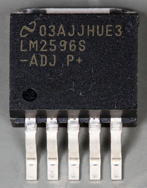
LM2596-ADJ built by National Semiconductor: Step-Down, 1,2V-37V, 3A, 150kHz
Also available with fixed outputs: 3,3V, 5V, 12V


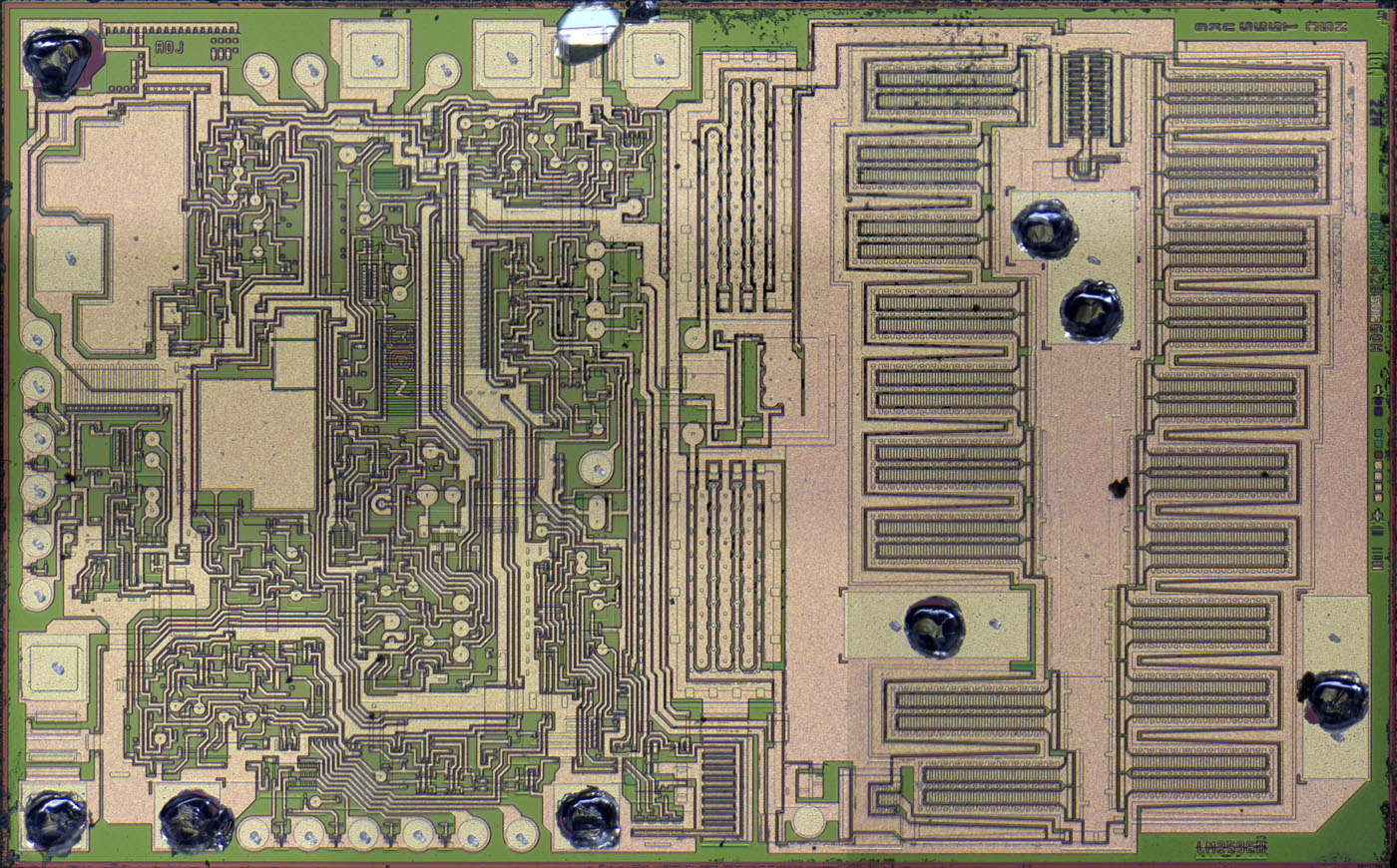
The die is 4,0mm x 2,5mm.
There are a lot of testpads. You also can find four pads that are bigger than the bondpads that were used in this package. Interesting...  :-//
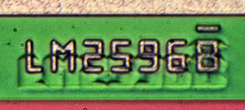


LM2596B
Perhaps B stands for a second revision or it´s the metal layer for the ADJ-regulator.


It´s a 1995 design.


Seven masks, some of them were modified seven times. But perhaps the different output voltages caused some revisions.


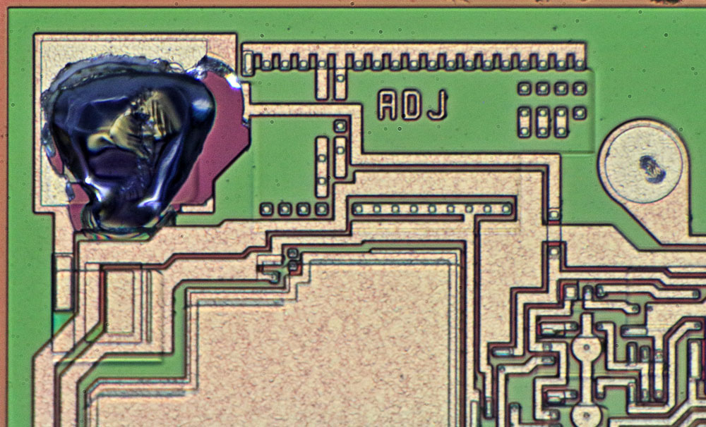
National Semiconductor highlighted the area in which the resistor divider for the voltage feedback is placed with a ADJ. You can see the different contacts of the resistors. In the ADJ-variant no resistor is connected and the potential of the bondpad is routed directly into the regulator.
Unfortunatelly you can´t see the resistors in this die.  :(


That are interesting fusable links! It has to be polysilicon or zener fuse but what does the additional contact above the fuse do?  :-//
Probably the fuses adjust the reference.


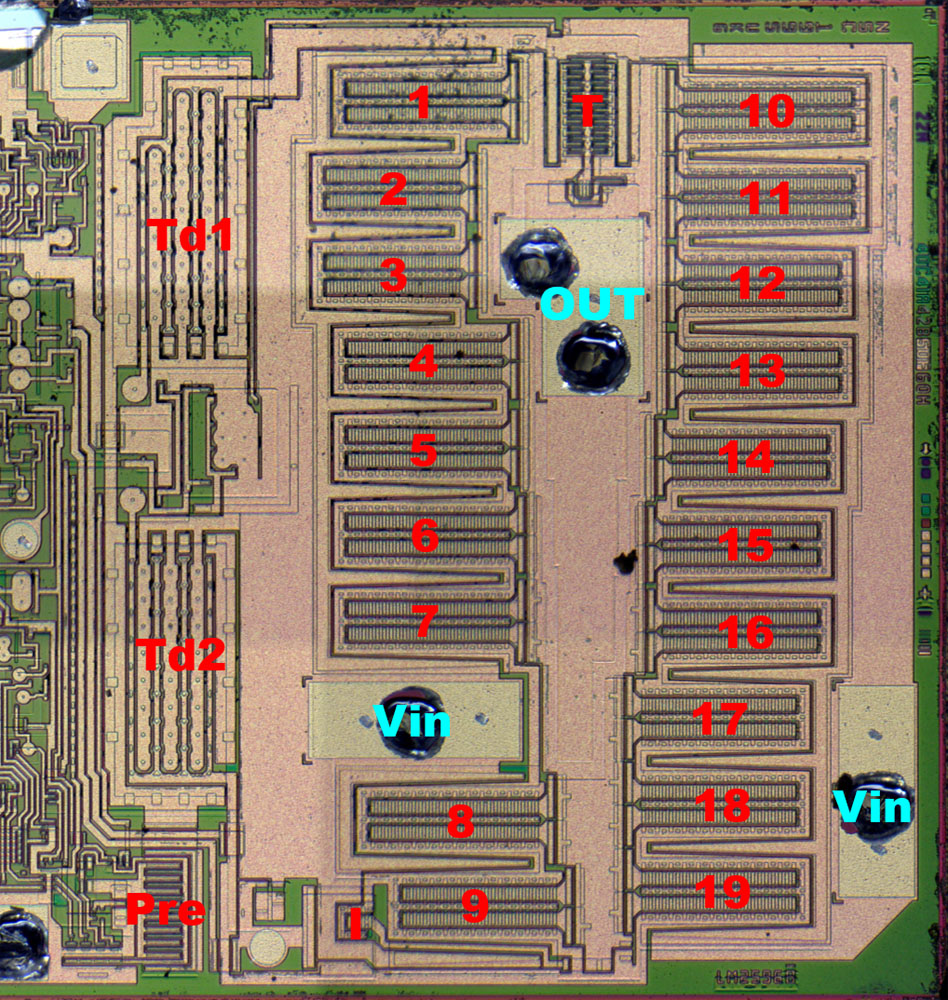
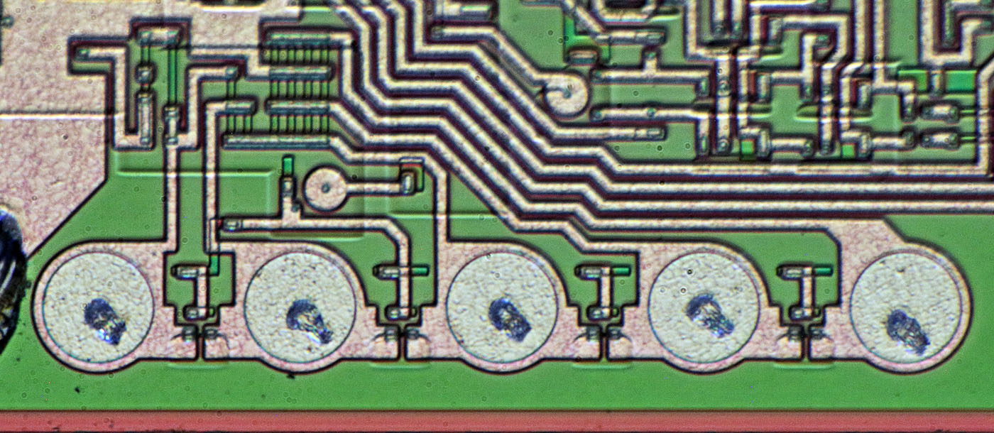
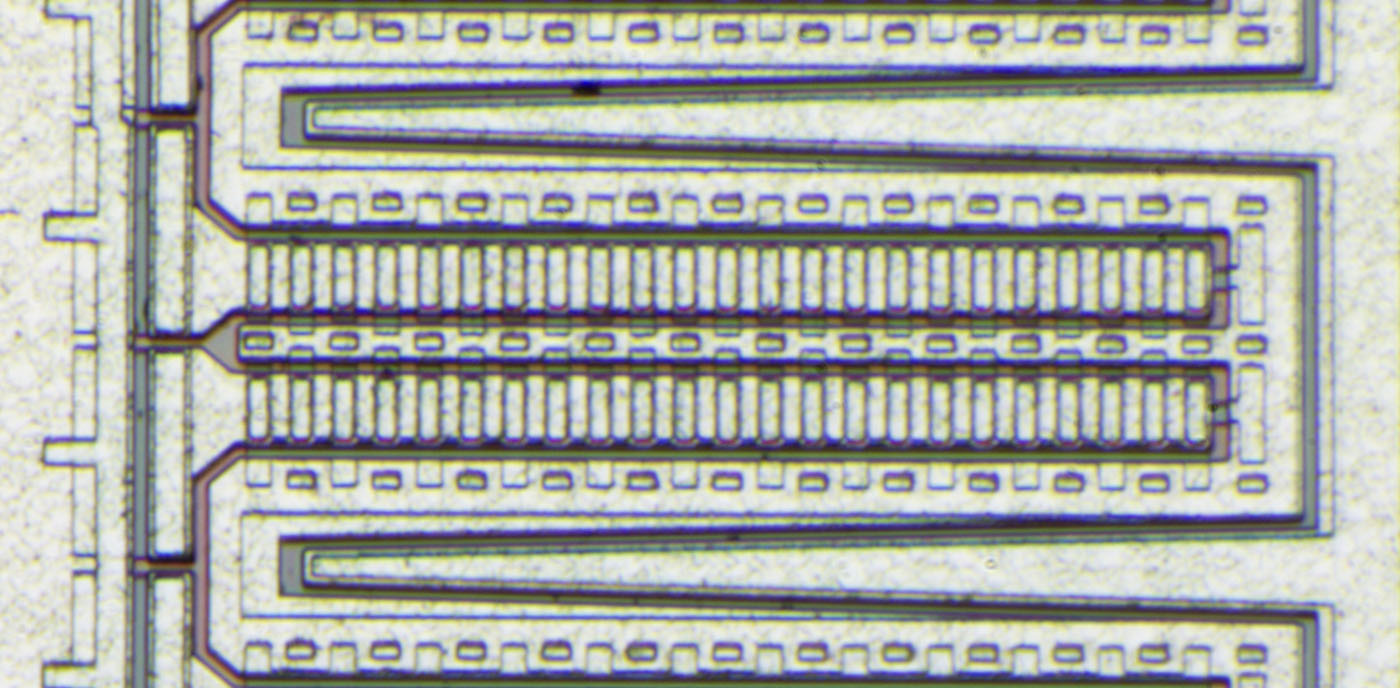
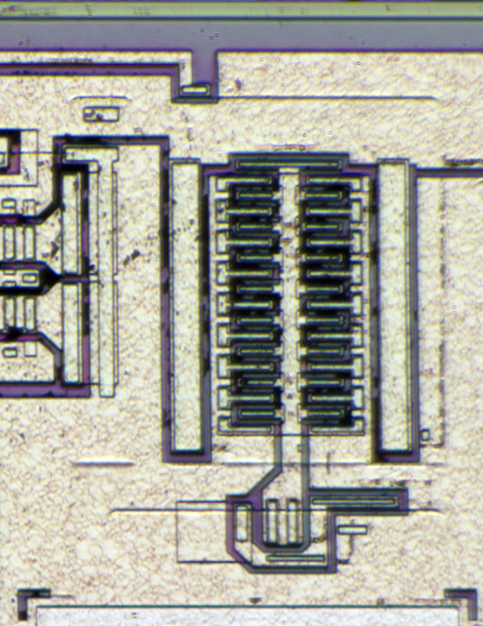
The output stage is a sziklai-transistor with 19 power transistors and two driver PNPs (Td1/Td2).
There is also a small transistor (I) which is used for current sensing.
"Pre" is the driver of the sziklai-transistor.
"T" has to be the temperature sensing element for overtemperature protection.


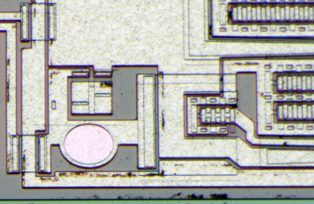
On top of the shunt resistor is a metal square with two slim vias. By moving this vias National was able to adjust the overcurrent threshold.


Big transistor...  :)


I´m not sure but this has to be the overtemperature protection. It seems like the transistor is able to drain the base current of the output transistor.


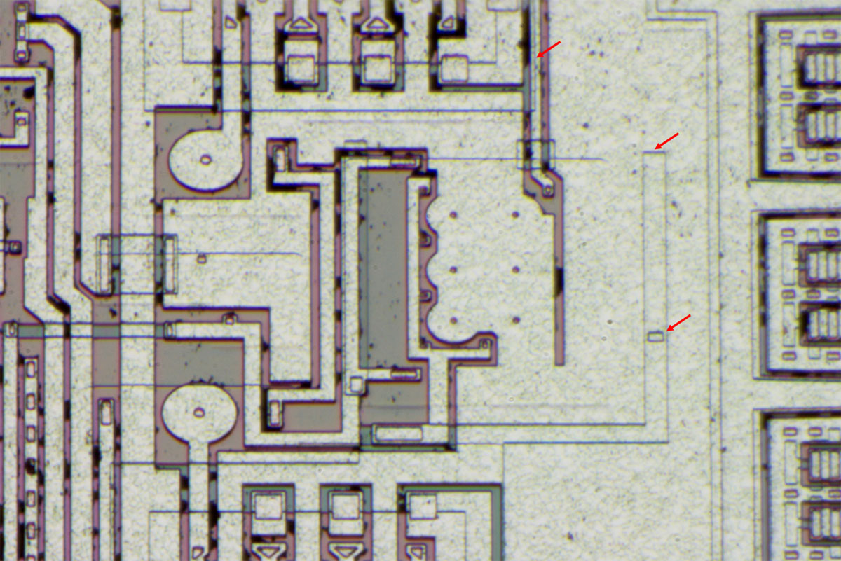
There is one line connecting the "T-area" with a six-PNP-area between the sziklai-drivers.
I´m pretty sure the long resistor connected with one small via gives you the possibility to adjust the overtemperature threshold.


Datasheet: "Self protection features include a two stage frequency reducing current limit for the output switch and an over temperature shutdown for complete protection under fault conditions."
Why reducing the frequency? That sounds not very logical to me.  :-//


Some more pictures:
https://www.richis-lab.de/voltageregulator07.htm

 :-/O
 
The following users thanked this post: Renate

Online David Hess

  • Super Contributor
  • ***
  • Posts: 16613
  • Country: us
  • DavidH
Re: Voltage regulators - die pictures
« Reply #56 on: December 02, 2020, 11:25:54 pm »
That are interesting fusable links! It has to be polysilicon or zener fuse but what does the additional contact above the fuse do?  :-//
Probably the fuses adjust the reference.

Wouldn't zeners be anti-fuses?  I have read that they really do flash when zapped which is to be expected with base-emitter breakdown.

The diagrams I checked show the zener anti-fuse structure inside of an n-well to provide junction isolation so maybe that explains the third connection.
 
The following users thanked this post: Noopy

Offline NoopyTopic starter

  • Super Contributor
  • ***
  • Posts: 1731
  • Country: de
    • Richis-Lab
Re: Voltage regulators - die pictures
« Reply #57 on: December 03, 2020, 05:21:29 am »
That are interesting fusable links! It has to be polysilicon or zener fuse but what does the additional contact above the fuse do?  :-//
Probably the fuses adjust the reference.

Wouldn't zeners be anti-fuses?  I have read that they really do flash when zapped which is to be expected with base-emitter breakdown.

You are right. Of course anti-fuse would be more correct.


The diagrams I checked show the zener anti-fuse structure inside of an n-well to provide junction isolation so maybe that explains the third connection.

Yes! That sounds very reasonable! Thanks!  :-+

Offline NoopyTopic starter

  • Super Contributor
  • ***
  • Posts: 1731
  • Country: de
    • Richis-Lab
Re: Voltage regulators - die pictures
« Reply #58 on: December 04, 2020, 01:35:37 pm »
In comparison to the National Semiconductor LM2596 here we have the STD2596 built by Semtron Microtech:


The die is a lot smaller than the NS LM2596 die: 3,0mm x 1,9mm vs. 4,0mm x 2,5mm. (There is some heat damage on the metal layer.)
You can spot the same big blocks as in the NS LM2596 but everything is a smaller. They have cut the testpads and spare bondpads and the capacitors are smaller. But also the rest of the structures are shrunk.


Semtron Microtech uses normal metal fuses.


The output transistors are quite small.
Although the output transistors are smaller the Sziklai-Driver-Transistors are quite big.
Perhaps the hfe of the output transistors is lower. Perhaps in the used manufacturing process the PNP-transistors didn´t improve as much as the NPN-Transistors.


Look at that: They used perforated emitter transistors as output stage. Probably that´s one reason why they were able to make the die so much smaller.


Some more pictures here:

https://www.richis-lab.de/voltageregulator08.htm

 :-/O

Online David Hess

  • Super Contributor
  • ***
  • Posts: 16613
  • Country: us
  • DavidH
Re: Voltage regulators - die pictures
« Reply #59 on: December 04, 2020, 05:45:24 pm »
The output transistors are quite small.
Although the output transistors are smaller the Sziklai-Driver-Transistors are quite big.
Perhaps the hfe of the output transistors is lower. Perhaps in the used manufacturing process the PNP-transistors didn´t improve as much as the NPN-Transistors.

The higher current density from using smaller output transistors could result in much lower current gain.  One advantage of using larger transistors even when the extra current or power capability is not required is higher current gain.

A larger PNP driver with a smaller lower gain NPN output transistors might still save area for a lower cost design but the higher base current would lower efficiency.

Quote
Look at that: They used perforated emitter transistors as output stage. Probably that´s one reason why they were able to make the die so much smaller.

I am not sure there is any advantage over interdigitated transistors at this scale:

https://www.ti.com/lit/an/snoa661b/snoa661b.pdf?ts=1607103779257
« Last Edit: December 04, 2020, 05:48:45 pm by David Hess »
 
The following users thanked this post: Noopy

Offline Renate

  • Super Contributor
  • ***
  • Posts: 1460
  • Country: us
Re: Voltage regulators - die pictures
« Reply #60 on: December 04, 2020, 05:55:19 pm »
Hmm, so the STD2596 is a newer design than the LM2596?
I was half expecting to see something totally bogus with the STD die.
I'm still at loss how that chip could blow through full input voltage and THEN got back to regulating correctly.
I'm sure it was some strange latch-up mode with a wonky connection on the input.

I guess that if you love something you should put a crowbar on it. >:D
 

Offline NoopyTopic starter

  • Super Contributor
  • ***
  • Posts: 1731
  • Country: de
    • Richis-Lab
Re: Voltage regulators - die pictures
« Reply #61 on: December 04, 2020, 06:43:08 pm »
The higher current density from using smaller output transistors could result in much lower current gain.  One advantage of using larger transistors even when the extra current or power capability is not required is higher current gain.

Of course!  :-+
Absolutely clear!  :-+


Quote
Look at that: They used perforated emitter transistors as output stage. Probably that´s one reason why they were able to make the die so much smaller.

I am not sure there is any advantage over interdigitated transistors at this scale:

https://www.ti.com/lit/an/snoa661b/snoa661b.pdf?ts=1607103779257

Well, I can´t proof it...
I just thought what is good for big power transistors also helps in higher integrated circuits...


Hmm, so the STD2596 is a newer design than the LM2596?

It seems to be newer, yes.


I was half expecting to see something totally bogus with the STD die.
I'm still at loss how that chip could blow through full input voltage and THEN got back to regulating correctly.
I'm sure it was some strange latch-up mode with a wonky connection on the input.

Unfortunately there is no obvious flaw but at least we know now that it is no strange fake chip.  :)

Online David Hess

  • Super Contributor
  • ***
  • Posts: 16613
  • Country: us
  • DavidH
Re: Voltage regulators - die pictures
« Reply #62 on: December 05, 2020, 03:05:27 am »
Unfortunately there is no obvious flaw but at least we know now that it is no strange fake chip.  :)

The damage from excessive heating suggests that the output transistors are too small.
 

Offline NoopyTopic starter

  • Super Contributor
  • ***
  • Posts: 1731
  • Country: de
    • Richis-Lab
Re: Voltage regulators - die pictures
« Reply #63 on: December 05, 2020, 04:12:32 am »
Unfortunately there is no obvious flaw but at least we know now that it is no strange fake chip.  :)

The damage from excessive heating suggests that the output transistors are too small.


Sorry, I wasn´t perfectly clear on this one:
You know I decap the chips by heating the epoxy to above 400°C. Mostly that works quite fine. However the package of the STD2596 was quite hard to crack.  :-// I had to raise the temperature significantly. Unfortunately that damaged the metal layer.

Offline NoopyTopic starter

  • Super Contributor
  • ***
  • Posts: 1731
  • Country: de
    • Richis-Lab
Re: Voltage regulators - die pictures
« Reply #64 on: January 19, 2021, 04:39:42 pm »


I updated the UA732 quite a bit.


Some paint for the schematic. Right now I have no time to translate the whole explanation but you can find quite a bit online and Google Translator is your friend.  ;)


The UA723 and the schematic show the same circuit.  :-+
The output transistor is built with two transistors with emitter resistors for current sharing.


And now lights on!  8)
While operating the two zener diodes are glowing. NICE!  ;D


You even can see how bad the current stability of the J-FET Q1 is. With 30V D1 is a lot brighter than with 15V.
D2 works in the current regulation of the reference circuit and so the current is quite constant.


https://www.richis-lab.de/LM723_06.htm

 :-/O
« Last Edit: January 19, 2021, 04:42:24 pm by Noopy »
 
The following users thanked this post: SeanB

Offline magic

  • Super Contributor
  • ***
  • Posts: 6778
  • Country: pl
Re: Voltage regulators - die pictures
« Reply #65 on: January 19, 2021, 06:25:02 pm »
Nice trick with finding out how bad those JFETs are :-+

There was a whole thread about this chip. And by the way, you posted the incorrect schematic. There is no connection from Q9 and Q11 collectors to VCC ;)
 

Offline NoopyTopic starter

  • Super Contributor
  • ***
  • Posts: 1731
  • Country: de
    • Richis-Lab
Re: Voltage regulators - die pictures
« Reply #66 on: January 19, 2021, 06:32:51 pm »
Nice trick with finding out how bad those JFETs are :-+

There was a whole thread about this chip. And by the way, you posted the incorrect schematic. There is no connection from Q9 and Q11 collectors to VCC ;)


 |O  Thanks for the hint!
That´s the old Fairchild schematic. It looked quite good. Now I have to find the correct one...

It was a long day...


 |O ;D
« Last Edit: January 19, 2021, 06:35:09 pm by Noopy »
 

Offline magic

  • Super Contributor
  • ***
  • Posts: 6778
  • Country: pl
Re: Voltage regulators - die pictures
« Reply #67 on: January 19, 2021, 06:44:01 pm »
Q9 still wrong.

I posted a corrected schematic in the original thread. And TI has a correct one too IIIRC, but it just look ugly :P
Find it and you will see what I mean.
 

Offline NoopyTopic starter

  • Super Contributor
  • ***
  • Posts: 1731
  • Country: de
    • Richis-Lab
Re: Voltage regulators - die pictures
« Reply #68 on: January 19, 2021, 07:29:30 pm »
@all: Sorry for the the first wrong schematic.

@magic: Thanks for correcting me! Certainly you posted the right schematic in the other thread...  :palm:

@all: Sorry for not posting this in the 723-thread... :palm:  I will put a link in the 723-thread...  ;)


This schematic should be correct.

My guess is that the supply of Q9 and Q11 was shifted to isolate them against power supply troubles. In the reference current loop the potentials should be more stable than on V+.  :-/O

Offline NoopyTopic starter

  • Super Contributor
  • ***
  • Posts: 1731
  • Country: de
    • Richis-Lab
Re: Voltage regulators - die pictures
« Reply #69 on: February 05, 2021, 10:52:00 pm »


LNK306, a low cost line voltage regulator.


One pin is missing so the package can withstand the 700V breakdown voltage.


Regulator circuit and power transistor are integrated on one die which is 2,4mm x 1,8mm.


A 2006 design named DS73C.


They didn´t need much rework.


That has to be the feedback pin. ESD protection and overvoltage protection.


Perhaps that´s a bandgap reference and under the metal plate there are the resistors? We don´t know for sure...


That looks like a frequency divider like we have seen it in the Blink-LED (https://www.richis-lab.de/Opto03.htm). There is a restart counter waiting 800ms until restarting the circuit. You can clearly see 13 similar blocks. That gives you 120ms out of the 66kHz. With some more circuitry you get the 800ms.


The upper bondband has to be the Bypass with the zener in the upper right corner.
The lower bondpad has to be the Drain-potential. I´m not 100% sure because it looks like it is connected to the Source but you can´t be sure and that one has to be Drain because the LNK306 is supplied by the Drain and it´s necessary for the overcurrent protection.
The big structure probably is the voltage regulator which has to manage the high voltage and the relatively high power dissipation.


Probably here we see the gate driver.


Power transistor...


The factors of the drain capacitance are interesting. They show us how the smaller regulators are built:


1:2:4 are generated with the upper transistor (purple/green). To built a LNK306 they added a second smaller transistor (red/yellow).
Since the second transistor is smaller but contains the same bondpads the active area is smaller and the factor is not 1:7 but 1:6,8. Nice numbers!  8)


Around the source contact you can see the gate contacts.
The distance between drain an source gives you the necessary voltage rating.


https://www.richis-lab.de/voltageregulator09.htm

 :-/O
 
The following users thanked this post: RoGeorge, Miyuki

Offline NoopyTopic starter

  • Super Contributor
  • ***
  • Posts: 1731
  • Country: de
    • Richis-Lab
Re: Voltage regulators - die pictures
« Reply #70 on: February 15, 2021, 09:38:02 pm »


Maxim MAXM15062, a 500kHz-3,3V-step-down-regulator integrated in a tiny PCB carrying the inductor. You just have to connect the capacitors.


The thickness of the epoxy board is ~240µm. You can see the braided fiberglass in the epoxy. The solder stop mask is ~30µm on each side.


The die is 1,6mm x 1,4mm and is connected like a flip-chip. Between the die and the contacts there is a coating, probably polyimid.
Some contacts are connected to two bondpads.


The die is smaller than the dark rectangle you can see in the PCB. Probably that´s some stuff to secure the die while manufacturing the PCB.


Due to the high temperatures needed to remove the polyimid there is some minor damage on the die.
You can see the big switching transistor and the freewheeling transistor on the left side.


I assume the structures are a little smaller than 1µm.


More pictures here:

https://www.richis-lab.de/voltageregulator10.htm

 :-/O
 
The following users thanked this post: RoGeorge

Offline RoGeorge

  • Super Contributor
  • ***
  • Posts: 6202
  • Country: ro
Re: Voltage regulators - die pictures
« Reply #71 on: February 15, 2021, 09:43:05 pm »
Wow, what a giant battery!   ;D

Offline NoopyTopic starter

  • Super Contributor
  • ***
  • Posts: 1731
  • Country: de
    • Richis-Lab
Re: Voltage regulators - die pictures
« Reply #72 on: February 15, 2021, 09:50:49 pm »
Wow, what a giant battery!   ;D

Indeed!  ;D


I have added the die thickness: a little bit more than 100µm.

Offline NoopyTopic starter

  • Super Contributor
  • ***
  • Posts: 1731
  • Country: de
    • Richis-Lab
Re: Voltage regulators - die pictures
« Reply #73 on: March 19, 2021, 08:27:40 pm »


The famous L200


pink: voltage reference
dark green: current sources
orange/cyan: differential amplifier
purple: overtemperature protection
red: darlington output stage
yellow: SOA-protection, a overcurrent protection with a circuit manipulating the current limit with respect to temperature and voltage drop
green: current regulation comparator
blue: bias circuit for the comparator


The die is 2,2mm x 2,1mm. The circuit matches the schematic.


We know these etch markers and the 8xxx numbers, that´s ST.  :-+


There are two darlington transistors acting as regulator stage.
You can see they are christmas-type transistors with small lines acting as emitter resistors.
On the right side there is the predriver integrated in the collector area of the big transistor.
The metal layer of the upper transistor acts as a shunt resistor. The metal layer of the lower transistor contains a dummy resistor to ensure equal currents.


The voltage reference is integrated at the upper edge of the die so the circuit has the same temperature independent of the load.
R5 has four additional connections so you can adjust the power of the positive tempco that compensates the negative tempco of the reference.


There is a testpad between R16 and R17 to check the overtemperature circuit.


Now that is something you don´t find in the schematic. Around C1 there are six diodes. ...I don´t know why they integrated these diodes...  :-//


https://www.richis-lab.de/voltageregulator11.htm

 :-/O
 
The following users thanked this post: RoGeorge

Offline exe

  • Supporter
  • ****
  • Posts: 2562
  • Country: nl
  • self-educated hobbyist
Re: Voltage regulators - die pictures
« Reply #74 on: March 22, 2021, 10:35:31 am »
The famous L200

Oh, I didn't know it's famous, bumped into it only recently. I bought two before they disappear from sales. My plan is build a circuit with them just for fun.


Share me

Digg  Facebook  SlashDot  Delicious  Technorati  Twitter  Google  Yahoo
Smf