Author Topic: Voltage regulators - die pictures  (Read 30397 times)

exe and 1 Guest are viewing this topic.

Online NoopyTopic starter

  • Super Contributor
  • ***
  • Posts: 1734
  • Country: de
    • Richis-Lab
Re: Voltage regulators - die pictures
« Reply #75 on: March 22, 2021, 12:52:34 pm »
The famous L200

Oh, I didn't know it's famous, bumped into it only recently. I bought two before they disappear from sales. My plan is build a circuit with them just for fun.

Well it was used a lot for current sources like (Pb) battery charger.  :-+

Online NoopyTopic starter

  • Super Contributor
  • ***
  • Posts: 1734
  • Country: de
    • Richis-Lab
Re: Voltage regulators - die pictures
« Reply #76 on: May 19, 2021, 09:11:10 pm »


ST 7824C


The die is 2,1mm x 2,3mm. That´s more than the 1,8mm x 1,8mm of the Siemens TDB7805 (https://www.richis-lab.de/voltageregulator05.htm). The capacitor of the VAS is a lot bigger.


We know these numbers from other ST designs, for example the NE555: https://www.richis-lab.de/555_1.htm
8615 seems to be a process name. L7711 seems to be the name of the design.


And we also know these etch markers from other ST designs.


On the die you can find all the parts that are shown in the schematic in the datasheet. The circuit is quite similar to the Siemens TDB7805.


Two power transistors and two Darlington driver transistors constructed around the big ones.
In one emitter we see the shunt R11 for the current limitation.


A testpad allows to check the overtemperature protection after production.
A small difference to the schematic: The transistor Q14 is driven by an additional driver transistor Q14p.


ST sold variants with output voltages of 5V, 5,2V, 6V, 8V, 8,5V, 9V, 12V, 15V, 18V and 24V. By different connections of the resistors R20a - R20f the resistor divider R20/R19 gives you the feedback signal you need.
While a 7805 guarantees 4,8V - 5,2V the error in a 7824 is multiplied so the output voltage is between 23V and 25V.


Now that is interesting: ST sold two types of the 7800 regulators. 7800 is TO3, 7800C is TO220 or D2PAK.
The 7800 regulator have better specifications (lower noise, lower current consumption,...). But really puzzling is the so called "short circuit current". This current is 0,75A for all the 7800 but gets lower from the 7805C (0,75A) to the 7824C (0,15A). You can´t find an explanation for this in the schematic or on the die.
But let´s look at a teardown Ken Shirriff did (http://www.righto.com/2014/09/reverse-engineering-counterfeit-7805.html). He looked inside a ST 7805 (TO3) and found a circuit that didn´t fit to the schematic in the datasheet. There is the assumption that the circuit was designed by Thomson. It seems like ST packaged one (the older) circuit in the TO3 and the TO220 and D2PAK got the other circuit. That would explain the different specifications and the different short circuit current behaviour.


https://www.richis-lab.de/voltageregulator12.htm

 :-/O
 
The following users thanked this post: exe, RoGeorge

Offline amishasingh

  • Contributor
  • !
  • Posts: 17
  • Country: ca
Re: Voltage regulators - die pictures
« Reply #77 on: May 20, 2021, 12:22:20 pm »
Looks cool and informative related to the voltage regulators ⚡⚡⚡
Amisha
 

Online NoopyTopic starter

  • Super Contributor
  • ***
  • Posts: 1734
  • Country: de
    • Richis-Lab
Re: Voltage regulators - die pictures
« Reply #78 on: May 29, 2021, 06:56:08 pm »


7812 built by Mikroelektronika Botevgrad, the company which had built the Apple II clones in soviet times: https://www.richis-lab.de/prawez.htm


Hey, we know this design! It´s a ST 7812: https://www.richis-lab.de/voltageregulator12.htm
The die was potted in some jelly.


The voltage divider was modified to get 12V and the metal layer shows the appropriate 12.


https://www.richis-lab.de/voltageregulator13.htm

 :-/O
 
The following users thanked this post: RoGeorge

Online NoopyTopic starter

  • Super Contributor
  • ***
  • Posts: 1734
  • Country: de
    • Richis-Lab
Re: Voltage regulators - die pictures
« Reply #79 on: July 04, 2021, 08:29:13 pm »


Here we have a Flyback Controller with integrated power transistor: Power Integrations TOP250
In an open frame supply the TOP250 can deliver 290W.


The die is 5,4mm x 4,0mm with a huge power transistor.


The control circuit is a bit bigger than the control circuit of the LNK306 we have seen here: https://www.eevblog.com/forum/projects/voltage-regulators-die-pictures/msg3450066/#msg3450066


Designed in the year 2000 it seems like the first revision was ok (eight 0 for eight masks).


Besides the gate connection there is an additional wire leading from the control circuit to the power transistors near the source contact. The datasheet shows that the current measurement works with the drain potential. Perhaps actually the current is measured at the source contact...


There are nine versions of the flyback controller with different current ratings. Probably the transistor area is changed to get the different versions. The number of the transistor segments (27) fits nearly perfect to the factor of the different current limits (14)


https://www.richis-lab.de/voltageregulator14.htm

 :-/O
 
The following users thanked this post: RoGeorge, Miyuki

Online exe

  • Supporter
  • ****
  • Posts: 2563
  • Country: nl
  • self-educated hobbyist
Re: Voltage regulators - die pictures
« Reply #80 on: July 04, 2021, 09:20:55 pm »
Concerning the transistor, it's a mosfet, but its labyrinth-like structure resembles a bjt to me. Kinda weird...
 

Online NoopyTopic starter

  • Super Contributor
  • ***
  • Posts: 1734
  • Country: de
    • Richis-Lab
Re: Voltage regulators - die pictures
« Reply #81 on: July 05, 2021, 03:57:24 am »
Concerning the transistor, it's a mosfet, but its labyrinth-like structure resembles a bjt to me. Kinda weird...

These structures are often confusing.  :-+

Online NoopyTopic starter

  • Super Contributor
  • ***
  • Posts: 1734
  • Country: de
    • Richis-Lab
Re: Voltage regulators - die pictures
« Reply #82 on: September 30, 2021, 08:51:19 pm »


LM2576, a buck converter switching with 52kHz for load currents up to 3A generating 1,23V to 37V. The HV version can supply you with up to 57V.


The die is 3,8m x 2,5mm.
It is quite similar to the LM2596 (https://www.richis-lab.de/voltageregulator07.htm).


JDC? A National Semiconductor branch?
K.H, HIDE? Some enigneers?
LM1576 is the version specified for a temperature range from -55°C to +150°C.
This is the ADJ version. There are also fixed voltage versions.


NSUK? National Semiconductor United Kingdom?


The green areas contain the power transistors. The yellow area is the driver. The red area can drain the base current of the power transistors. The single cyan transistor is used to measure the output current with the blue elements.


12 segments with 3 lines with 7 transistors


The emitter resistors have different lengths to adjust the current distribution over the individual transistor lines.


The driver transistor is a PNP. The whole output stage is a Sziklai-stage.


That is the transistor sinking the base current of the power transistor at too high temperatures or currents.


The single transistor is not directly connected to the output. The resistor Rs is the shunt resistor. The resistors Ra and Rb connect the shunt to a differential amp. You can adjust Rs and Ra a little by moving the two vias where the two are connected to each other. You can adjust Ra a lot by connecting the contacts ADJ and by connecting the right ADJ contact to the differential amp over the short metal line that is totally disconnected here.


In the upper area we have the driver for the Sziklai pair. The current of the PNP driver transistor is fed to an exclusive bondpad.


control circuit


Here we have the bandgap reference. Red is the current mirror, cyan and green are the two transistors with an ratio of 6:1. On the right side there are the resistors of the bandpag reference. By adjusting the resistors with the testpads and the fusible links you can adjust the temperature coefficient.


Here we see the voltage divider of the feedback. By connecting the resistors in different ways you get different fixed voltages.


The testpads and fusible links at the bottom of the die are probably used to adjust the output voltage.


A second LM2576 looks a little different. (Actually it was the first one.  ;D)


The die is quite similar (and damaged).


But here we have NSTE instead of NSUK. National Semiconductor TExas?  :-//


https://www.richis-lab.de/voltageregulator15.htm

 :-/O
 
The following users thanked this post: exe, RoGeorge

Offline ElBenjo

  • Contributor
  • Posts: 10
  • Country: mx
Re: Voltage regulators - die pictures
« Reply #83 on: March 25, 2022, 10:44:53 pm »
Hello. This is my first post in this forum, and I know this is an old post but I think is the right place for this. More than 10 years ago I found a bunch of the component that you see in this picture. Unfortunately, couldn't found any information about this particular IC. Someone recognize it?

" alt="" class="bbc_img" />

At first, I tought it was a transistor, but then I opened and found the chip you see in this picture. Than made me think it is a voltage regulator.

" alt="" class="bbc_img" />

For comparison the third picture show a UA7812C regulator die next to it.

" alt="" class="bbc_img" />
« Last Edit: March 25, 2022, 10:49:07 pm by ElBenjo »
 

Online NoopyTopic starter

  • Super Contributor
  • ***
  • Posts: 1734
  • Country: de
    • Richis-Lab
Re: Voltage regulators - die pictures
« Reply #84 on: March 26, 2022, 09:03:59 am »
Sorry, I have no clue...  :-//

Looks quite big...

Offline ElBenjo

  • Contributor
  • Posts: 10
  • Country: mx
Re: Voltage regulators - die pictures
« Reply #85 on: March 27, 2022, 06:06:31 am »
Yes, it is big. I tested it with one of those cheap component testers and it marks it as a pnp transistor with a 1.3 voltage drop and hfe = 0. I supposed it was a Darlignton transistor but in the breadboard I couldn't make it work as a transistor (and the die shows it is not). I'll try to make it work as a voltage regulator and see what voltage I get at the output.
 

Online NoopyTopic starter

  • Super Contributor
  • ***
  • Posts: 1734
  • Country: de
    • Richis-Lab
Re: Voltage regulators - die pictures
« Reply #86 on: March 27, 2022, 06:12:15 am »
Perhaps a closer look would reveal who designed it and for what purpose.
If you want to send it to Germany...  :-/O

Offline SeanB

  • Super Contributor
  • ***
  • Posts: 16284
  • Country: za
Re: Voltage regulators - die pictures
« Reply #87 on: March 28, 2022, 07:19:03 am »
Perhaps an automotive low side driver, or an intelligent power driver of some sort.
 

Offline ElBenjo

  • Contributor
  • Posts: 10
  • Country: mx
Re: Voltage regulators - die pictures
« Reply #88 on: March 31, 2022, 04:51:01 am »
I made some tests connected as a voltage regulator and what I get is that the output voltage is equal the input voltage when the voltage is less than about 15v, otherwise the output is 0v. So, I guess is an IC like the RBO40.


Online NoopyTopic starter

  • Super Contributor
  • ***
  • Posts: 1734
  • Country: de
    • Richis-Lab
Re: Voltage regulators - die pictures
« Reply #89 on: March 31, 2022, 05:21:22 am »
But a RBO40 would just clamp the voltage not cut it down to 0V.  ???

I haven´t seen an open RBO40 yet but I would suspect it is built with some high-power devices, not with a complex integrated circuit.

Offline ElBenjo

  • Contributor
  • Posts: 10
  • Country: mx
Re: Voltage regulators - die pictures
« Reply #90 on: April 01, 2022, 05:33:33 am »
Sorry, I'd wanted to say that it's function looks similar to an RBO40. I'm still looking if I can find the exact part datasheet.
 

Offline oz2cpu

  • Frequent Contributor
  • **
  • Posts: 850
  • Country: dk
    • webx.dk private hobby and diy stuff
Re: Voltage regulators - die pictures
« Reply #91 on: April 01, 2022, 09:30:57 am »
am i the only one who envy the optical capabilities of your microscope and camera setup ?
WOW those pictures are just amazingly great.
Radioamateur OZ2CPU, Senior EE at Prevas
EMC RF SMPS SI PCB LAYOUT and all that stuff.
 

Online NoopyTopic starter

  • Super Contributor
  • ***
  • Posts: 1734
  • Country: de
    • Richis-Lab
Re: Voltage regulators - die pictures
« Reply #92 on: April 01, 2022, 01:27:07 pm »
Thanks!

I´m doing my very best and still have a lot of pictures to upload...  8)
...and I have even more parts in my inbox and on my ToDo list.  ;D
 
The following users thanked this post: oz2cpu

Online NoopyTopic starter

  • Super Contributor
  • ***
  • Posts: 1734
  • Country: de
    • Richis-Lab
Re: Voltage regulators - die pictures
« Reply #93 on: April 19, 2022, 06:31:39 pm »


Tesla MA7805, another 78xx voltage regulator.

9321 is not the datecode. WN stands for November 1988.


The schematic in the datasheet looks similar to the schematic of the Siemens TDB7805 (https://www.richis-lab.de/voltageregulator16.htm).


NICE!  8)


The die is 2,2mm x 2,3mm. It´s a different design compared to the Siemens, the ST Microelectronics and the Mikroelektronika Botevgrad 78xx regulator. Nevertheless, the main parts look quite similar.

There are a lot of options to tune the circuit by a small change in the metal layer.


MA7805  :-+

The NEF perhaps stands for a manufacturing process. In the MAX199 (https://www.richis-lab.de/REF02a.htm) there were the letters NDE.
(Aside from that the N is really strange...)

The big and small rectangles make it possible to check the alignment of the masks. And we have the Logo you can find in every Tesla ICs.


Here we have the mask revisions: 1A, 2A, 3A, 4C, 5B, 6C, 7C, 8A.

I don´t know what 140 should tell us.


Contrary to the other 78xx regulators in the MA7805 the current flows from left to right.

In the upper left corner you can adjust the SOA-limit. In the upper right corner you can adjust the current limit.


The contact wires of the driver transistors are getting thinner and thicker relative to the current they have to conduct.


In the middle of the die you can adjust the temperature derating. In the lower part you can adjust the voltage reference.


And here we have the area to adjust the output voltage. In the MA7805 we just have the 5kΩ pull-down resistor. The other resistors can be used to build the voltage divider to get higher voltages.


https://www.richis-lab.de/voltageregulator16.htm

 
The following users thanked this post: SeanB, RoGeorge, floobydust, Miyuki

Online NoopyTopic starter

  • Super Contributor
  • ***
  • Posts: 1734
  • Country: de
    • Richis-Lab
Re: Voltage regulators - die pictures
« Reply #94 on: August 05, 2022, 07:15:46 pm »


The B260 is a switching regulator from the "Halbleiterwerk Frankfurt Oder". W3 stands for a production in March 1988.


The datasheet of the B260 contains a block diagram. The B260 is similar to the TDA1060. It is a classic simple design for a switching controller.


A more detailed schematic of the B260 is shown in the magazine "Radio Fernsehen Elektronik" in February 1982.


The die of the B260 is placed on a solid metal carrier, which improves cooling by heat spreading. We have seen this in the U82720 too (https://www.richis-lab.de/GraKa04.htm).


The die is 2,7mm x 2,1mm.


The component name is integrated on the die. The numbers 04 most likely stand for a fourth generation of the switching regulator.


The masks used show the number 1 eight times. This seems to be the first revision of this generation.


The bonpads can be assigned to the pins quite easily. The bondpad of pin 1 is marked by cut corners at the lower edge.


The Brokaw bandgap reference voltage source is clearly visible. The function of such a reference voltage source is described in more detail in the context of the TL7705A voltage monitor (https://www.richis-lab.de/TL7705.htm). Two transistors with an emitter area ratio of 7:1 (blue) operate with a total of three emitter resistors (green). The reference voltage can be tapped at the test point Ubg. A voltage divider (yellow) sets the desired output voltage of the reference voltage source. In the upper right area of the picture there is a current mirror (white) which supplies the two transistors.


The output transistor is located in the upper left corner of the die. Two diodes have been integrated in the supply line, not just one as shown in the schematic.


The resistor at pin 7 and the capacitor at pin 8 are used to set the clock frequency of the B260. The block R7, T7, D7 T8 represents a current source which charges the capacitor C8. R7 defines the current value. Transistor T7 has six emitter areas, only two of which are contacted. The number of contacted emitter areas can be used to preset the strength of the current source. This can be advantageous if the specs of the integrated transistors are not yet known exactly.

Transistor T9 switches on at a certain potential at capacitor C8 and thus discharges it to a lower threshold at which T9 switches off again. The output transistor is controlled in parallel via transistor T10.


https://www.richis-lab.de/voltageregulator17.htm

 :-/O
 
The following users thanked this post: SeanB, RoGeorge

Online NoopyTopic starter

  • Super Contributor
  • ***
  • Posts: 1734
  • Country: de
    • Richis-Lab
Re: Voltage regulators - die pictures
« Reply #95 on: August 26, 2022, 09:31:31 pm »


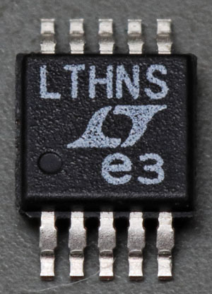
The Linear Technology LT3750 is a switching regulator in an MSOP package. The device is specialized to charge a capacitor to a high voltage. The datasheet lists warning lights, photo flashes, security systems, high voltage sources, electric fences and igniters as possible applications.


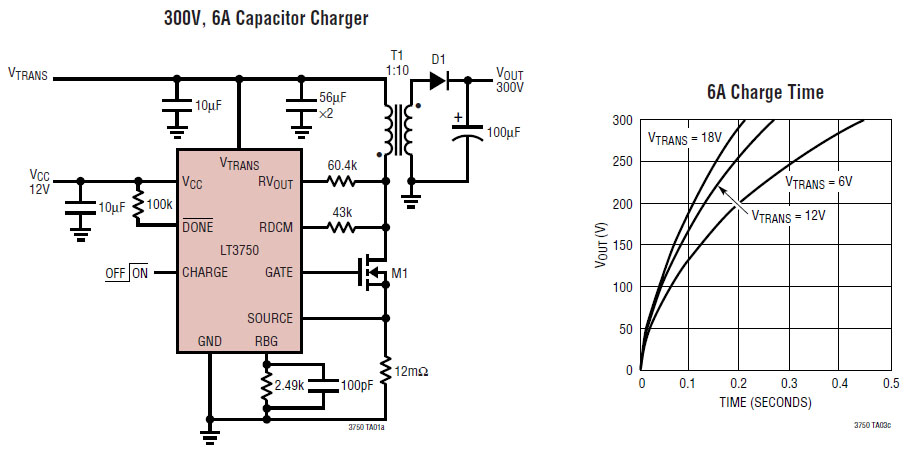
An application example in the datasheet charges a 100µF capacitor to 300V in half a second. It is basically just a flyback converter with a primary side measurement of the secondary voltage. However, the regulator is optimized to charge a capacitor. The datasheet refers to patents 6518733 and 6636021 but these do not describe exactly how the LT3750 works.


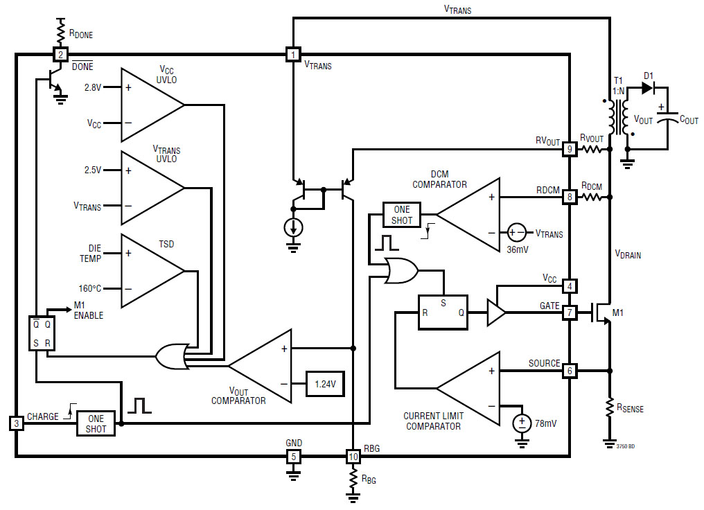
The block diagram in the datasheet shows the operation of the controller. Pulling pin 3 high generates a pulse which enables the control of the power transistor M1 via the left flip-flop and switches the power transistor on at the same time via the right flip-flop. As a result the current through the transformer increases linearly to the limit set by the resistor Rsense. The current limit comparator then ensures that the power transistor is switched off again via the right flip-flop.

The energy stored in the transformer as a magnetic field charges the capacitor Cout via the diode D1 in the blocking phase. In this phase the voltage of the secondary is transferred to the primary in proportion to the turns ratio. When the current flow ends the voltage at the power transistor drops again to the supply voltage Vtrans, whereupon the DCM comparator again activates the right flip-flop and thus the power transistor. The switching frequency ranges between 100kHz and 300kHz.

The secondary voltage transformed to the primary side is monitored via pin RVout. For this purpose the resistor RVout generates with the internal current mirror a current proportional to the transformed voltage. The current mirror is not used in this circuit to simply duplicate a current. It ensures that resistor RVout operates with Vtrans as the reference potential. Thus, the current through resistor RVout becomes independent of the supply voltage of the primary side and is only proportional to the transformed secondary voltage. Equally advantageous the potential at the upper contact of resistor Rbg is independent of the potentials at Vtrans and RVout. The voltage drop across Rbg, proportional to the secondary voltage, switches the Vout comparator when the desired secondary voltage is reached. As a result, the left flip-flop is reset and the Done output signals that charging is complete.

Three other comparators serve as protection circuits and can abort the charging process. Abort occurs when the temperature exceeds 160°C and when the supply voltages drop below 2,5V and 2,8V respectively. The usefulness of the Vcc lower limit is questionable, since the output voltage of the gate driver can already drop to 3V at a supply voltage of 5V. Unfavorably, the Done output is also activated in the error state, suggesting that the charging process was successful.  :o

The primary side measurement of the secondary voltage is particularly advantageous here because a voltage divider on the secondary side would discharge the capacitor. However, many flyback regulators are capable of this primary-side measurement. The LT3750 has the additional advantage that it is optimized for charging an empty capacitor once. It does not need to regulate the secondary voltage, but permanently transfers the same energy packets and deactivates when the desired voltage is reached. This process can be better optimized for minimum charging time than an ordinary regulation. Switching off the regulator may cause a drop in the secondary voltage but this avoids a prolonged dwell in inefficient operating points.


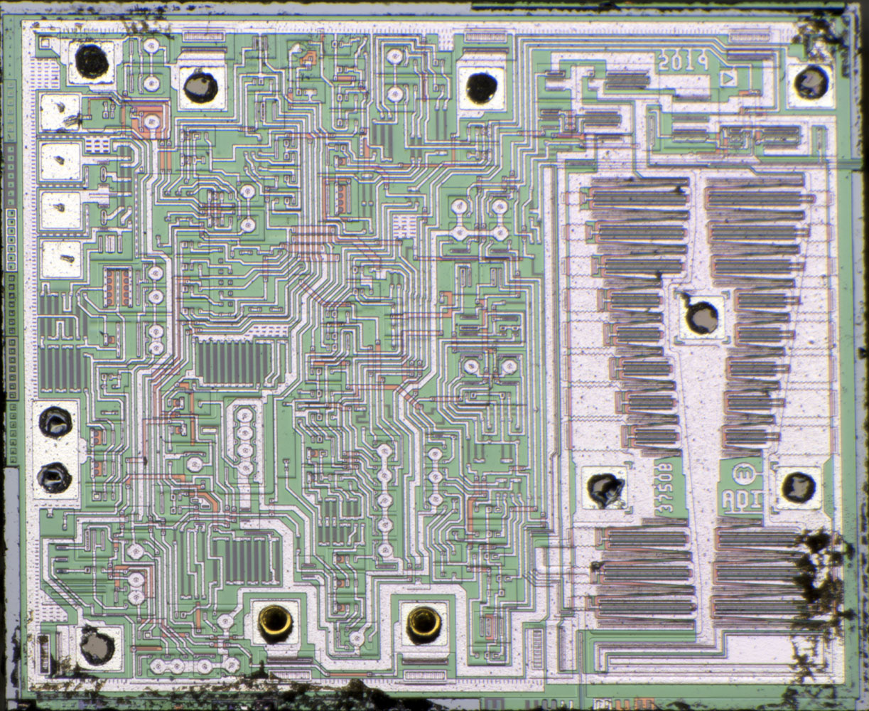
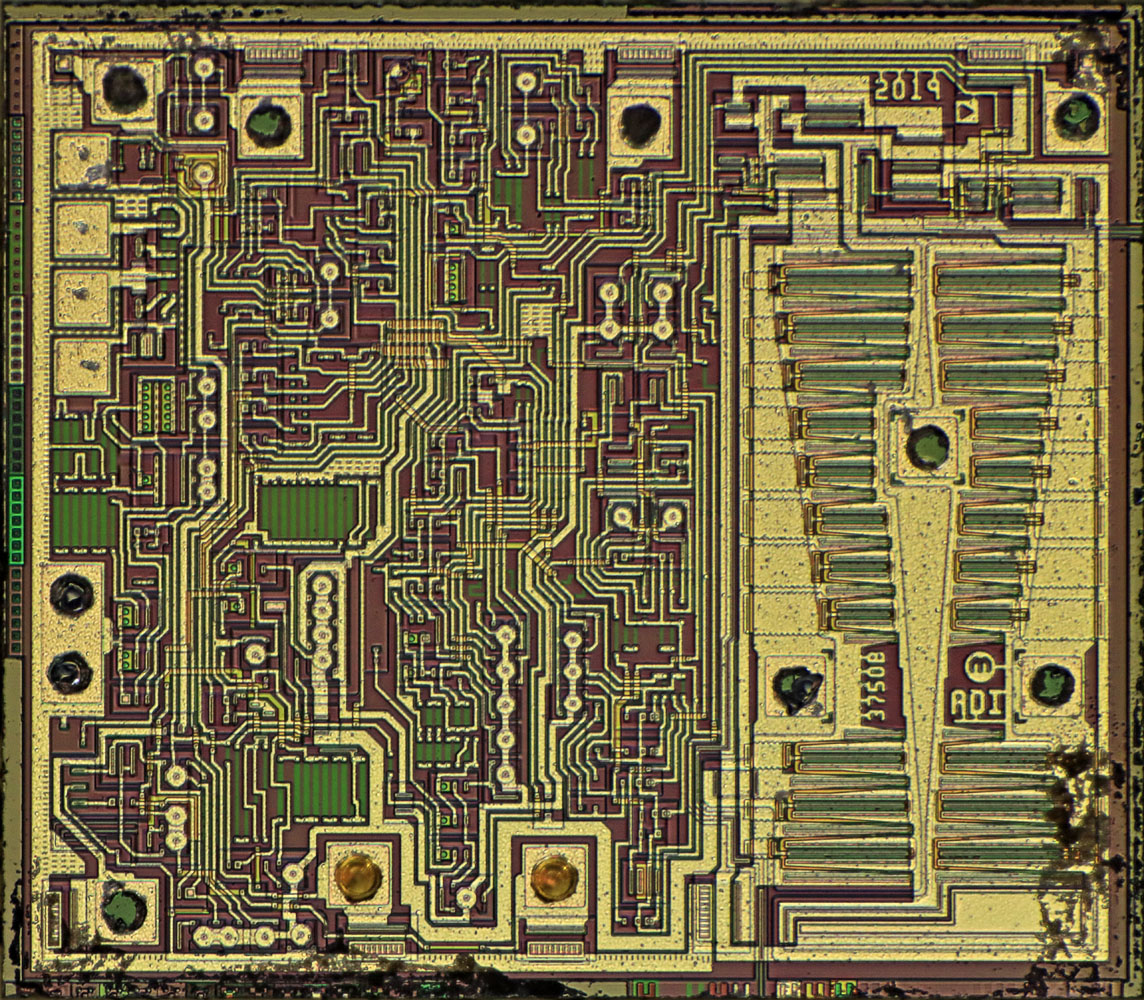
The die is 1,6mm x 1,4mm in size. The large transistors of the driver stage are clearly visible in the right area. The remaining elements are also still quite clear. It would be quite possible to analyze the circuit completely.


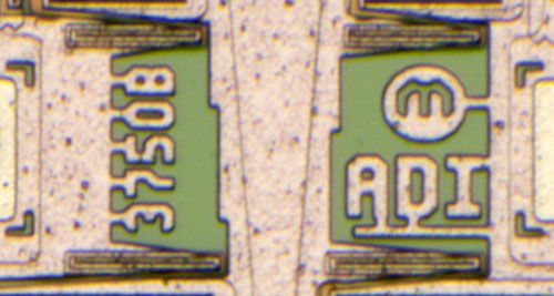
The LT3750 was developed by Linear Technology. However the abbreviation ADI shows that the design has been revised by Analog Devices in the meantime. The B at the end of the designation 3750B probably stands for a second revision.


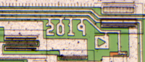
On the edge there are some patterns that allow to check the alignment of the masks against each other.


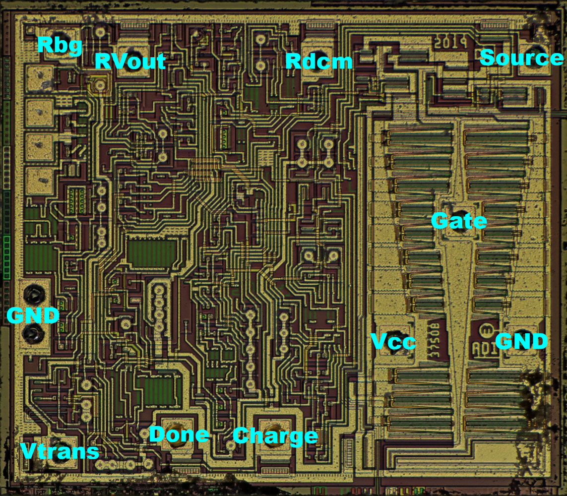
The bondpads can be assigned to the pins of the module relatively unproblematic. The ground potential contacts the device twice, once in the control area and once at the driver transistors.


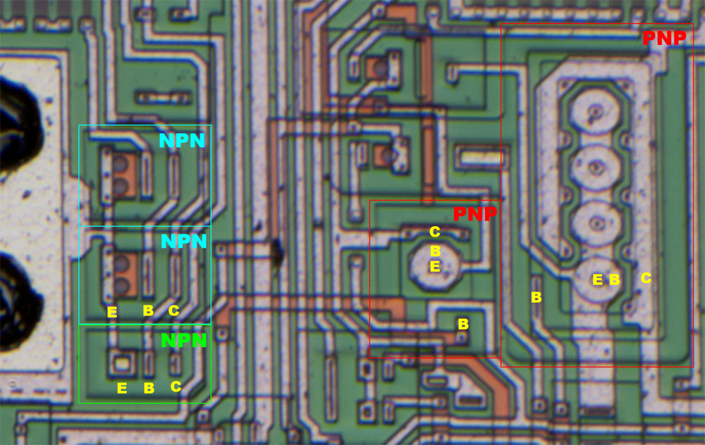
The PNP transistors (red) of the integrated circuit have the usual round structures, where the emitters are located inside. Around the emitter the collector is integrated. Both are separated by a base ring, which is contacted slightly outside.

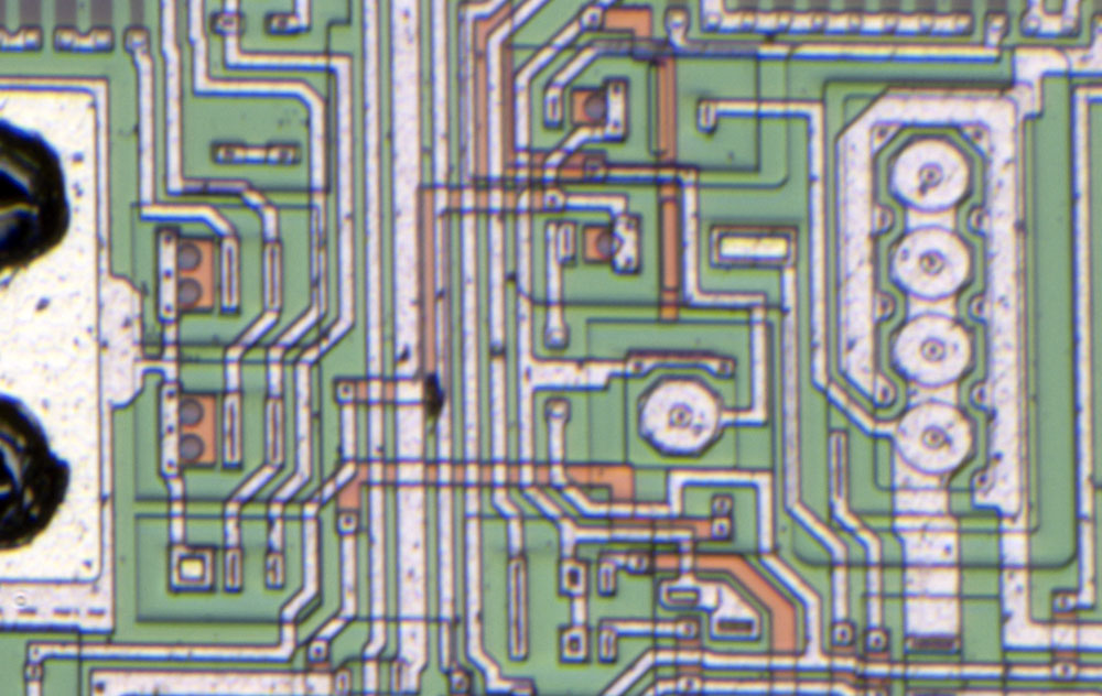
There are also the usual NPN transistors (green). One thinks to be able to recognize the outlines of a buried collector supply line. The base area is also not visible in color, but can be guessed by the contours, just like the emitter.

Besides the usual NPN transistors there are other, very strange NPN transistors (cyan). Their emitter consists of an orange area with one or more dark circles. The contacting of the emitter apparently takes place in the orange area. Since the orange material is also used as a conductor it must be highly doped. It seems most likely that the orange material is heavily n-doped and the dark circles are even slightly more heavily n-doped. It may also be that they are just dimples. It could be that this generates a low-lying base-emitter interface, similar to a buried Zener diode.
 :-//


In the upper left area of the die (here rotated by 90°) are four testpads. The many resistors to the right of the testpads and the two very differently sized transistors above them are reminiscent of a bandgap reference voltage source. However, if you analyze the circuitry, you can see that the current sink of the current mirror is located in this area. The current mirror itself is built with three PNP transistors, which are located on the left between the bond pads Rbg and RVout. The current value in the reference path of the current mirror should not be too critical. However, the current sink also determines the switching threshold of the Vout comparator and this threshold should be hit reasonably accurately for all devices, for which an adjustment makes absolute sense.


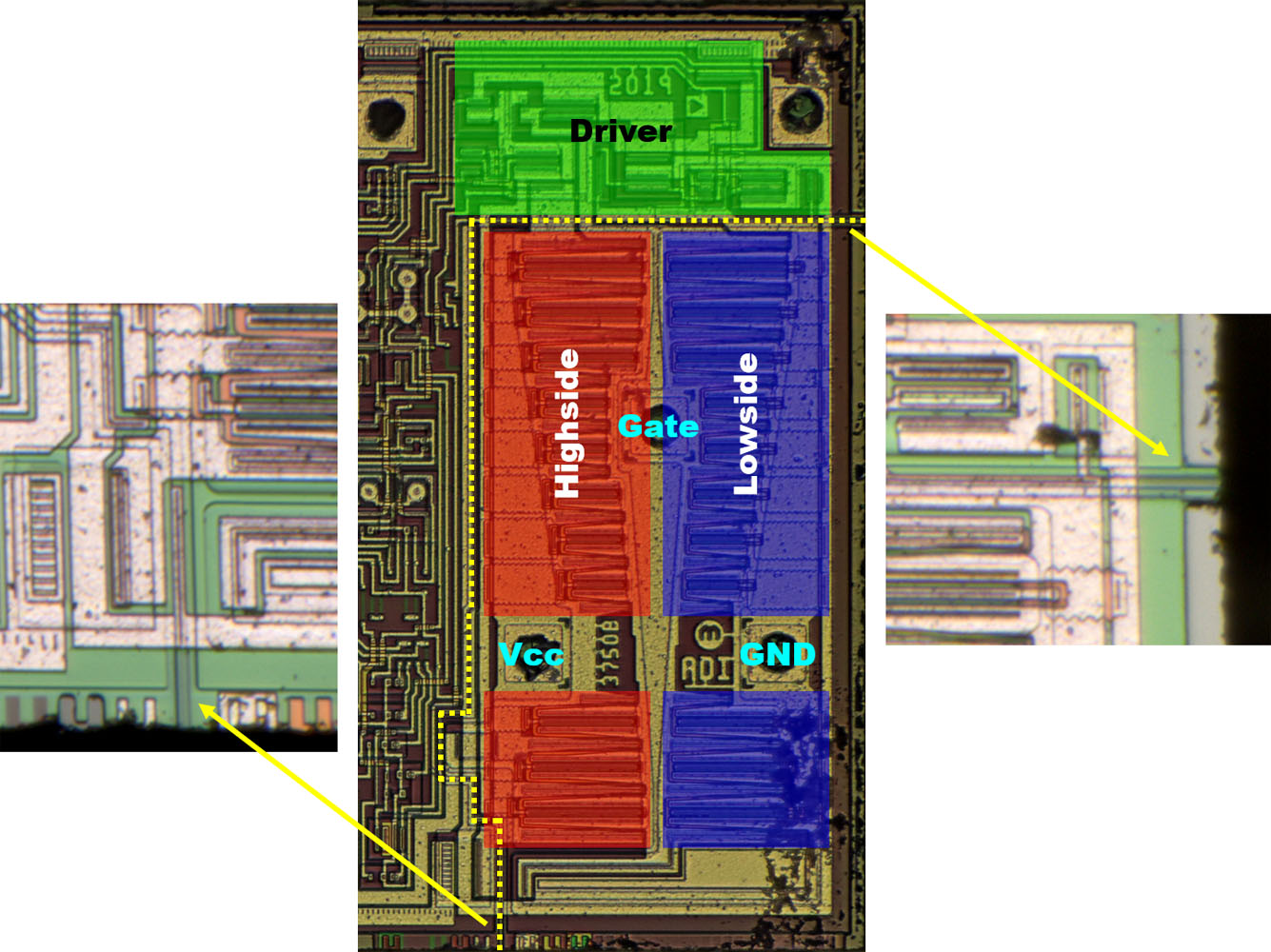
The gate driver consists of a highside and a lowside transistor (red/blue). Above this are the drivers for this push-pull stage (green). The gate driver area is isolated from the rest of the circuit (yellow), which presumably is done to reduce interfering feedback.


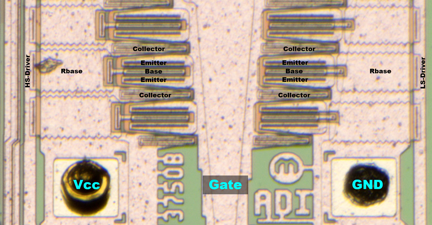
The details show that the output stage transistors have an unusual structure. Both Lowside and Highside contain NPN transistors. However, the base terminal is located in the center and is surrounded by two emitter contacts. The emitter is shaped like a ring.

Also unusual is the large area resistor. One would expect emitter resistors, which provide an even current distribution. However, the resistors are located at the base connections. The current distribution could be influenced in this way, but only as long as the transistors are not operated in saturation, which is certainly the case here. In addition, the control of the emitter current via the base resistors would be subject to very large fluctuations. As will be shown in a moment, there is even more to be said for the fact that these are not measures for uniform current distribution. This means that the individual transistors are constructed in such a way that the current is distributed sufficiently evenly even without balancing resistors.


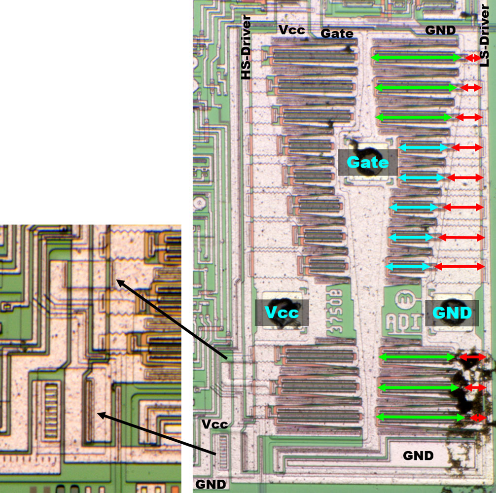
The lines of the potentials Vcc, Gate and GND are designed in such a way that they become wider according to the increasing current load. At first glance, one gets the impression that different transistor sizes have been deliberately integrated here (green/cyan), but in fact one has merely filled in the areas that resulted between the necessary trace widths.

In this context no meaningful correlation between the length of the base resistor and the remaining conditions can be seen. In combination with the very wide design and the use of heavily doped areas, it can be assumed that the strips merely serve as an undercrossing of the metal layer and that their resistance is more of a parasitic property.

The ground potential is connected to the base of the gate driver at the bottom right. It also represents a kind of screen at the left edge. The Vcc potential is led out to the left in the lower area and used to power the rest of the circuit. At the lower edge an element connects Vcc and GND. This could be a Z-diode that dissipates overvoltages. The highside and lowside transistors are controlled from above.


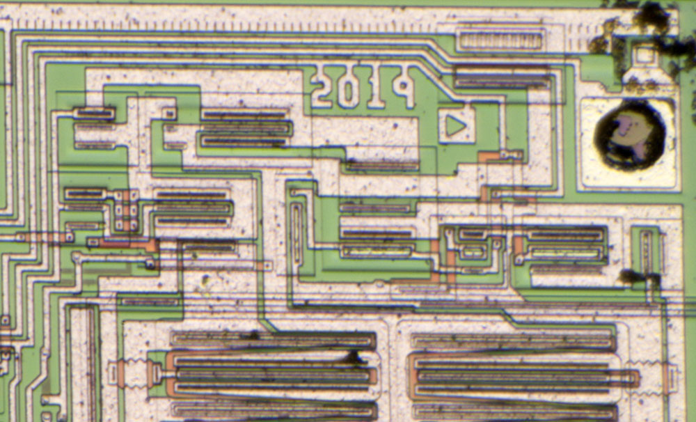
The circuit for controlling the gate driver is located on the upper edge of the die.


https://www.richis-lab.de/voltageregulator18.htm

 :-/O
 
The following users thanked this post: RoGeorge

Offline magic

  • Super Contributor
  • ***
  • Posts: 6779
  • Country: pl
Re: Voltage regulators - die pictures
« Reply #96 on: August 27, 2022, 07:00:29 am »
This looks like that crazy BiCMOS stuff, where they use CMOS technologies to fabricate bipolar transistors. One such classic CMOS process step is deposition of doped polycrystalline silicon over a layer of oxide to fabricate CMOS gates (and an additional layer of interconnects which comes almost for free).

In BiCMOS, the poly layer can be used to fabricate poly-emitter NPNs: a hole is etched in the insulating layer, and N-doped polysilicon is deposited right on the base, forming the emitter. I suppose it ends up being cheaper than adding a traditional emitter diffusion step to CMOS. I seem to recall that poly-emitters are even supposed to have some additional advantages at high frequencies, so they end up used in high performance pure-bipolar processes. Maybe mawyat could tell you more, or call me out for being full of it ;)

It's possible that the transistor you marked in green uses the same emitter construction, but it's hidden under metal so you don't see it. Maybe HF/HCl could reveal something interesting.

Some links about BiCMOS fabrication:
https://www.iue.tuwien.ac.at/phd/puchner/node48_app.html
https://www.maximintegrated.com/en/qa/reliability/general/

Maxim's SG processes appear to be capable of complementary bipolar, but that part isn't shown there. MAX6350 is fabbed on SG3.
 
The following users thanked this post: Noopy

Online NoopyTopic starter

  • Super Contributor
  • ***
  • Posts: 1734
  • Country: de
    • Richis-Lab
Re: Voltage regulators - die pictures
« Reply #97 on: August 27, 2022, 01:43:05 pm »
In BiCMOS, the poly layer can be used to fabricate poly-emitter NPNs: a hole is etched in the insulating layer, and N-doped polysilicon is deposited right on the base, forming the emitter.

That´s a possible explantion.  :-+


But it´s still strange there are normal NPN transistors too.
I somehow don´t believe the green NPNs are the same as the cyan ones and they just connected them with a rectangular massive metal plate. I´m sure it was important for them to connect the orange area and not the dark areas.  :-//

As soon as I have my acids working for me again I will try to look under the metal.

Offline magic

  • Super Contributor
  • ***
  • Posts: 6779
  • Country: pl
Re: Voltage regulators - die pictures
« Reply #98 on: August 27, 2022, 03:05:35 pm »
The reason I think it may be poly is because there are places where orange traces appear to be routed over transistors, which would normally result in a connection or parasitic diode being formed (if they were ordinary N+ diffusions into the base wafer, without oxide isolation).

And I have no idea what this orange layer, whatever it is, is doing around that PNP transistor in the corner (I think it's the diode-connected one, sensing Vtrans voltage).
 

Online NoopyTopic starter

  • Super Contributor
  • ***
  • Posts: 1734
  • Country: de
    • Richis-Lab
Re: Voltage regulators - die pictures
« Reply #99 on: August 27, 2022, 04:14:13 pm »
I agree with you in every point.
And the orange PNP is really strange.  :-//


Share me

Digg  Facebook  SlashDot  Delicious  Technorati  Twitter  Google  Yahoo
Smf