Author Topic: Voltage regulators - die pictures  (Read 30033 times)

0 Members and 1 Guest are viewing this topic.

Offline NoopyTopic starter

  • Super Contributor
  • ***
  • Posts: 1734
  • Country: de
    • Richis-Lab
Voltage regulators - die pictures
« on: June 08, 2020, 04:44:11 am »
Are you interested in more die pictures?
I have taken some pictures of a LM317 and soon will upload a high-current voltage regulator.
If you want me to post such pictures here to cheer you and discuss them give me a thumps up.  ;)

And now the LM317:


It´s a 1991 National Semiconductor part in a TO39 package.


Here you can see the bandgap reference (transistor ratio 1:10). A modification of the metal layer can change the ratio to 2:10.


They use two metal fuses and one zener fuse for adjusting the reference voltage.
Metal fuses are nc, zener fuses are no. I assume that they tried to get a midposition after production so they don´t have to open too much metal fuses. Opening metal fuses leads to contamination of the test needles.


I assume the circuit on the left side modifies the bias of the Regulator curcuits depending on the voltage over the LM317. Can somebody confirm that?  :-/O


Some more pictures on my website:

https://www.richis-lab.de/LM317_01.htm

 :popcorn:

Online magic

  • Super Contributor
  • ***
  • Posts: 6779
  • Country: pl
Re: Voltage regulators - die pictures
« Reply #1 on: June 08, 2020, 07:27:54 am »
On the schematic, Q2~Q5 looks like the "constant gm bias" circuit. I suppose Q3 has more emitter area than Q5 while Q2 and Q4 and their emitter resistors are identical. It's a trick to generate currents through Q3 and Q5 such that transconductance of those two and other similar transistors maintains some defined value regardless of die temperature.

Q1 and R6 provide a small current which starts the bias generator. Otherwise neither the NPNs nor the PNPs would turn on by themselves because their bases are driven by each other. D1 seems to limit this current when Vin-Vout is high.

edit
Somewhere, there has to be thermal shutdown too.
« Last Edit: June 08, 2020, 07:31:55 am by magic »
 
The following users thanked this post: Noopy

Offline NoopyTopic starter

  • Super Contributor
  • ***
  • Posts: 1734
  • Country: de
    • Richis-Lab
Re: Voltage regulators - die pictures
« Reply #2 on: June 08, 2020, 10:11:37 am »
On the schematic, Q2~Q5 looks like the "constant gm bias" circuit. I suppose Q3 has more emitter area than Q5 while Q2 and Q4 and their emitter resistors are identical. It's a trick to generate currents through Q3 and Q5 such that transconductance of those two and other similar transistors maintains some defined value regardless of die temperature.

Q1 and R6 provide a small current which starts the bias generator. Otherwise neither the NPNs nor the PNPs would turn on by themselves because their bases are driven by each other. D1 seems to limit this current when Vin-Vout is high.

edit
Somewhere, there has to be thermal shutdown too.

Thank you very much, magic.  :-+

I have nothing more to add.  :)

Offline NoopyTopic starter

  • Super Contributor
  • ***
  • Posts: 1734
  • Country: de
    • Richis-Lab
Re: Voltage regulators - die pictures
« Reply #3 on: June 08, 2020, 10:18:21 am »
But wait, one more sentence!

With your explanation an some closer examination of the red part it seems to me the red part has to do the thermal shutdown. It can shut down the linear regulator and Q6, Q7, Q9 are somewhat crazy wired. That part has to be the thermal shutdown. Although I have to think about the operation principle.

Online magic

  • Super Contributor
  • ***
  • Posts: 6779
  • Country: pl
Re: Voltage regulators - die pictures
« Reply #4 on: June 08, 2020, 02:48:47 pm »
Well, Q6 is just an emitter follower. If Q7 Vbe decreases 2mV/°C due to temperature, R10 voltage increases equally and R8 voltage increases 6mV/°C. Q9 Vbe also decreases 2mV/°C so we have 8mV/°C equivalent increase of Q9 base drive. This goes to Q11 and turns it on.

All of that assumes that Q7 base is held at constant voltage which is probably not exactly true, but I suppose similar principles apply. If this circuit isn't doing thermal limiting then I have no idea what else it could do.

I'm also ignoring that the increased Q9 current reduces Q6 current, this is hopefully insignificant.

Corollary: there is no real shutdown with hysteresis, it just throttles the output so as to maintain roughly constant die temperature.
 

Offline David Hess

  • Super Contributor
  • ***
  • Posts: 16615
  • Country: us
  • DavidH
Re: Voltage regulators - die pictures
« Reply #5 on: June 08, 2020, 04:59:56 pm »
Without the startup circuit, the IC may still start if the supply voltage is applied rapidly through capacitive coupling.  But it is embarrassing to release an IC which does not start if the supply voltage is applied slowly.

Didn't Bob Pease mention that they had a Czar of startup circuits at one point?
 

Online floobydust

  • Super Contributor
  • ***
  • Posts: 6987
  • Country: ca
Re: Voltage regulators - die pictures
« Reply #6 on: June 08, 2020, 07:01:44 pm »
I would say the SOA protection is Czar level.
NS 1975 Voltage Regulator Handbook (before LM317) mentioned IC thermal shutdown typically is done with a transistor biased at ~0.4V VBE located near the pass-transistor on the die. It turns on when hot. But nothing so simple here. I keep looking for the error amplifier as a diff amp like other NS Vregs.
1978 schematic has no 50R resistor or 6V zener at the ADJ pin.
 

Online magic

  • Super Contributor
  • ***
  • Posts: 6779
  • Country: pl
Re: Voltage regulators - die pictures
« Reply #7 on: June 08, 2020, 08:09:10 pm »
My recent ST datasheet doesn't have it either, but by the looks of it I'm not sure if the schematic has ever been updated since the '70s ;)

Maybe the Zener thing is a red herring and they simply wanted a diode protecting the bandgap cell from reverse breakdown in the event of ESD or reference capacitor discharge. C-B shorted NPNs just happen to have low breakdown voltage when used as diodes.

Q22 and that anonymous NPN near it (Q23?) are a weird thing, looks like some positive feedback pumping current into Q23 base when Q23 conducts. Is it trying to cancel Q25 base current and increase output stage input impedance or something more? :-//
« Last Edit: June 08, 2020, 08:10:41 pm by magic »
 

Offline NoopyTopic starter

  • Super Contributor
  • ***
  • Posts: 1734
  • Country: de
    • Richis-Lab
Re: Voltage regulators - die pictures
« Reply #8 on: June 08, 2020, 08:40:34 pm »
The 50Ohm resistor is contains fuses to adjust the reference voltage. Perhaps the first LM317 had worse specifications and did not need a trimming.

In my opinion the zener protects the bandgap reference from to much current. If ever the potential at the adjust pin goes a lot lower than on the Vout-Pin the small transistors will get killed. A 6V-zener limits the current to 0,5mA.

Yeah, Q22 and the no-name-transistor are somewhat strange...  :-//

Offline David Hess

  • Super Contributor
  • ***
  • Posts: 16615
  • Country: us
  • DavidH
Re: Voltage regulators - die pictures
« Reply #9 on: June 08, 2020, 11:44:48 pm »
I would say the SOA protection is Czar level.
NS 1975 Voltage Regulator Handbook (before LM317) mentioned IC thermal shutdown typically is done with a transistor biased at ~0.4V VBE located near the pass-transistor on the die. It turns on when hot. But nothing so simple here. I keep looking for the error amplifier as a diff amp like other NS Vregs.

Later designs do something more sophisticated for thermal shutdown because the regulator can get caught partially shutting down while powering a load which would otherwise be acceptable if the full output voltage could be reached.  Hysteresis is deliberately added to the thermal shutdown so that it can "hard start" into a difficult load and reach the rated output voltage.
 

Offline NoopyTopic starter

  • Super Contributor
  • ***
  • Posts: 1734
  • Country: de
    • Richis-Lab
Re: Voltage regulators - die pictures
« Reply #10 on: June 20, 2020, 08:55:32 pm »
Hi all!

Today I have a LT1083 for you, a very interesting high power (7,5A) linear regulator.  8)


Nice!  8) ;D
It´s the MK-version which allows a die temperature of 200°C. Perhaps the yellow-orange layer does some thermal expansion compensation…  :-/O


The LT1083 uses two output stages (green, blue). I assume they use one output stage for each of the two current limits. That could be beneficial in view of second breakdown.


It seems there are four fuses to adjust the current limit of the big output stage. With this fuses it´s possible to sell the smaller linear regulators (LT1084, LT1085, LT1086) with the same die. Perhaps they used worse dies for these regulators.


Here you can see the bandgap reference.
It contains a fusible link with which you can "destroy" the bandgap reference. For what? The bigger Transistor base contact is then isolated and can be connected by the unused bondpad. I assume it´s a way to inject a external reference voltage.  :-//


A lot more pictures here:

https://www.richis-lab.de/voltageregulator01.htm


 :popcorn:
 
The following users thanked this post: BravoV, Ice-Tea, ogden, Miyuki, schmitt trigger, syau, duckduck

Offline David Hess

  • Super Contributor
  • ***
  • Posts: 16615
  • Country: us
  • DavidH
Re: Voltage regulators - die pictures
« Reply #11 on: June 21, 2020, 08:16:02 pm »
The LT1083 uses two output stages (green, blue). I assume they use one output stage for each of the two current limits. That could be beneficial in view of second breakdown.

I think it is a matter of area.  Achieving the required junction-to-case thermal resistance requires a minimum output transistor area and they elected to break the transistor up into parallel units and design it only once for the whole series.

The output transistor is an NPN output Sziklai pair yielding the 1.5 volt voltage drop.

Quote
It seems there are four fuses to adjust the current limit of the big output stage. With this fuses it´s possible to sell the smaller linear regulators (LT1084, LT1085, LT1086) with the same die. Perhaps they used worse dies for these regulators.

I thought the current limit was trimmed on these.
 

Offline NoopyTopic starter

  • Super Contributor
  • ***
  • Posts: 1734
  • Country: de
    • Richis-Lab
Re: Voltage regulators - die pictures
« Reply #12 on: June 21, 2020, 08:27:37 pm »
The LT1083 uses two output stages (green, blue). I assume they use one output stage for each of the two current limits. That could be beneficial in view of second breakdown.

I think it is a matter of area.  Achieving the required junction-to-case thermal resistance requires a minimum output transistor area and they elected to break the transistor up into parallel units and design it only once for the whole series.

You are absolutely right but that is no explanation for two seperate regulators.
Why not making the four big transistors 5% bigger and deleting the whole "small regulator"?


Quote
It seems there are four fuses to adjust the current limit of the big output stage. With this fuses it´s possible to sell the smaller linear regulators (LT1084, LT1085, LT1086) with the same die. Perhaps they used worse dies for these regulators.

I thought the current limit was trimmed on these.

That was what I wanted to say. In my view they trimmed the current limit with these fuses and then sold the dies as LT1084, LT1085 or LT1086.
Perhaps they additionally picked the worse dies and sold them with the lower current rating.

Offline David Hess

  • Super Contributor
  • ***
  • Posts: 16615
  • Country: us
  • DavidH
Re: Voltage regulators - die pictures
« Reply #13 on: June 22, 2020, 02:15:46 pm »
Quote
It seems there are four fuses to adjust the current limit of the big output stage. With this fuses it´s possible to sell the smaller linear regulators (LT1084, LT1085, LT1086) with the same die. Perhaps they used worse dies for these regulators.

I thought the current limit was trimmed on these.

That was what I wanted to say. In my view they trimmed the current limit with these fuses and then sold the dies as LT1084, LT1085 or LT1086.
Perhaps they additionally picked the worse dies and sold them with the lower current rating.

No, I mean the current limit for a given type of regulator was trimmed to be within specifications.  I do not mean that the dies were graded because the thermal resistance specification is different for the different parts.  From the datasheet:

Current limit is also trimmed, minimizing the stress on both the regulator and power source circuitry under overload conditions.

Thermal Resistance Junction-to-Case Control Circuitry/Power Transistor

LT1083   7.5 Amp   0.6/1.6 °C/W
LT1084   5.0 Amp   0.75/2.3 °C/W
LT1085   3.0 Amp   0.9/3.0 °C/W


Offline NoopyTopic starter

  • Super Contributor
  • ***
  • Posts: 1734
  • Country: de
    • Richis-Lab
Re: Voltage regulators - die pictures
« Reply #14 on: June 22, 2020, 02:40:25 pm »
Quote
It seems there are four fuses to adjust the current limit of the big output stage. With this fuses it´s possible to sell the smaller linear regulators (LT1084, LT1085, LT1086) with the same die. Perhaps they used worse dies for these regulators.

I thought the current limit was trimmed on these.

That was what I wanted to say. In my view they trimmed the current limit with these fuses and then sold the dies as LT1084, LT1085 or LT1086.
Perhaps they additionally picked the worse dies and sold them with the lower current rating.

No, I mean the current limit for a given type of regulator was trimmed to be within specifications.  I do not mean that the dies were graded because the thermal resistance specification is different for the different parts.  From the datasheet:

Current limit is also trimmed, minimizing the stress on both the regulator and power source circuitry under overload conditions.

Thermal Resistance Junction-to-Case Control Circuitry/Power Transistor

LT1083   7.5 Amp   0.6/1.6 °C/W
LT1084   5.0 Amp   0.75/2.3 °C/W
LT1085   3.0 Amp   0.9/3.0 °C/W


Now I see your point!
I somehow missed the text about the current limit trimming.

But looking at the distances between the taps it looks like the trimming band is quite big. That looks more like a change in Amps than in Milliamps.

The difference in thermal resistance could be explained with different heat spreader designs.

I'll have to check a LT1084... ;D

Offline David Hess

  • Super Contributor
  • ***
  • Posts: 16615
  • Country: us
  • DavidH
Re: Voltage regulators - die pictures
« Reply #15 on: June 23, 2020, 03:13:17 pm »
But looking at the distances between the taps it looks like the trimming band is quite big. That looks more like a change in Amps than in Milliamps.

The difference in thermal resistance could be explained with different heat spreader designs.

Also notice that the paralleled power transistor sections are all on one side of the die and laid out so one could be cut off to make a lower powered part.

The thermal resistance would also rise if a parallel transistor was disabled without removing it.

Quote
I'll have to check a LT1084... ;D

Check them all!  Inquiring minds want to know! (obscure?)

A 317, 350, and 338 from the same manufacturer would be interesting also.
 

Offline NoopyTopic starter

  • Super Contributor
  • ***
  • Posts: 1734
  • Country: de
    • Richis-Lab
Re: Voltage regulators - die pictures
« Reply #16 on: June 23, 2020, 03:57:29 pm »
Quote
I'll have to check a LT1084... ;D

Check them all!  Inquiring minds want to know! (obscure?)

A 317, 350, and 338 from the same manufacturer would be interesting also.

Have ordered a LT1085, an expensive LT1084 and a cheap chinese LT1084.  ;D :-+
 
The following users thanked this post: exe

Offline NoopyTopic starter

  • Super Contributor
  • ***
  • Posts: 1734
  • Country: de
    • Richis-Lab
Re: Voltage regulators - die pictures
« Reply #17 on: July 17, 2020, 04:10:54 pm »

Now I know what´s inside the LT1084!  8)

Both LT1084 I have bought the expensive and the chinese one are genuine parts.


The first LT1084 uses a LT1083-die.


They just zapped some fuses to adjust the current limit. My assumption was right.  :-+


But the second LT1084 shows...


There is also a smaller die available for the LT1084. This die is very similar but contains only half the power transistors.


They zapped some other fuses. And here you can see how explosive such a zapping can be. The metal splashed around the opening in the passivation.  :scared:


A lot more pictures here:

https://www.richis-lab.de/voltageregulator02.htm

 :popcorn:
 
The following users thanked this post: BravoV, Ice-Tea, schmitt trigger

Online schmitt trigger

  • Super Contributor
  • ***
  • Posts: 2222
  • Country: mx
Re: Voltage regulators - die pictures
« Reply #18 on: July 17, 2020, 07:03:43 pm »
These regulators come in three versions LT1083/1084/1085 for an output current of 7.5/5.0/3.0 Amp respectively.

I find it very interesting that in your first group of images of post #17, the TO3 package is labeled as LT1084, but the die itself is labeled and has the 4 transistor structure of the LT1083.
« Last Edit: July 17, 2020, 07:14:25 pm by schmitt trigger »
 

Offline razvan784

  • Regular Contributor
  • *
  • Posts: 90
  • Country: ro
Re: Voltage regulators - die pictures
« Reply #19 on: July 17, 2020, 07:48:41 pm »
Looks to me to be the exact same die. Maybe they are configured for different current limits.
 

Offline NoopyTopic starter

  • Super Contributor
  • ***
  • Posts: 1734
  • Country: de
    • Richis-Lab
Re: Voltage regulators - die pictures
« Reply #20 on: July 17, 2020, 08:17:19 pm »
They use the 1083-die for the LT1083. If they have a poor die and it´s not too bad they use it as a LT1084 with lower current.

I discussed that with David Hess:

Quote
It seems there are four fuses to adjust the current limit of the big output stage. With this fuses it´s possible to sell the smaller linear regulators (LT1084, LT1085, LT1086) with the same die. Perhaps they used worse dies for these regulators.

I thought the current limit was trimmed on these.

That was what I wanted to say. In my view they trimmed the current limit with these fuses and then sold the dies as LT1084, LT1085 or LT1086.
Perhaps they additionally picked the worse dies and sold them with the lower current rating.

No, I mean the current limit for a given type of regulator was trimmed to be within specifications.  I do not mean that the dies were graded because the thermal resistance specification is different for the different parts.  From the datasheet:

Current limit is also trimmed, minimizing the stress on both the regulator and power source circuitry under overload conditions.

Thermal Resistance Junction-to-Case Control Circuitry/Power Transistor

LT1083   7.5 Amp   0.6/1.6 °C/W
LT1084   5.0 Amp   0.75/2.3 °C/W
LT1085   3.0 Amp   0.9/3.0 °C/W


Now I see your point!
I somehow missed the text about the current limit trimming.

But looking at the distances between the taps it looks like the trimming band is quite big. That looks more like a change in Amps than in Milliamps.

The difference in thermal resistance could be explained with different heat spreader designs.

I'll have to check a LT1084... ;D

As stated the fuses switch pretty big parts of the shunt so I was pretty sure the fuses are not used for fine adjustment of the current rather for changing the current limitation in bigger steps.
 
The following users thanked this post: razvan784, schmitt trigger

Online schmitt trigger

  • Super Contributor
  • ***
  • Posts: 2222
  • Country: mx
Re: Voltage regulators - die pictures
« Reply #21 on: July 18, 2020, 02:17:34 am »
Yes, you did.
Thanks for pointing it out.
 

Offline David Hess

  • Super Contributor
  • ***
  • Posts: 16615
  • Country: us
  • DavidH
Re: Voltage regulators - die pictures
« Reply #22 on: July 18, 2020, 04:56:02 pm »
As stated the fuses switch pretty big parts of the shunt so I was pretty sure the fuses are not used for fine adjustment of the current rather for changing the current limitation in bigger steps.

Somewhere there should be fuses for fine adjustment though.
 

Offline NoopyTopic starter

  • Super Contributor
  • ***
  • Posts: 1734
  • Country: de
    • Richis-Lab
Re: Voltage regulators - die pictures
« Reply #23 on: July 18, 2020, 06:40:10 pm »
As stated the fuses switch pretty big parts of the shunt so I was pretty sure the fuses are not used for fine adjustment of the current rather for changing the current limitation in bigger steps.

Somewhere there should be fuses for fine adjustment though.

You are right, there should be fuses for fine adjustment. Nevertheless I found none and I´m quite sure I would have seen them.

Perhaps the datasheet is wrong. For most people it´s irrelevant whether the current limit is tuned or not. It´s only a kind of advertising.
After all the current limit is trimmed. The datasheet says nothing about fine adjustment.  ;D

Offline NoopyTopic starter

  • Super Contributor
  • ***
  • Posts: 1734
  • Country: de
    • Richis-Lab
Re: Voltage regulators - die pictures
« Reply #24 on: July 29, 2020, 08:20:34 pm »
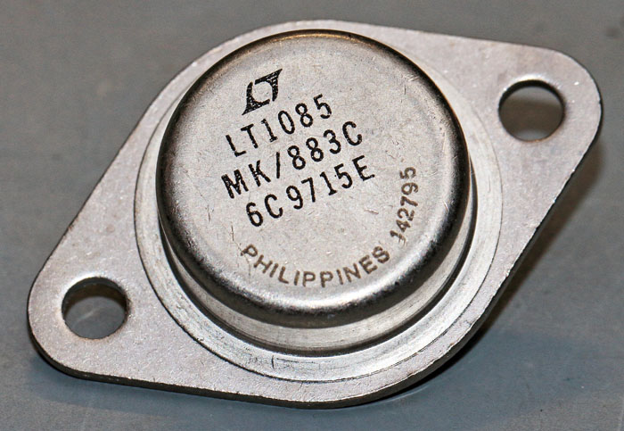
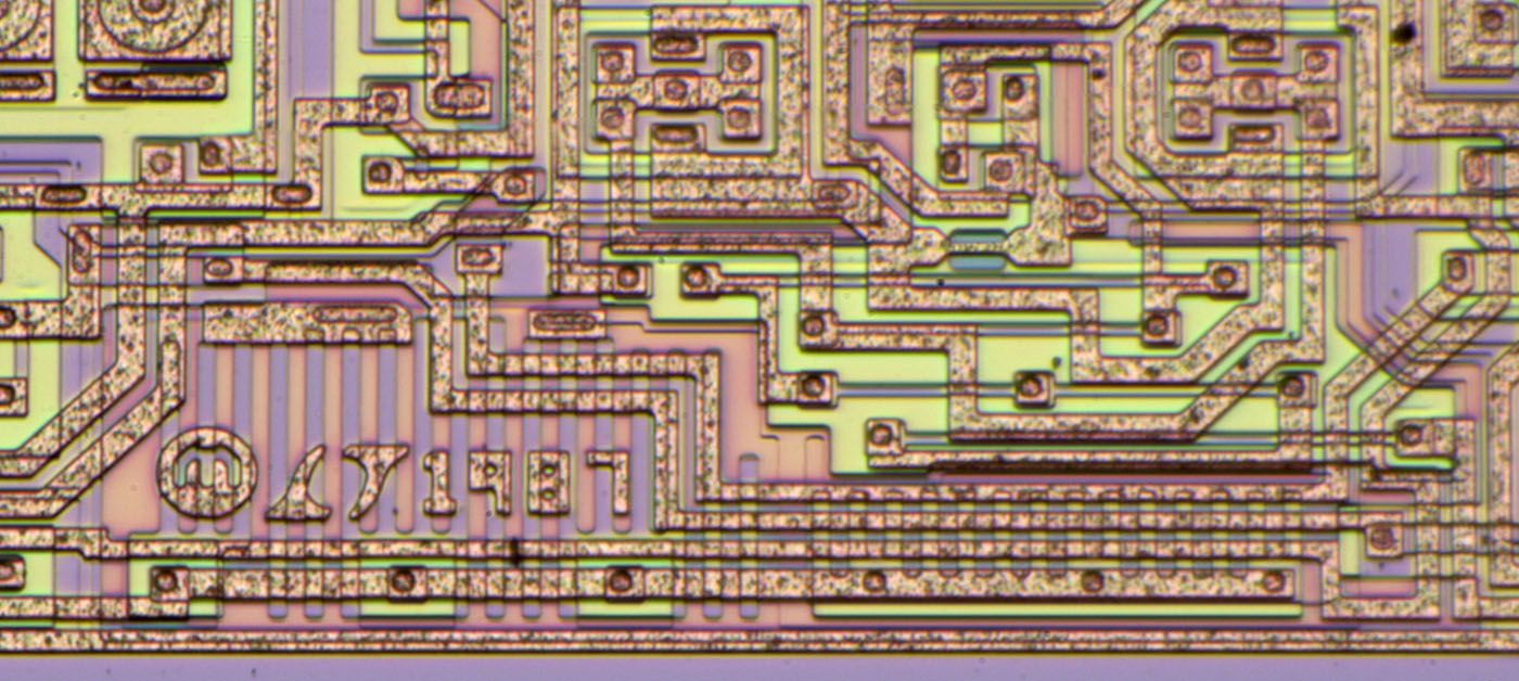
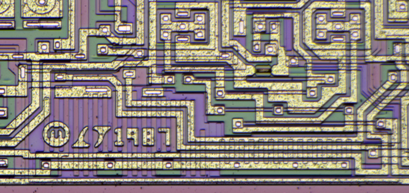
To continue the series today I have the LT1085 for you:


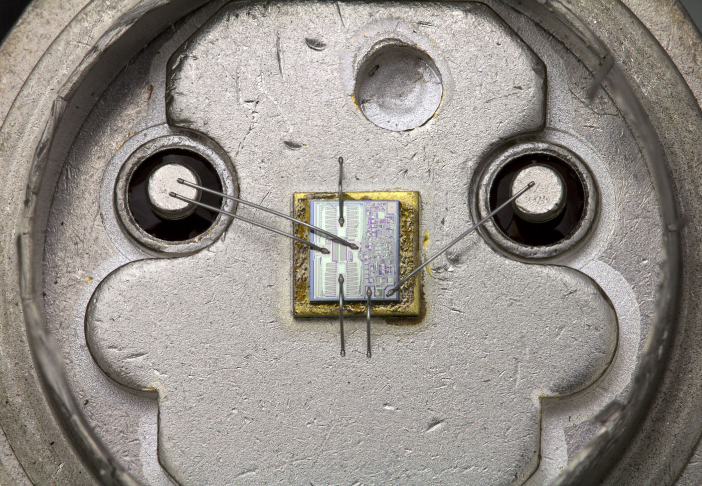
Same big heatspreader but smaller die.


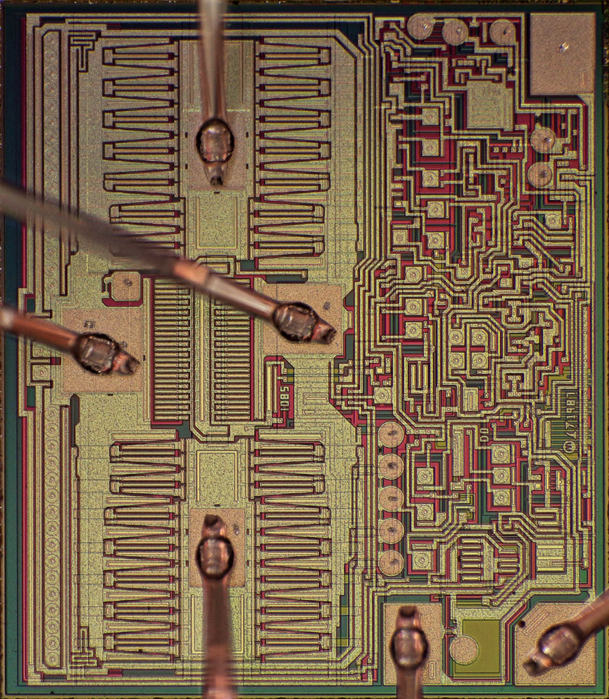
Here you can see they shortened the output stage transistors and cutted the driver transistor in half.
Also reverse protection diode area is smaller.


Another interesting point is the shunt for current limitation:
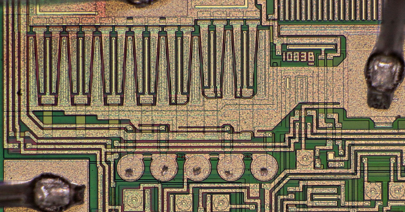


LT1083
A pointy metal line and every fuse is intact.
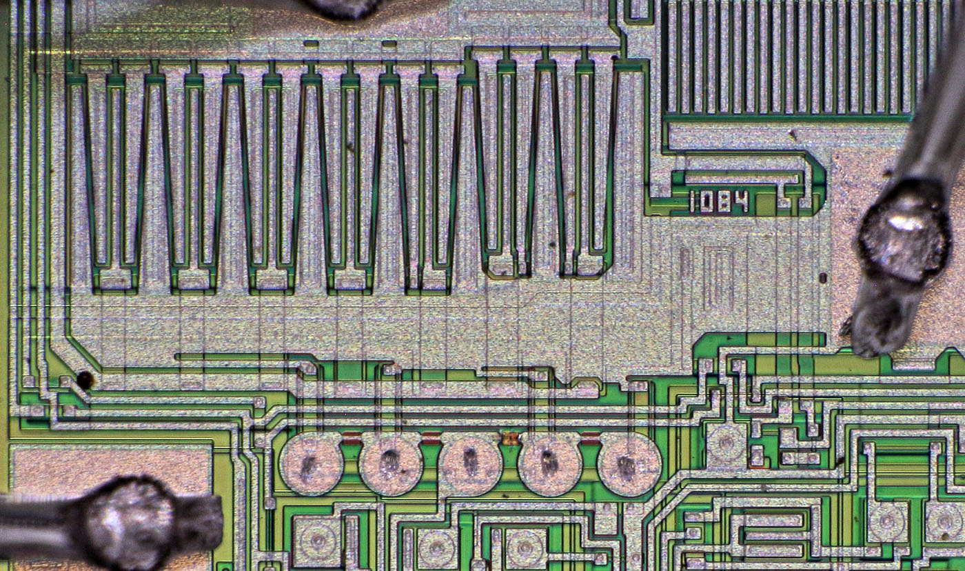


LT1084 (LT1083-die)
A pointy metal line and some blown fuses.
=> Less current to adjust the LT1083-die to a LT1084.


LT1084 (LT1084-die)
A broad metal line and one blown fuse.
=> More current but multiplicated only by two power stages (not four as in the LT1083).
=> The blown fuse shows that the fuses are not only for changing LT108x-variants, they are also used for fine adjustment. Otherwise they wouldn´t have blown a fuse on a LT1084-die to use it in a LT1084.
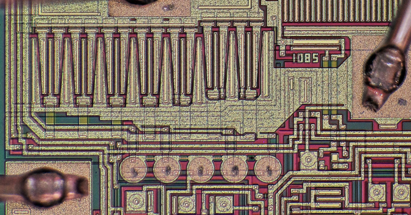
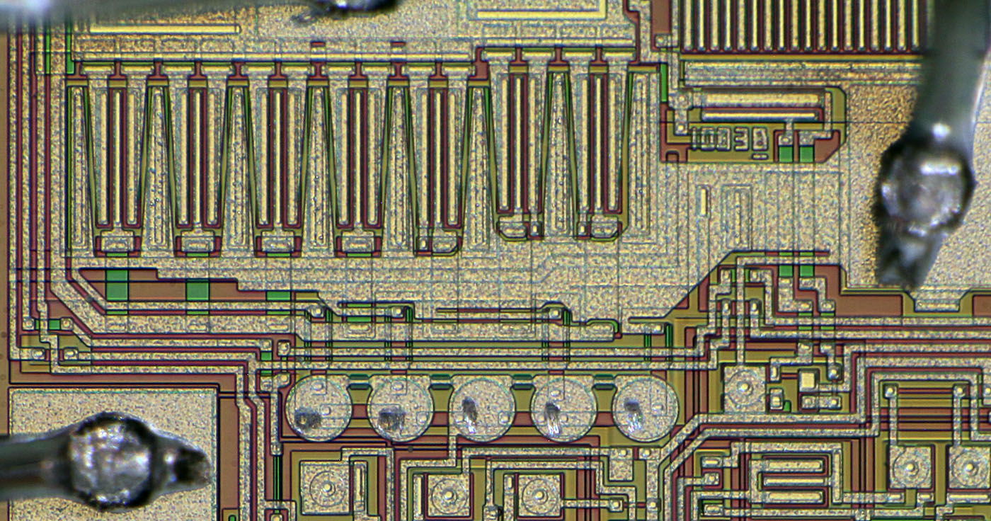


LT1085 (LT1085-die)
A pointy metal line and one blown fuse.
=> Less current.


Anyone an idea what these structures do:


LT1083-die


LT1084-die


LT1085-die

My first assumption was that they use these structures to generate fixed output voltage regulators. The structures are connected to the ADJ-Pin.
Another explanation: That is some change in the control loop. That would explain why it is different in the smaller LT1084- and LT1085-die.

 :popcorn:
 
The following users thanked this post: BravoV, Ice-Tea, RoGeorge


Share me

Digg  Facebook  SlashDot  Delicious  Technorati  Twitter  Google  Yahoo
Smf