Right
I have had a look in detail at the timing and I now agree that C has some valid points regarding interfacing with an 8MHz Z80. Some of these issues also affect the 4MHz Z80 somewhat so in practice might not be show stoppers given that I had a working sound card despite technically violating the timing constraints.
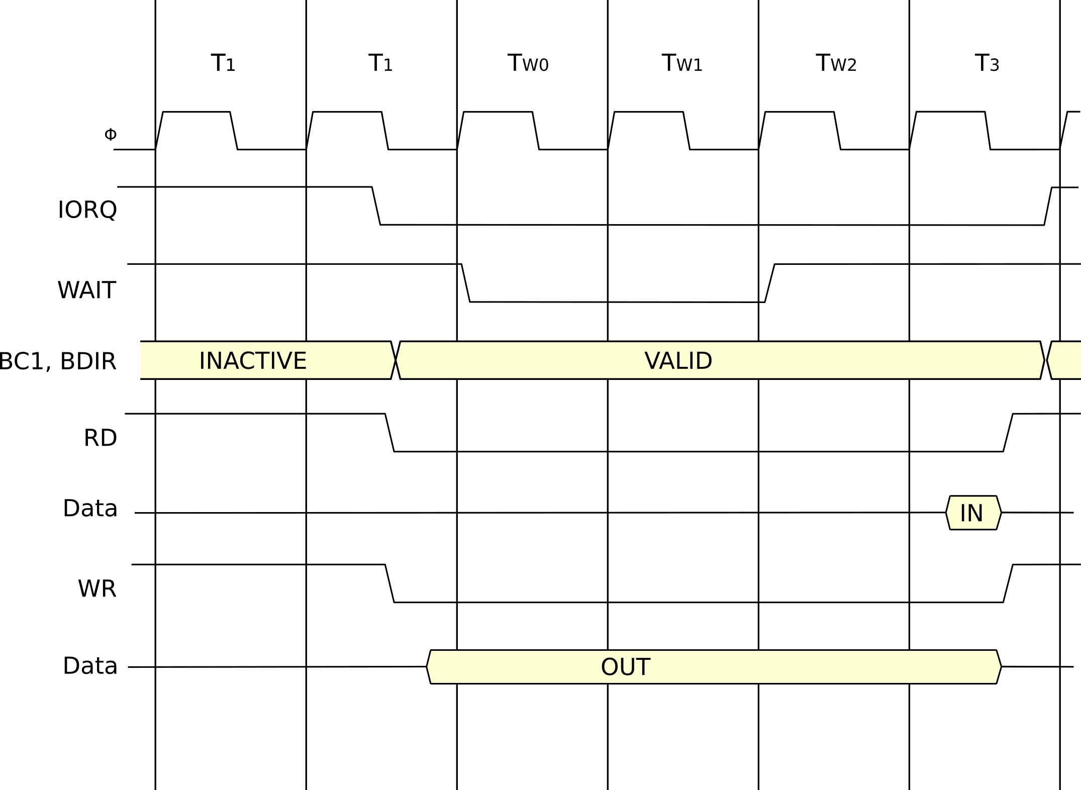
Now we are definitely going to need wait states at 8MHz so I am discussing the timing with that in mind - the I/O cycle timing (loosely to scale with typical propagation delays) looks like this.
Compare this with the AY-3-8912 timing diagrams, first of all the latch address timing.
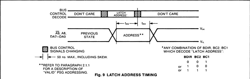
The address is obviously latched as BC1 and BDIR switch back to the inactive state, there are just two timing values
T
AS - the address set up time before the data is latched and
T
AH - the hold time for which the DA
0-DA
7 must remain valid.
T
AS is easily met, the AY-3-8912 spec is 400ns and we have 4\$\small\frac{1}{2}\$ clocks or 560ns at 8MHz so that is fine.
T
AH however,
is a bit of a problem because the 8MHz Z80 only guarantees 15ns of data hold time and the AY-3-8912 wants 100ns
Let's look at the write data timing
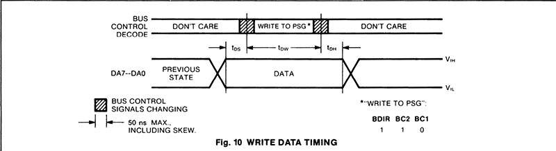
Here we have T
DS - data setup, T
DW - the write pulse width and T
DH, the data hold time.
The write pulse width is OK, we have 560ns and need a minimum of 500ns - that box is ticked.
Then it starts to fall apart. The data setup time is 100ns and, well, the Z80 does not, in fact guarantee that the data is valid when \$\small\overline{WR}\$ goes low. The data hold time has the same problem as the address hold time.
Finally read timing
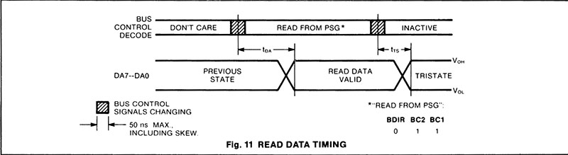
The access time is actually just about OK - the maximum is 500ns and we do just have 500ns to the point where we need the data to be valid, typical is 250ns though which is plenty fast enough.
The tristate delay does mean we could be pushing data onto the Z80 bus well into T1 of the next cycle at 8MHz.
So we have three problem areas, the data hold time on a latch address or data write cycle, the data setup time on a write and the tristate delay - so that's the three places that C identified plus the data setup time issue.
Do these matter?
Well, we would design to these times if we want a robust system but I have the following thoughts.
First off I don't think the tristate delay is significant, at least not for the typical value of 100ns - the cycle following the I/O read will be an opcode fetch - the only way it can be anything else is if you are executing an INI or INIR in which case it will be a memory write (you could take an interrupt, of course) - but nothing very interesting happens on the bus in T1 so the sound chip not having got around to turning its output buffer off is not that big a deal. At 4MHz or slower it definitely isn't going to be an issue, at 8Mhz it should still be OK but I don't think I would push it any further.
Then there is the data hold time. Well, that could be an issue but I "got away" with it with a 4MHz CPU where the Z80 guarantees 60ns of data hold time. In fact if I have calculated it correctly the 8MHz part is better when run at 4MHz as it then has a data hold time of 80ns - and don't forget nockieboy went down to 1.8MHz at which point I think he will actually meet the 100ns.
Finally that data set up time - why is it in the spec in the first place? There isn't an equivalent on the address latch cycle and it's clear the data is latched as BC1/BDIR switch to "inactive" so I find that just odd. It might be worth noting that I "got away" with that one as well.
So I think it is still worth pursuing the current build (I must get back to my own system build as well). At 1.8Mhz I think that all of the PSG timing constraints will be met except the data set up time but I genuinely can't see why the PSG needs that. If it works at 2 or 4MHz and fails at 8 then you know the issue is clock speed.
If it won't work at 8MHz then answer probably
is to use a PIO to talk to it.


