The recent
thread started by
nockieboy reminded me that after the
earlier thread covering Z80 interfacing I had promised myself that I would turn the pile of junk Z80 bits that I have acquired into a "useful" computer.
I have a soft spot for the Z80, what feeble electronics I know stems mainly from fixing early computers in the late 70's and early 80's - mostly Sinclair Spectrum's and also designing and building my own Z80 systems. It all really started with a Nascom-2 I built when I was 16 or 17. I also cut my teeth programming on Z80 systems.
I set myself some totally arbitrary design goals:
- Must support the 20MHz chip (I have one kicking around so why not?)
- Must be buildable on 0.1" perfboard so DIP or PLCC in a socket. SOIC on a carrier only as a last resort
- GALs, PALs and PROMS would be OK but I don't have any way of programming them so in practice glue logic will be plain TTL
- No wait states!
- No using a much more powerful MPU to "nanny" the Z80 along (otherwise I might as well just write a Z80 simulator on a more powerful system)
- Parts must be current, no dipping into the global obsolete parts bin (ebay)
- Banked RAM for CP/M 3 or FUZIX
- CF card for storage
- Video not important, serial console is fine as I probably don't want to play graphical games on it. I can add video later and I might bend the "no more powerful MPU" rule for it, especially if embedded in a COTS display
Sadly one of these wish list items falls pretty much at the first hurdle - no wait states in a 20MHz is probably impossible, at least with banked memory. The problem is that the timing for the 20MHz part sucks a bit.
As usual we start with the M1 cycle which has the tightest timing - here it is with some of the "worst case" timings for the 20MHz part filled in.
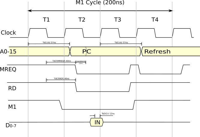
For reference the data sheet with the full timing diagram is
here on Mouser See page 20 for the diagram and 31 for the timings.
The Z80 samples the databus with the rising edge of the clock at the start of T3 and needs 12ns data set-up time. The start of the read cycle would normally be based on the falling edge of MREQ - that is referenced to the falling edge of the clock in T1 but the data sheet says it could be up to 40ns after the clock edge - which is 15ns into T2. Thus we have 50-(15+12) or just 23ns to complete the read cycle.
OK, so fast, half meg RAMs
can be had without difficulty, although I was trying to avoid SMD package adapters (I can't find a 36 pin one anyway). However it's not that easy.
First off I can't find a E/EE/P or FLASH ROM which I can program and which has a 5V supply which also has an access time of less than 45ns. Yes I could get around that by building a ROM-less system and have something else load up the RAM with boot code but I wanted to avoid that.
Second, any gate delays associated with MREQ or the address lines are going to eat into 23ns pretty quickly. In fact it's worse if you look at the official figure for the address set-up time (TdA(MREQf) - address valid to MREQ fall) it is given as -15ns! so the address bus might not even have stabilised by the time MREQ falls - that would reduce the time available for the access cycle to 8ns!
Sadly I decided to just add a wait state to the M1 cycle, that will stretch the needed access time so I can use much more friendly 55ns SRAM and 45ns flash. Just slowing the M1 will have a fairly minimal impact on performance and, to be honest, extracting the last MHz of performance from a Z80 system is a bit like wanting to be the world's tallest dwarf.
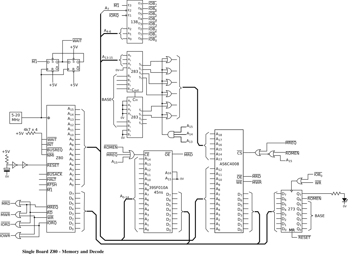
After some thought this is the current state of the design:
I've
previously built systems using two 74F189 TTL RAM chips to make a fairly flexible mapping based on 4k pages which will allow access to 1M of RAM. Sadly the 74F189 is no longer available new.
So I have used a different scheme here. Using two 74283 4-bit full adders to make an 8-but adder the upper part of the address bus is formed by adding a fixed base address (specified by writing the base to a latch) to the top three bits of the address bus. In this way the 64 address range of the Z80 can be used as a window into a larger address space. In this case I am going to make it 512K.
The top 8k page is forced to the top of physical memory to provide a common page - this is exactly how CP/M 3 wants to set up banked memory.
Using a 512K RAM gives 504K or 9 banks of 56K exactly which is a nice fit.
32K of ROM space is provided - this is mapped into the low 32k of memory when the ROMEN signal is active.
On reset the ROM is enabled and the bank base address set to 0, the boot code can then copy code up to the top of RAM and then jump there which can disable the ROM.
Memory timing is still dodgy. If I use 74F283 adders the propagation delay for each is about 5ns, plus 6ns for a 74F32 OR gate making 16ns in total for the address manipulation.
If the address really is not stable by the time MREQ goes active an extra 16ns delay with a 55ns RAM is too tight (58-16 = 42ns, oops). Ideally one would design to worst case not typical (or even best case) timings but I think I should be OK. In fact I will probably be OK with 74ACT parts which are only very slightly slower than 74F so I'm going to go for those first as 74F is a bit power hungry (up to 55mA per chip for the adder).
I still have to do the serial and CF card interface. The "easy" cop out of using the Z80 peripheral chips is actually not available as they do not (as far as I can see) exist in 20MHz speed. Also common UART chips like the 16550 are actually a bit slow on their data access times for a 20MHz Z80, even given that the IORQ cycle is slowed with a CPU generated WAIT state.
More when I have finished the I/O design.


