Hey,
Response:
So I know it looks like I just have my V/div turned down too low, but I am 100% certain that is not the issue (I have just revisited adjusting the knob settings). If necessary, I can upload a video of myself adjusting the scope settings while measuring the cal signal?
Update:
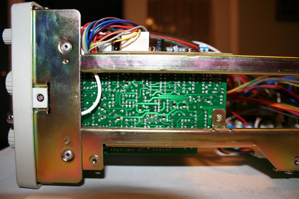
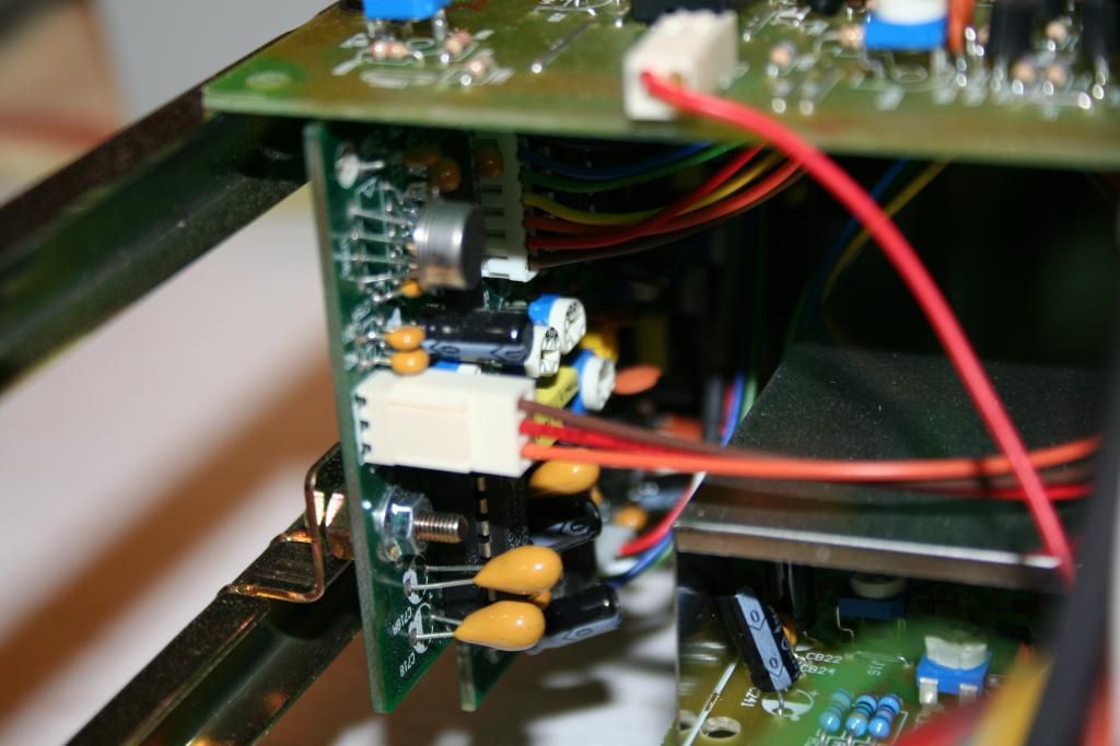
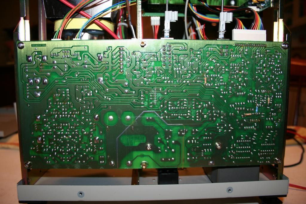
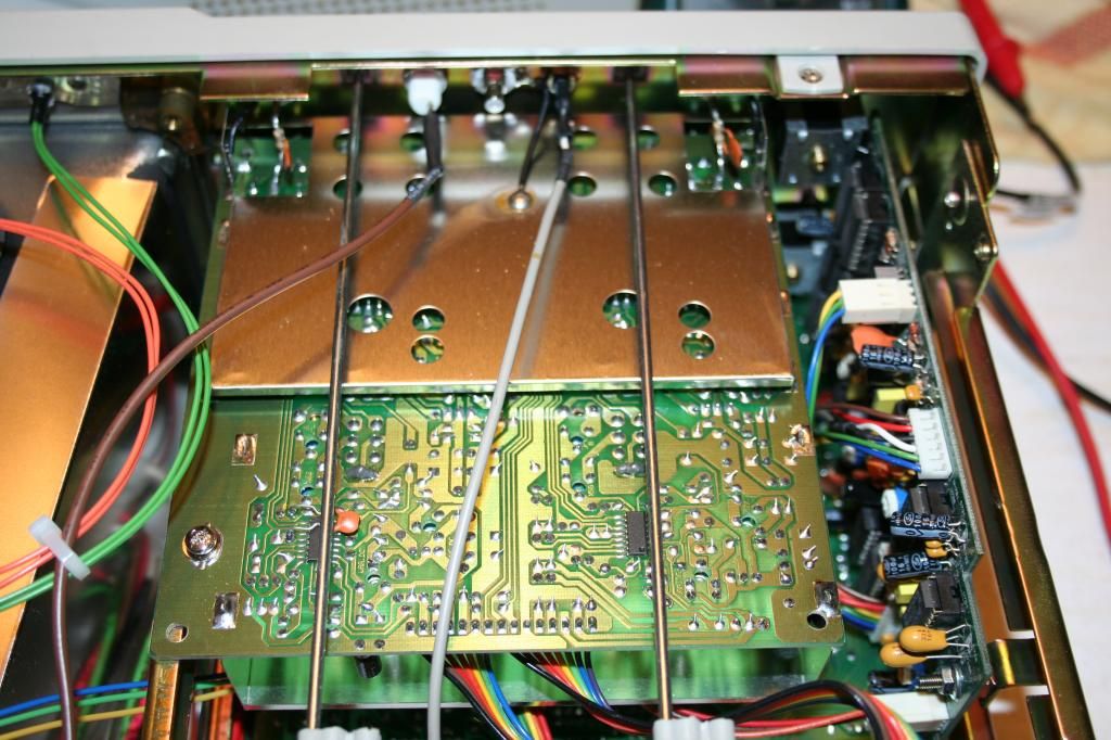
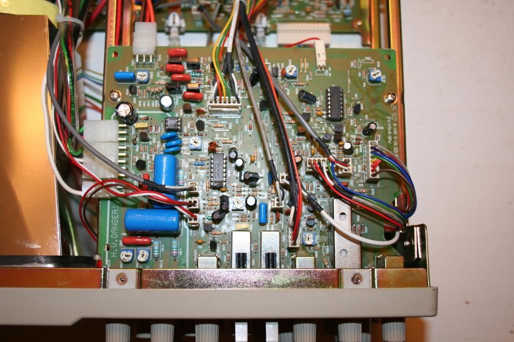
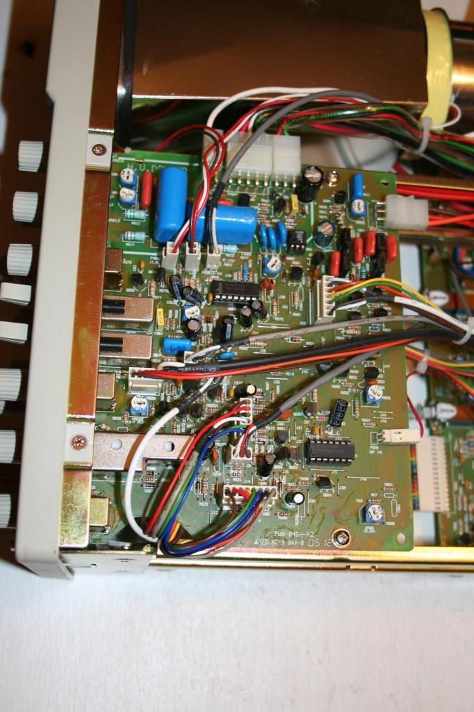
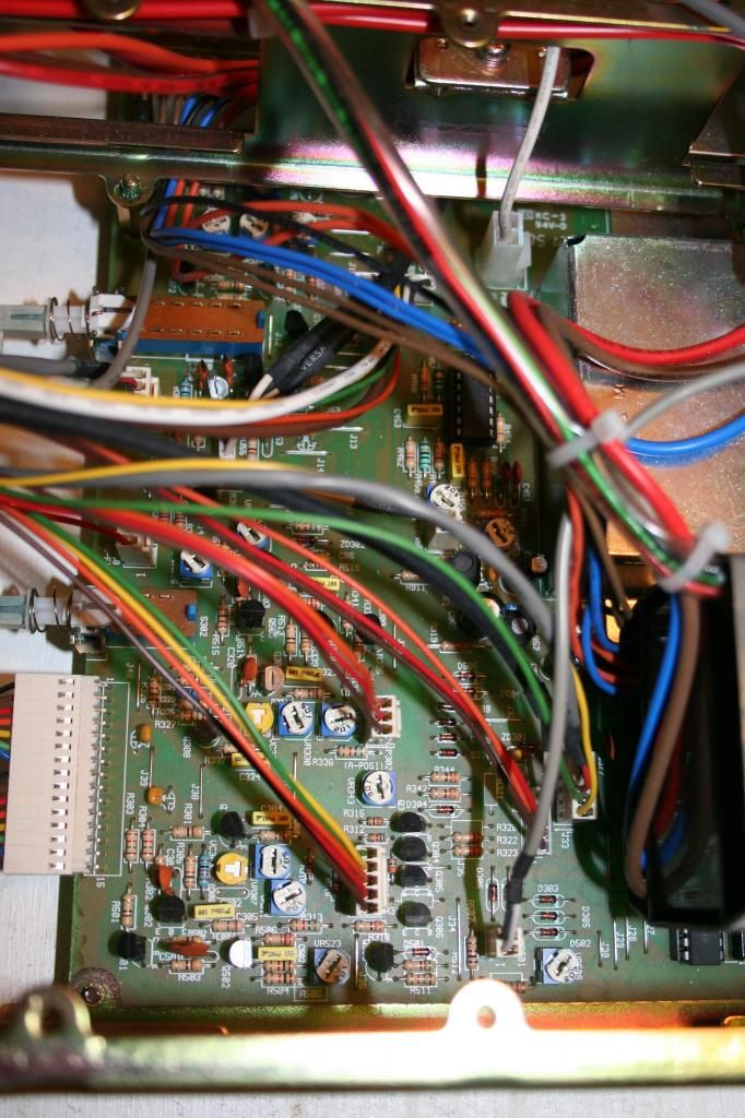
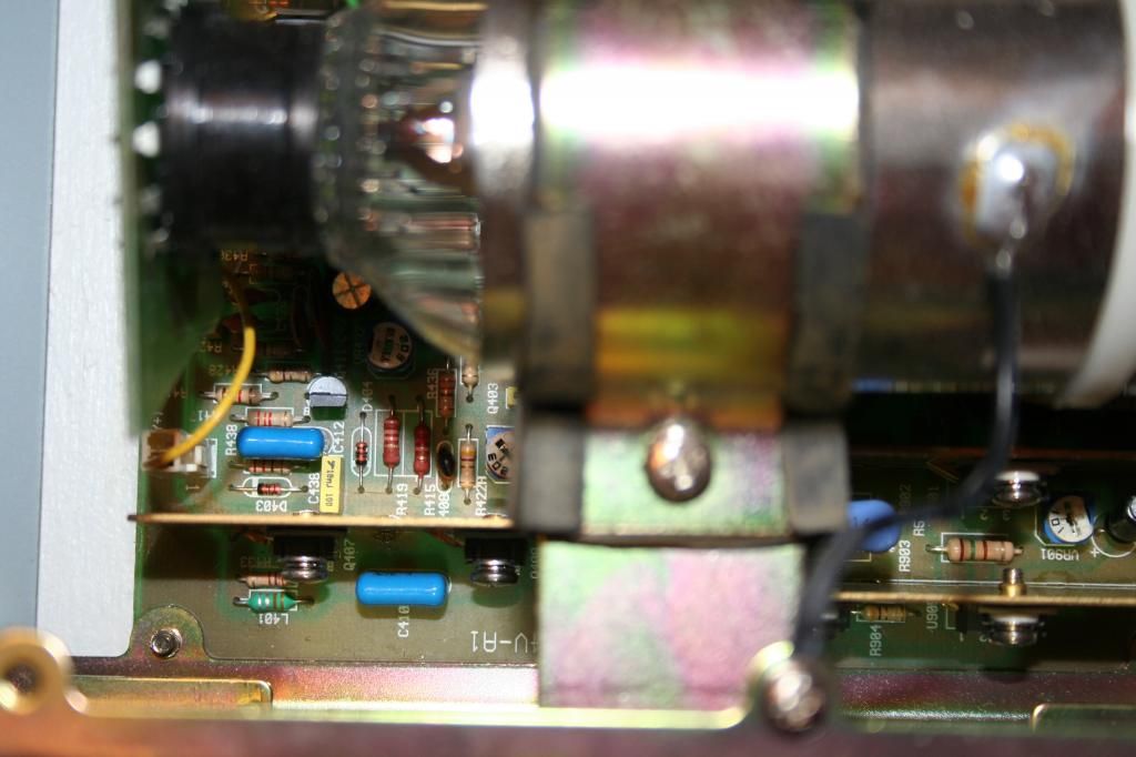
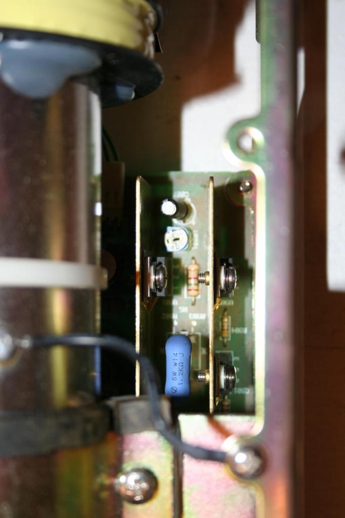
So I have uploaded some close up pictures of the internals. Sorry if they don't show much, it's hard to get good internal shots will all the wires in the way and board mounted awkwardly. I have also uploaded scans of the original schematics for the 2160A model. However, the board layouts seem to be slightly out of sync with my scopes boards. As you can see, the schematics show versions D,F, etc., where my boards seems to be on revision A.
In one picture I have uploaded, you can see that I am testing the cal signal from my Oscope (2Vp-p, 1kHz) with both the Oscope and a USB "Analog Discovery." The Oscope's cal signal seems to be spot on, but I am still getting a bad reading on my Oscope. One thing I noticed is that the trigger level seems to do absolutely nothing to the measured signal on my Oscope, that doesn't seem right!
I probed around some more for all the sub-HV rails, and all the voltage rails seems to be fine. However the two two 16V differential pairs coming off the main transformer were both reading out a stable 20V, is this something to worry about? Every other rail was within +/-1% of the designed value.
Questions:
1) Is there somewhere I can probe around to test for my trigger signal? I have two rear BNCs labeled "Z-axis input" and "CH-B(Y) Signal Output."
2) With all the High Voltage circuitry present, when is all the residual energy dissipated and safe for me to probe around? Some of these boards are buried in the chassis and I would like to remove them for easier examination safely.
3) What else should I be doing to further debug my Oscope? I am feeling kind of lost right now :/
Thanks!

!!!Here are the Schematics to the scope!!!
https://drive.google.com/file/d/0Bzao2JBCAMY0YWYtbFFJLW9xcFk/edit?usp=sharing 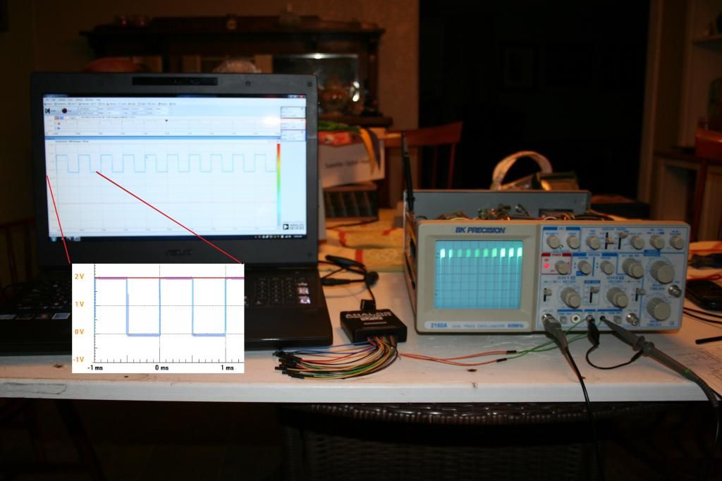
Solder side of PSU board
Solder side of vertical amplification circuit (I believe)
Component side of CRT control, trigger, and possibly position and time pos. circuit
Component side of PSU board:
Component side of PSU board on left side of CRT:
Time/div and Time/delay circuit: