OK, as promised - some photos to complement those from HighVoltage, and the start of repair efforts.
All the images are linked to a full-size version.so just click on the image if you want a more detailed view.
First of all this is what the inside
should look like when it hasn't been mangled by poor packaging and being used as a football by the courier. This is my 3382 rather than the 3394 but they are essentially identical.
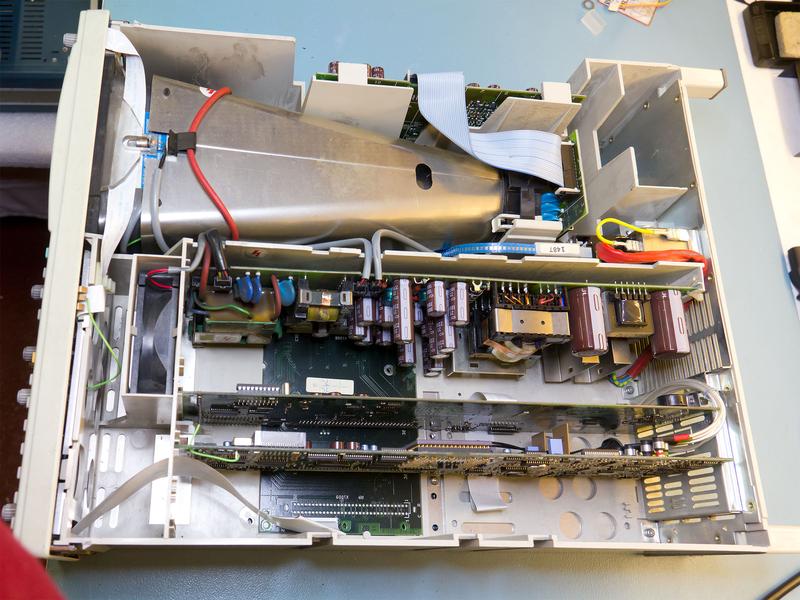
The lowest card in the picture above is the acquisition and data processing card A8 - basically the DSO part of the 'scope plus triggering and text generation. It has several custom chips, two 200Ms/s ADC's and a TMS 320C25 DSP. I'll probably need to have a more detailed look at this card to figure out why I'm not getting any readout text from the 3394.
The next card up is the main CPU A3, then the power supply A6 and at the top, just visible the final X, Y and Z amp board A2.
Underneath is the A1 board carrying the analogue front end and signal paths.
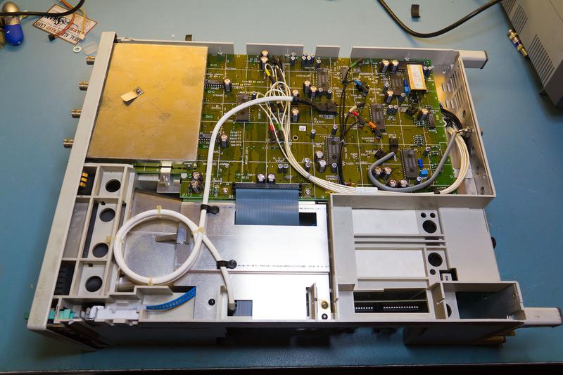
The white coax carries differential signals from each of the four channels to the digital board. If you look at the first photo you can see how these loop up and over the RS232 connector on the CPU card, making it almost impossible to remove, in the end I just unplugged them - I don't need the digital section to work to debug the CPU to UFO link. They are neatly colour coded though - if you look carefully at the full sized version you can see that each of the connectors on the board has a coloured ring which matches the one on the cable.
The black coax brings some signals back - mostly related to TV triggering. Just about every chip on the A1 board apart from the TEA1017 serial to parallel converter is a custom Phillips part so if these die the only option is a swap from another 'scope. Even the TEA1017 is obsolete so not all that easy to come by.
The front panel connector is in a spectacularly awkward place. I've ended up cursing this several times. Worryingly there appears to be provision for a further card in the chassis - I don't know what variant of the 'scope would have that but it would be impossible (rather than merely very difficult) to connect and disconnect the front panel ribbon cable with it in place.
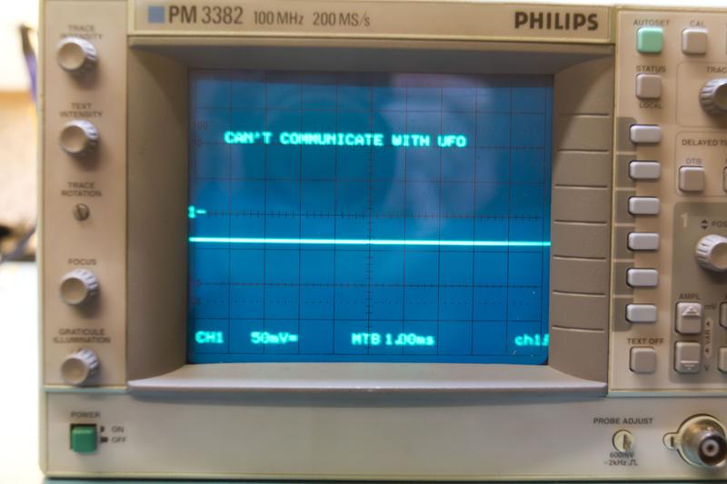
So if you remember the problem was that ET couldn't phone home.
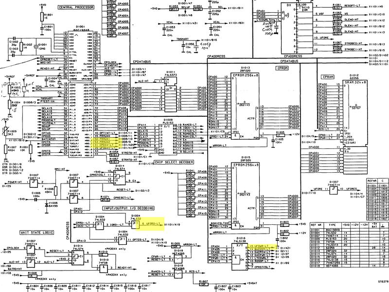
A total of 4 signals provide the handshake between the main CPU and the front panel processor. Looking at the circuit diagram for the CPU card 2 of these signals are generated from address decode logic and two connect directly to the CPU. This is difficult to see on the reduced size version so do look at the original if you want to see what's going on..
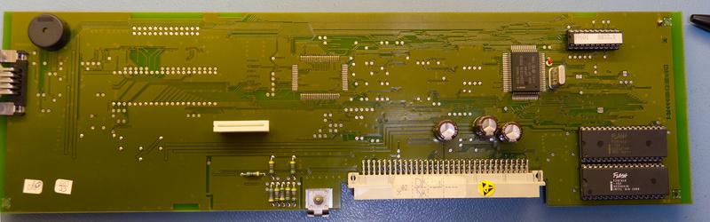
CPU card processor side - there's really very little going on on this card. The main processor is an 80C196 in qfp package which you can see just above/to the right of the three capacitors. There's a GAL used for decode (DIL chip with label) and two flash ROMS. To the left of the board there is the (unpopulated) GPIB option.
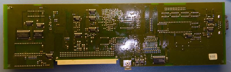
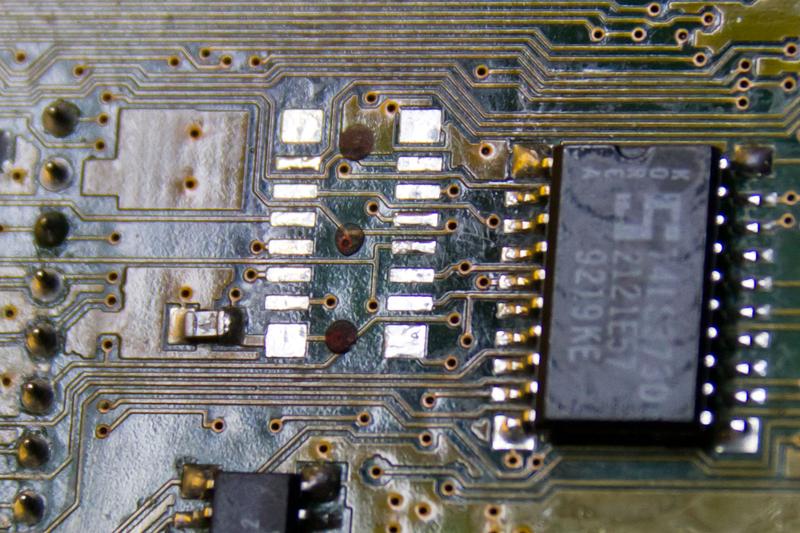
The rear of the CPU card is slightly busier. Over on the left the largest chip is a 32kx8 SRAM ffor the main CPU, various discreet logic in the middle and more unpopulated areas for the GPIB option. We're interested in the 74LS32 and 74LS138 just above/to the right of the SRAM.
Actually debugging the signals is not all that feasible. For one thing the getting a probe to the rear of the card would be impossible. For another we're probably trying to capture just one event as the CPU card resets the front processor and tries to establish comms with it so the easiest way of debugging the fault is just to swap suspect parts and see what happens. I'll do the 74LS138 first as a) I happen to have a replacement handy and b) when I first got the CPU card out it was obvious that the 74LS32 has already been replaced.
So, out with the hot air gun on the rework station and here are the pads cleaned and tidied for the replacement.
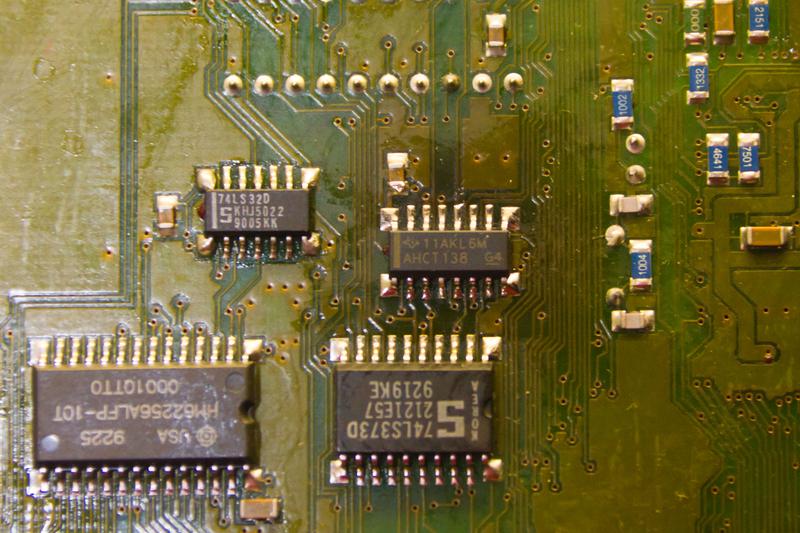
The spare turned out to be an 74AHCT138. I really can't remember why I bought these. Still it's just as well that I did

Looks like I cooked the conformal a bit too much - oh well, I'm still getting used to working and re-working SMD parts. At least I didn't lift any pads this time unlike my FE5680A

Turn the 'scope back on and -
TA-DA
So, there you are - we're up an running on the CPU board at least. I hope you all enjoyed the photos and going through a bit of logical hardware debugging (plus a smidgen of luck).
Hopefully I can get the text readout sorted as well. However I think the first thing is to swap the CPU cards back into their respective 'scopes and probably close up the 3382 and put it back on the bench as a 'scope, not a test-bed. I doubt swapping the 3394 A8 card into the 3382 will give me any useful information and swapping my 3382 A8 card into the 3394 won't quite work correctly anyway as the 100MHz and 200MHz A8 cards are slightly different (and will probably be detected as a wrong hardware version by the CPU).
Watch this space.


