I cannot read that code very well. I have a simple Arduino register loading sketch.
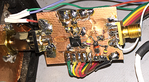
John: please refer to the picture attached. Do you expect any problems from this setup?
Looks like the connections are OK, although the grounding is questionable in my experience with these chips. (Haven't used the ADF4001 myself but I've used plenty of ADF4002s.) I'd recommend mounting the chip directly to copper, either live-bug or dead-bug style. Even then, you want to keep the VCO and reference paths away from each other.
For example, here's an ADF4002 with a small 38.4 MHz VCXO just to the right of it (click for much larger version):
Also, you might try a wider loop BW to begin with, say 1000 Hz. Is R1 in series with the charge pump output? If R1 is 60K and Vp is +5, your charge pump current can't exceed about 80 microamps, regardless of the Rset resistor or Icp register values. So the loop may be OK in theory but not in practice. Post your ADISimPLL file if you like.
Edit: Another pitfall that's not in the book is that those ceramic SMT capacitors like the 0603 (or 0402?) part you have between pins 4 and 5 are hard to hand-solder reliably. The end terminations like to detach without leaving any visual evidence. If the cap survives soldering, it may also open up due to differential thermal expansion during normal operation if a small length of wire isn't used as a strain relief. Not too likely here, but if (e.g.) one end of the cap were soldered to a ground plane and the other connected directly to an IC pin, thermal stress would be a concern.
So you might unsolder the capacitor to make sure it's actually OK. Afterward, use a new capacitor, rather than reinstalling the old one.


