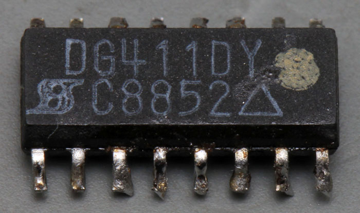
Author Topic: Replacement for Fluke 700013 IC (quad SPST analog switch)  (Read 13471 times)

0 Members and 1 Guest are viewing this topic.

Offline Kleinstein

  • Super Contributor
  • ***
  • Posts: 14206
  • Country: de
Re: Replacement for Fluke 700013 IC (quad SPST analog switch)
« Reply #75 on: February 20, 2022, 07:46:16 am »
I´m not sure why they have integrated the capacitors.  :-// I assume they stabilize the gate potential against the input signal.
Chances are the capacitors are there to reduce the charge in jection / switching spike. The P-MOS transistor is quite a bit larger than the NMOS and thus more gate charge there.
 
The following users thanked this post: Noopy

Offline Noopy

  • Super Contributor
  • ***
  • Posts: 1734
  • Country: de
    • Richis-Lab
Re: Replacement for Fluke 700013 IC (quad SPST analog switch)
« Reply #76 on: February 20, 2022, 08:32:37 am »
I´m not sure why they have integrated the capacitors.  :-// I assume they stabilize the gate potential against the input signal.
Chances are the capacitors are there to reduce the charge in jection / switching spike. The P-MOS transistor is quite a bit larger than the NMOS and thus more gate charge there.

That perfectly makes sense!  :-+

Offline Noopy

  • Super Contributor
  • ***
  • Posts: 1734
  • Country: de
    • Richis-Lab
Re: Replacement for Fluke 700013 IC (quad SPST analog switch)
« Reply #77 on: October 29, 2022, 08:13:17 pm »


TiN had sent me a Siliconix DG408. It is an 8-channel analog multiplexer. Like the DG411, the DG408 can be supplied with up to 44V and then allows switching of potentials up to 40V. The typical Rdson is minimally higher at 40Ω. The switching times are just above 100ns and thus correspond to the switching times of the DG411.


The datasheet of the DG408 contains a circuit diagram that shows how the device works. Three inputs allow the selection of one switch. In addition there is an enable interface. All inputs have protection diodes and are supplied by an internal voltage regulator. A level shifter adjusts the level of the control signals before they pass through a decoder circuit that controls the eight switches. An interesting fact is the simpler construction of the actual analog switch compared to the DG411. In the DG411, the bulk potential of the NMOS transistor is varied during switching, whereas in the DG408 it is just tied to V-. Protection diodes are integrated in the analog switch area too.


At first glance, the specifications of the DG408 and the DG411 look very similar. However, the diagrams in the datasheets show that the Rdson varies more with the DG408 than with the DG411. These characteristic curves look similar at first glance too, but you have to consider the different step sizes of the vertical axes.


The dimensions of the die are 2,4mm x 1,7mm. The distribution of the function blocks is easy to see. In the right area, there are two big transistors arranged around each of eight bondpads. The bondpad that contacts all analog switches is on the right edge. In the left area and between the analog switches the control circuit is integrated. The capacitor in the upper left corner probably belongs to the internal voltage regulator.


The DG408 was designed 1994 by Siliconix. While the DG411 had the characters CSHN, the letters CSICI are found here. Perhaps these are the initials of the developers. Perhaps there is a manufacturing process behind the abbreviation. The C in the second line seems to have its own meaning. It could be that the revision is depicted here.


Exposing the die has damaged the metal layer somewhat. Some smaller areas have dissolved.

On the analog switches, it is noticeable that the PMOS and NMOS transistors have a very different contacting. One transistor is connected with diagonal leads. These are usually square drain and source regions that alternate within a line and are offset from line to line. The other transistor has horizontal and vertical contact strips, respectively. Here, the drain and source seem to be designed as larger strips. Probably the shapes optimize the electrical properties so that the resistance is as constant as possible.


https://www.richis-lab.de/aswitch07.htm

 :-/O
 
The following users thanked this post: TiN

Offline Noopy

  • Super Contributor
  • ***
  • Posts: 1734
  • Country: de
    • Richis-Lab
Re: Replacement for Fluke 700013 IC (quad SPST analog switch)
« Reply #78 on: December 26, 2022, 04:49:29 am »


Siliconix DG411...

[...]

https://www.richis-lab.de/aswitch06.htm


We had the DG411 now let´s compare it with the DG444. The Siliconix DG444 is a 4-channel analog switch like the DG411. The two devices have many things in common. However, when an analog switch is closed, the DG411 offers a lower resistance of 35Ω maximum. In the case of the DG444, one must expect up to 85Ω. In return, the parasitic capacitances of the DG444 are lower. The typical charge displacement of 1pC is just one fifth as large as with the DG411. In addition to the DG444 with NO switches, the DG445 offers the same switches as NC types.


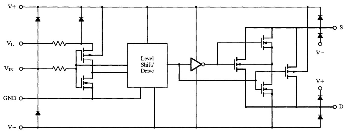
The circuit diagram shown in the datasheet contains the same parts as in the datasheet for the DG411.


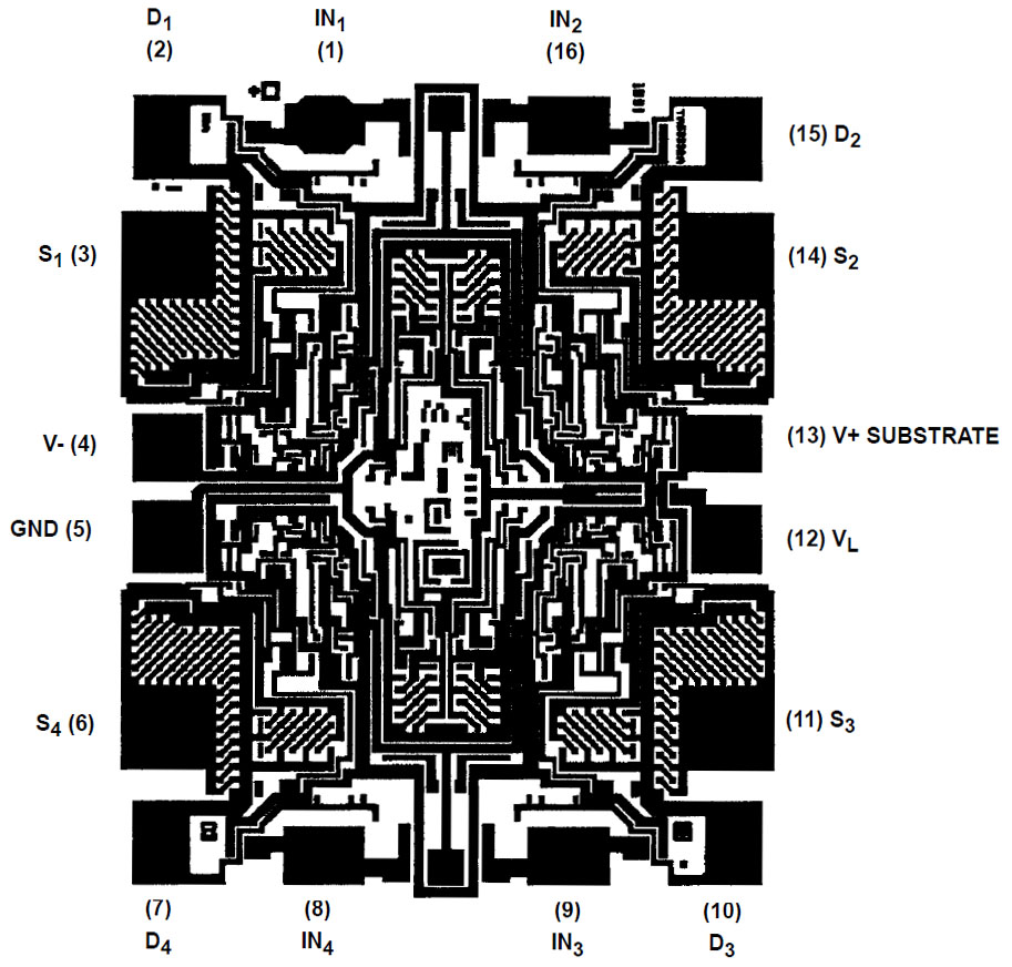
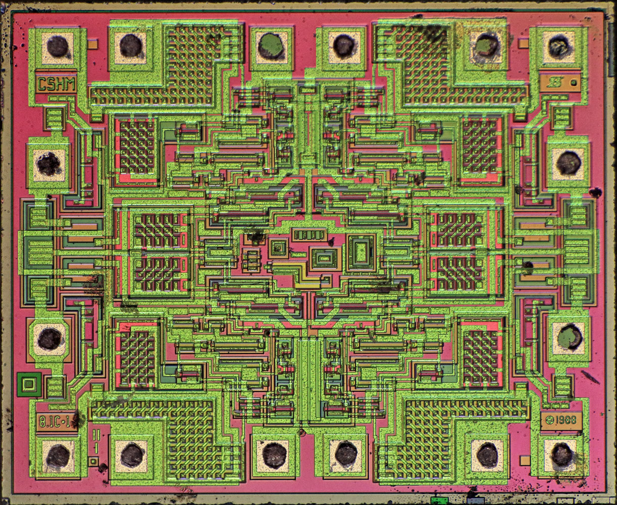
The datasheet includes an image of the metal layer and specifies the size of the die as 2,16mm x 1,76mm. It is thus noticeably smaller than the die of the DG411.


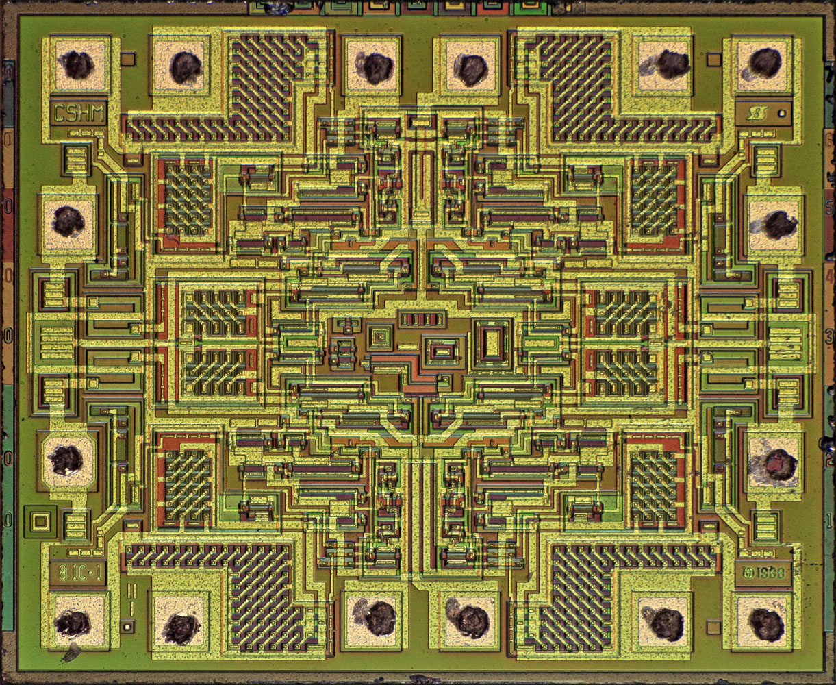
The metal layer on the die largely corresponds to the representation in the datasheet. Apparently, just the additional markings and labels have changed somewhat.


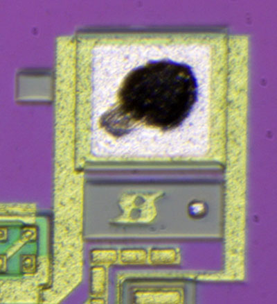
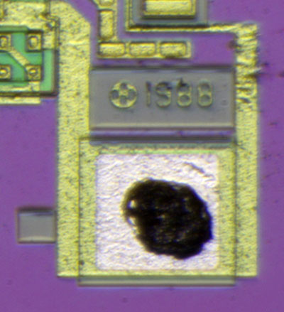
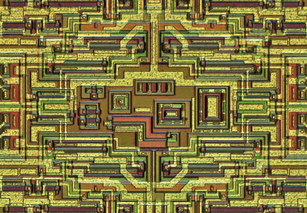
Different inscriptions are shown in each corner of the die, including the Siliconix logo and the year 1988.


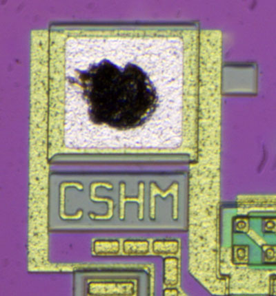
The string CSHM is probably the internal designation for this type of analog switch. On the DG408 the characters CSICI are shown, on the DG411 it is the characters CSHN.


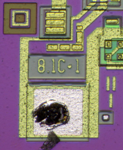
As on the DG411, there is also a character string that presumably identifies the variant of the metal layer and thus the analog switch. It seems very likely that on the same die, besides the DG444, the DG445 can also be realized.


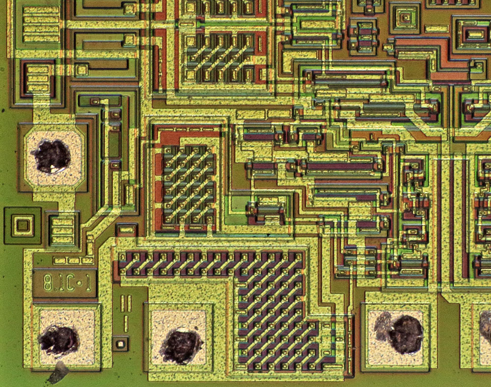
Some areas, such as the structures at the inputs, are built in the same way as the DG411. The large switching transistors have the same structures, but are much smaller. This was to be expected due to the specifications. Interesting is the capacitor on the right of the left bondpad. This capacitor makes it possible to keep the charge injection low during switching. The capacitor offers several surfaces that can be connected as required to optimize this effect.


In the center there are some unused elements. Maybe the inversion of the control logic is realized here (DG444/DG445).


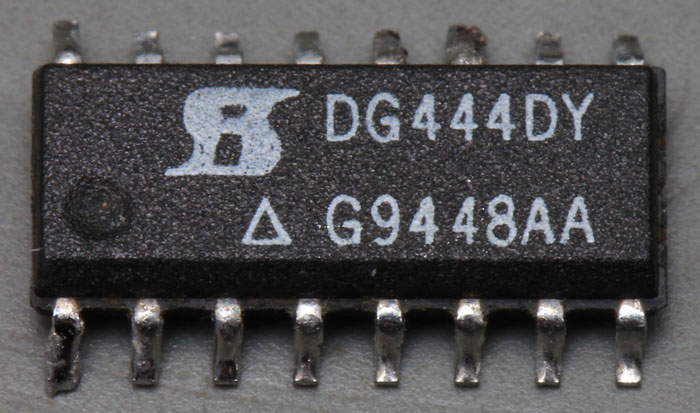
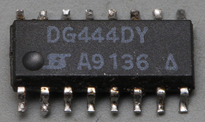
The printing on this DG444 looks significantly different from the DG444 above. The second line seems to be a date code. This would make the analog switch shown here 3 years younger.


It turns out that it is the same die.


https://www.richis-lab.de/aswitch08.htm

 :-/O
 
The following users thanked this post: SeanB


Share me

Digg  Facebook  SlashDot  Delicious  Technorati  Twitter  Google  Yahoo
Smf