Author Topic: Replacement for Fluke 700013 IC (quad SPST analog switch)  (Read 13456 times)

0 Members and 1 Guest are viewing this topic.

Offline JoergR

  • Contributor
  • Posts: 21
  • Country: de
Re: Replacement for Fluke 700013 IC (quad SPST analog switch)
« Reply #50 on: June 11, 2021, 07:51:12 am »
Just got recommended this on eBay - seems like someone is already going to production with this ;-)
It uses a DG212 and an unidentified second chip - likely a uC?
 

Online Kleinstein

  • Super Contributor
  • ***
  • Posts: 14197
  • Country: de
Re: Replacement for Fluke 700013 IC (quad SPST analog switch)
« Reply #51 on: June 11, 2021, 07:57:25 am »
The task for the logic is not really suited for a µC (needs to react quite fast, e.g. some 300-1000 ns for the latch pulse). Possible, but I would more expect some PLD / CPLD - though here the 5 V compatibility could be tricky.
 

Offline JoergR

  • Contributor
  • Posts: 21
  • Country: de
Re: Replacement for Fluke 700013 IC (quad SPST analog switch)
« Reply #52 on: June 11, 2021, 08:38:59 am »
Something like an ATF16V8, maybe? Those are 5V.
 

Online Kleinstein

  • Super Contributor
  • ***
  • Posts: 14197
  • Country: de
Re: Replacement for Fluke 700013 IC (quad SPST analog switch)
« Reply #53 on: June 11, 2021, 09:07:25 am »
The PLD looks plausible and should work.
 

Offline Dakkahun

  • Contributor
  • Posts: 25
  • Country: ro
 
The following users thanked this post: edavid

Offline JoergR

  • Contributor
  • Posts: 21
  • Country: de
Re: Replacement for Fluke 700013 IC (quad SPST analog switch)
« Reply #55 on: June 29, 2021, 09:42:48 pm »
So the boards on my vertical layout that I had posted previously came and lo and behold - the worked perfectly - except that I mixuped up the order of the output switches  :palm: .... So I've removed that post from the thread and fortunately only one person had downloaded it... Sorry for that  :-[. Back to the drawing board and inspired by the horizontal setup posted above, I made another layout with correct switches this time. The boards came a couple of days ago. I've put sockets on the main PCB this way the daughterboards are raised high enough to be clear of all other parts. With U301-303 replaced all self tests passed!  :phew: DC voltage and current appear to work fine. Only in the low AC current range around 1mA there is a larger error - but I guess that can be fixed with calibration as I had previously erased all calibration values. I've used the DG411 and the 74AC logic chips. Only the Ohms circuit still gives me trouble. It only measures correctly on the 20k range and outputs the correct current of 1mA. So I suppose I also have to replace the remaining two 700013 ... I need to order the DG211 first, though.

If someone is still in need of replacements - I have a few PCBs to spare.

Thanks a lot again for the help I got here!
« Last Edit: June 29, 2021, 09:46:37 pm by JoergR »
 
The following users thanked this post: edavid, coromonadalix, ch_scr, jemotrain

Offline richipediaTopic starter

  • Contributor
  • Posts: 20
  • Country: de
Re: Replacement for Fluke 700013 IC (quad SPST analog switch)
« Reply #56 on: June 30, 2021, 02:38:58 pm »
That mechanical design looks very nice. Good combination of THT and SMD parts to use space efficiently!
 
The following users thanked this post: JoergR

Offline JoergR

  • Contributor
  • Posts: 21
  • Country: de
Re: Replacement for Fluke 700013 IC (quad SPST analog switch)
« Reply #57 on: July 01, 2021, 08:15:14 pm »
In hindsight, and looking at the pictures now, I feel that the switch chip should be moved over a bit to the edge of the board. The header pins don't need to be below the center of the chip. That would give the capacitors a bit more space. Oh well, ... I'm attaching the KiCad Files if someone still needs those.
I got the DG212 chips today and combined them with 74AC08 AND gates and now the meter is all up and running again.  :-DMM
That's the nice thing about richipedia's design, one can choose different chip combinations DGX12 + 08 AND or DGX11 + 00 NAND on the same board.
 

Offline Kjo

  • Regular Contributor
  • *
  • Posts: 81
  • Country: us
    • Hollywood Controls
Re: Replacement for Fluke 700013 IC (quad SPST analog switch)
« Reply #58 on: July 03, 2021, 10:49:52 pm »
I spent a good deal of time during COVID working on the same concept and reported progress at the Fluke list over at groups.io.
I started by trying to use a PIC16F15323 to control a DG212B. It has 4 CLBs that can implement registered logic independent of the
instruction counter. Fluke timing for the 700013 is not that critical, but it wouldnt work in all 700013 positions. |O
I also tried 2 versions using 4000 series and 74HC series. Still had some issues. >:D Finally I landed on a 2-chip solution with a PLD & DG212B.
That version worked flawlessly and is only 40% bigger than the 700013 IC itself. :-+ Assembly is all SMD in SOIC packages & 4 0603 capacitors.
I put together a kit for the MK5 version for $18.95.
https://www.hollywoodcontrols.com/phpFluke/HC700013P.php

I also have a Z8611 clone I am looking at kiting. Similar to others out there. Based on U8840M.

You can also find pretty much all the ROMs that are in the wild there too.

kjo - KO3Y

 
The following users thanked this post: edavid, coromonadalix, wolfy007

Offline Noopy

  • Super Contributor
  • ***
  • Posts: 1734
  • Country: de
    • Richis-Lab
Re: Replacement for Fluke 700013 IC (quad SPST analog switch)
« Reply #59 on: July 07, 2021, 03:53:41 am »


TiN had sent me an ADG444B. I have thought about posting it in my "normal" Die-Thread but since you are talking a lot about analog switches (DG211) I will post the ADG444 here.


The die is 1,9mm x 1,7mm. You can easily spot the four switches.


The datasheet describes a ADG444A which is fabricated with an buried oxide layer to isolate the integrated transistors. The isolation prevents latch-up but probably also reduces leakage and crosstalk.


The die doesn´t look like to have this isolation layer.
In the OPA627 (https://www.richis-lab.de/Opamp22.htm) we have seen that it is possible to see an isolation layer at the side of a die.
But this is the B-version of the ADG444. No isolation to be expected.


A 1993 design.


Internal naming?


We see six mask revisions.
Nice big transistors.


Etch marker or mask alignment help.


Now that is a nice pin 1 marker!  8)


Here we see one switch built with two big transistors (PMOS and NMOS).


That is interesting:
The bulk of the upper transistor T1 is connected to Vdd. That is probably the PMOS. It´s switched with Ga.
The lower transistor T2 has to be the NMOS. It´s switched with Gb. It´s bulk is connected to Vss by a third transistor switched with Ga (NMOS). So the Vss for better isolation is only connected to T2 in the off state.
At the lower end of T2 you see the metal layer connecting the channel with the bulk. In on state the channel is conducting connecting source and bulk. The higher bulk potential gives you a lower on resistance.  :-+


ADG441 and ADG442 have an internal voltage regulator for the logic supply. That is probably the circuit in the middle of the die. In the ADG444 it´s just connected to Vdd and GND. With a small metal layer change you can connect Vl.  :-+


https://www.richis-lab.de/aswitch02.htm

 :-/O
 
The following users thanked this post: TiN, ch_scr

Offline magic

  • Super Contributor
  • ***
  • Posts: 6779
  • Country: pl
Re: Replacement for Fluke 700013 IC (quad SPST analog switch)
« Reply #60 on: July 07, 2021, 06:37:13 am »
The datasheet describes a ADG444A which is fabricated with an buried oxide layer to isolate the integrated transistors. The isolation prevents latch-up but probably also reduces leakage and crosstalk.

The die doesn´t look like to have this isolation layer.
In the OPA627 (https://www.richis-lab.de/Opamp22.htm) we have seen that it is possible to see an isolation layer at the side of a die.
No, not really. There are many techniques for dielectric isolation and the old Harris/Burr-Brown method of fusing wafers in just one. Not really convenient and not really cheap and, according to one TI guy I have read, not scalable to modern large wafers. Supposedly the 21st century way to SOI is deep ion implantation of oxygen atoms and annealing to react them with the silicon.
 

Offline Noopy

  • Super Contributor
  • ***
  • Posts: 1734
  • Country: de
    • Richis-Lab
Re: Replacement for Fluke 700013 IC (quad SPST analog switch)
« Reply #61 on: July 07, 2021, 07:13:08 am »
The datasheet describes a ADG444A which is fabricated with an buried oxide layer to isolate the integrated transistors. The isolation prevents latch-up but probably also reduces leakage and crosstalk.

The die doesn´t look like to have this isolation layer.
In the OPA627 (https://www.richis-lab.de/Opamp22.htm) we have seen that it is possible to see an isolation layer at the side of a die.
No, not really. There are many techniques for dielectric isolation and the old Harris/Burr-Brown method of fusing wafers in just one. Not really convenient and not really cheap and, according to one TI guy I have read, not scalable to modern large wafers. Supposedly the 21st century way to SOI is deep ion implantation of oxygen atoms and annealing to react them with the silicon.

That is a translation artefact. I wanted to say "we have seen that sometimes it is possible to see an isolation layer at the side of a die."
Sorry folks!

Offline softfoot

  • Contributor
  • Posts: 44
  • Country: gb
Re: Replacement for Fluke 700013 IC (quad SPST analog switch)
« Reply #62 on: August 29, 2021, 11:58:26 pm »
In hindsight, and looking at the pictures now, I feel that the switch chip should be moved over a bit to the edge of the board. The header pins don't need to be below the center of the chip. That would give the capacitors a bit more space. Oh well, ... I'm attaching the KiCad Files if someone still needs those.
I got the DG212 chips today and combined them with 74AC08 AND gates and now the meter is all up and running again.  :-DMM
That's the nice thing about richipedia's design, one can choose different chip combinations DGX12 + 08 AND or DGX11 + 00 NAND on the same board.

Are there a set of gerber files for this variant ?? I know I could generate them from within Kicad using the project in the zip file, but I am unfamiliar with Kicad and I'd hate to send off to JLCPcb and end up with rubbish.

Regards,
Dave
Grumpy Old Software/Hardware Engineering Git
Dave
 

Offline Kjo

  • Regular Contributor
  • *
  • Posts: 81
  • Country: us
    • Hollywood Controls
Re: Replacement for Fluke 700013 IC (quad SPST analog switch)
« Reply #63 on: September 05, 2021, 01:43:19 am »
The F700013 clone kit is rather east to assemble if you follow the instructions in sequence. It is about as small as possible without a custom IC. It takes me about 30min to assemble one, so the assembled version is a bit more expensive. But it is also tested. I have not seen enough demand to have a shop do the assembly.
Kjo - KO3Y
 

Offline Noopy

  • Super Contributor
  • ***
  • Posts: 1734
  • Country: de
    • Richis-Lab
Re: Replacement for Fluke 700013 IC (quad SPST analog switch)
« Reply #64 on: November 24, 2021, 09:17:01 am »
We have seen this 700013 here:

...
https://www.richis-lab.de/aswitch01.htm


Now I have two older revisions of the 700013 that are in a really bad condition.
I called the first one, the newer one, revision B while this one I will call revision A.
This one was a U301.


Remember the internal construction.
Attention: This is the old die!
I was told switches A and B are dead. Switches C and D can only be controlled by the direkt control through Pin 8.


Now that doesn´t look very good.  >:D
But first things first. That is an older revision than the first 700013 I have taken pictures of. The die has the same size and the structures are quite the same too. I assume it was just an update to fit into a different (new?) manufacturing process.


1982, same as in the first revision. They didn´t change the design year.
684597A, probably an internal naming.
The sunny mountains on the left side have been removed to the later revision.  :'(


The symbols under the mask revisions allow us to check the alignment of some of masks.


Test structures and "the melody" are the same as in the Revision B.


The damage in the control part is significant. The silicon has discolored over a large area and the metal layer has disappeared in several places. I´m not sure what triggered the destruction. The large discolorated areas indicate a longer thermal overload. The GND feed line, which contacts the wide horizontal GND distribution in the center of the control circuit has melted. Destroyed structures can be found where within the circuit the direct control lines of switches A and B arrive. The input circuit for the buffered control line of switch A has been severely damaged. The output line for switch B has disappeared.
The destroyed circuits have no direct connection. I assume that due to an initial fault, the temperature of the die and consequently the leakage currents increased significantly. The uncontrolled current flows then ultimately caused the circuit parts to degenerate.
The destruction fits to the fault pattern of the device. Switches A and B can no longer be controlled because the control circuit is destroyed. Switches C and D can only be controlled by the direct inputs. The buffered inputs are controlled by a circuit in the upper left corner of the die. Due to the massive damage in this area the signal path is blocked.


In the switcher part of the die there is discoloration all over the bondpad area and some of the big switches are damaged. Here we can see one with a molten gate line. Keep in mind, the big transistors are not used in the 700013.
 
The following users thanked this post: edavid, ch_scr

Offline Noopy

  • Super Contributor
  • ***
  • Posts: 1734
  • Country: de
    • Richis-Lab
Re: Replacement for Fluke 700013 IC (quad SPST analog switch)
« Reply #65 on: November 24, 2021, 09:18:12 am »


The second dead 700013 was a U302.


Big areas of the die are destroyed but here most of the destruction is located in the control part of the 700013.


Besides some other destruction in the control circuit of the switches A and B the two 5V supply lines are interrupted.


In the control circuit of the switches C and D there is global damage too.


There are interesting dendrites!


https://www.richis-lab.de/aswitch03.htm

 :-/O
 
The following users thanked this post: ch_scr

Online Kleinstein

  • Super Contributor
  • ***
  • Posts: 14197
  • Country: de
Re: Replacement for Fluke 700013 IC (quad SPST analog switch)
« Reply #66 on: November 24, 2021, 10:17:30 am »
The prime suspects for the damage is a latch up. So substrate currents current triggering a parasitic SCR to short the supply. AFAIK the CMOS switches are in principle susceptible to this kind of failure. Newer chips improved on this, making it harder to trigger.

The "dendrites" look indeed strange. This too could be a process leading to failure. It could be still something (like a fungus) growing an top of the chip, with little effect on the function.
 

Offline Noopy

  • Super Contributor
  • ***
  • Posts: 1734
  • Country: de
    • Richis-Lab
Re: Replacement for Fluke 700013 IC (quad SPST analog switch)
« Reply #67 on: November 24, 2021, 10:21:38 am »
My first assumption was latch-up too but as a result of a latch-up I would have expected a major damage at one point and the rest looking "good" not this all over the die mess.

Offline Noopy

  • Super Contributor
  • ***
  • Posts: 1734
  • Country: de
    • Richis-Lab
Re: Replacement for Fluke 700013 IC (quad SPST analog switch)
« Reply #68 on: December 20, 2021, 04:47:01 am »


I wasn´t sure about posting the ADG441 here too. But since the topic is about analog switch replacement I think it makes sense.
After looking into the ADG444 (https://www.richis-lab.de/aswitch02.htm) I was interested in the ADG441 with it´s integrated logic supply.


The ADG444 appeared to having the logic supply integrated too but doesn´t use it. "Unfortunately" I wasn´t able to confirm that the ADG444 and the ADG441 are the same because here we have a new design!
The ADG441 die is a little smaller than the ADG444 die, 2,1mm x 1,3mm.


ADG444 was a 1993 design. ADG441 is a 2004 design.


And now I think I can tell you more about these numbers.
BV is probably Beaverton. Analog does some development there.
A94 seems to be this analog switch project. In the ADG444 the name was followed by a 2, perhaps a variant.
The last letter is a C. In the ADG444 it was a B. That is probably the revision.


The analog switches are in the four corners (red). Above and under these switches there are the control circuits (blue). In the middle of the die there seems to be the voltage regulator for the logic supply (white). At the lower edge there are two big structures probably for overvoltage protection (yellow).


Between the potentials to be connected there is a p-MOS transistor pair (blue) and an n-MOS transistor pair (red). The larger transistor is probably the p-MOSFET since these usually have slightly worse characteristics. The bond pads are connected to electrodes that are alternately passed over the transistors where they contact the drain and source of both transistor pairs.
At the bondpads of the analog switches there are obviously protection structures (white). The area in the lower left corner (green) seems to be necessary for controlling the transistors. At the bottom there is a relatively large transistor. Probably this one connects the bulk potential of the n-MOS transistor with the negative supply like in the ADG444. This reduces the leakage current when the device is switched off.


https://www.richis-lab.de/aswitch04.htm

 :-/O

Offline Noopy

  • Super Contributor
  • ***
  • Posts: 1734
  • Country: de
    • Richis-Lab
Re: Replacement for Fluke 700013 IC (quad SPST analog switch)
« Reply #69 on: January 03, 2022, 05:26:15 am »


Nobody complained about me posting analog switches here so I will go on with it.  ;D
RCA CD74HCT4067, a 16 channel analog switch for 0-5V. It´s bidirectional therefore a multiplexer/demultiplexer.


The die is 2,7mm x 2,3mm.


I found no RCA datasheet but you can see the internals in a Texas Instruments Datasheet.
Interesting point: The inverter/AND combination slows down the switch on while the switch off is faster. That´s important so you have never two active switches in parallel.


You can find every part of the schematic on the die. On the right side there are the input circuits for the channel selection and enable (red/yellow). In the middle of the die a circuit generates 16 signals for the channel selection (blue). Around this circuit you can see 16 driver circuits for the analog switches (purple). At the edges of the die there are the 16 analog switches (green).
The Vcc supply is connected to the outer frame and quite massive to the analog switches. The analog bus is quite wide too.


I3706B or 13706B, probably an internal naming.


Input protection: A current limit resistor (green) and two clamping diodes (red/blue).


Enable input circuit, you can see the push-pull output stage in the lower area.


The input circuits for the channel selection are placed in parallel each putting out a differential signal.


Making 16 signals out of the 4Bit channel selection.


The analog switch driver is a little confusing...


The analog switch is interesting. We have a NMOS and a PMOS (blue/red). The PMOS is quite large.
Each transistor has two frame structures. The outer frame is permanently connected to Vcc and isolates the switch (cyan). Around the PMOS the inner frame is permanently connected to Vcc too. That´s probably the bulk potential. Around the NMOS the bulk potential is switchable (green).
As will be shown in a moment in the off state the driver circuit connects the bulk of the NMOS to GND. That guarantees a high isolation resistance. The two analog switch transistors each have a small section that connects the bulk potential of the NMOS to the input potential when switched on (green). The higher potential provides a lower resistance. This explains the much smaller area of the NMOS transistor. In the case of an analog switch matching PMOS and NMOS is particularly important so the resistance doesn´t vary too much over the input voltage range.


Back to the driver circuit we can find the driver for the PMOS (red) and the much smaller driver of the NMOS (blue).
There are two transistors in series connecting the NMOS bulk with GND (green). One transistor is controlled by the input signal, one is controlled by the PMOS gate signal. That´s probably for switching time optimization.


https://www.richis-lab.de/aswitch05.htm

 :-/O

Online Kleinstein

  • Super Contributor
  • ***
  • Posts: 14197
  • Country: de
Re: Replacement for Fluke 700013 IC (quad SPST analog switch)
« Reply #70 on: January 03, 2022, 08:18:38 am »
Looks like the switch part of the logic sereis CD74HCT4067 uses the same topology as the dedicated analog switches like the DG4xx.
PS. the labeling has a minor glitch:  there is 2 x  I14 and no I15.
 

Offline Noopy

  • Super Contributor
  • ***
  • Posts: 1734
  • Country: de
    • Richis-Lab
Re: Replacement for Fluke 700013 IC (quad SPST analog switch)
« Reply #71 on: January 03, 2022, 08:32:08 am »
Thanks for the hint! I have just changed the I14 to I15.  :-+

There is a little difference to the DG4xx:
In the ADG444 it looks like the NMOS bulk is switched from GND to the input just with the NMOS.
In the CD74HCT4067 the NMOS bulk is switched from GND to the input with the NMOS and the PMOS.
I´m sure that changes the behavior just a little bit but perhaps it makes the resistance a little more linear over the input voltage range.

Online Kleinstein

  • Super Contributor
  • ***
  • Posts: 14197
  • Country: de
Re: Replacement for Fluke 700013 IC (quad SPST analog switch)
« Reply #72 on: January 03, 2022, 08:50:39 am »
How the bulk is switched should not make much difference for the resistance, as it should finally get there. It could effect the dynamics / charge injection though.  I am a bit surprized to see the slightly more complicated circuit with the cheap logic series, though no real cost difference for the extra p channel.
 

Offline Noopy

  • Super Contributor
  • ***
  • Posts: 1734
  • Country: de
    • Richis-Lab
Re: Replacement for Fluke 700013 IC (quad SPST analog switch)
« Reply #73 on: January 03, 2022, 08:59:08 am »
Hm, you are right, it's more a dynamic thing...

I am a bit surprized to see the slightly more complicated circuit with the cheap logic series, though no real cost difference for the extra p channel.

Perhaps the process generated worse transistors so you had to compensate for that with a more complex circuit? Just guessing...

Offline Noopy

  • Super Contributor
  • ***
  • Posts: 1734
  • Country: de
    • Richis-Lab
Re: Replacement for Fluke 700013 IC (quad SPST analog switch)
« Reply #74 on: February 20, 2022, 05:53:38 am »
One more analog switch?  ;)


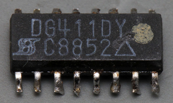
Siliconix DG411 contains four switches SPST-NO. You can buy DG412 with four NC or DG413 with two NO and two NC.

The DG411 can switch up to 40V while supplied with 44V. The resistance of the switch is 35 \$\Omega\$. Switching time is typically 100ns. Power consumption is less than 35µW.
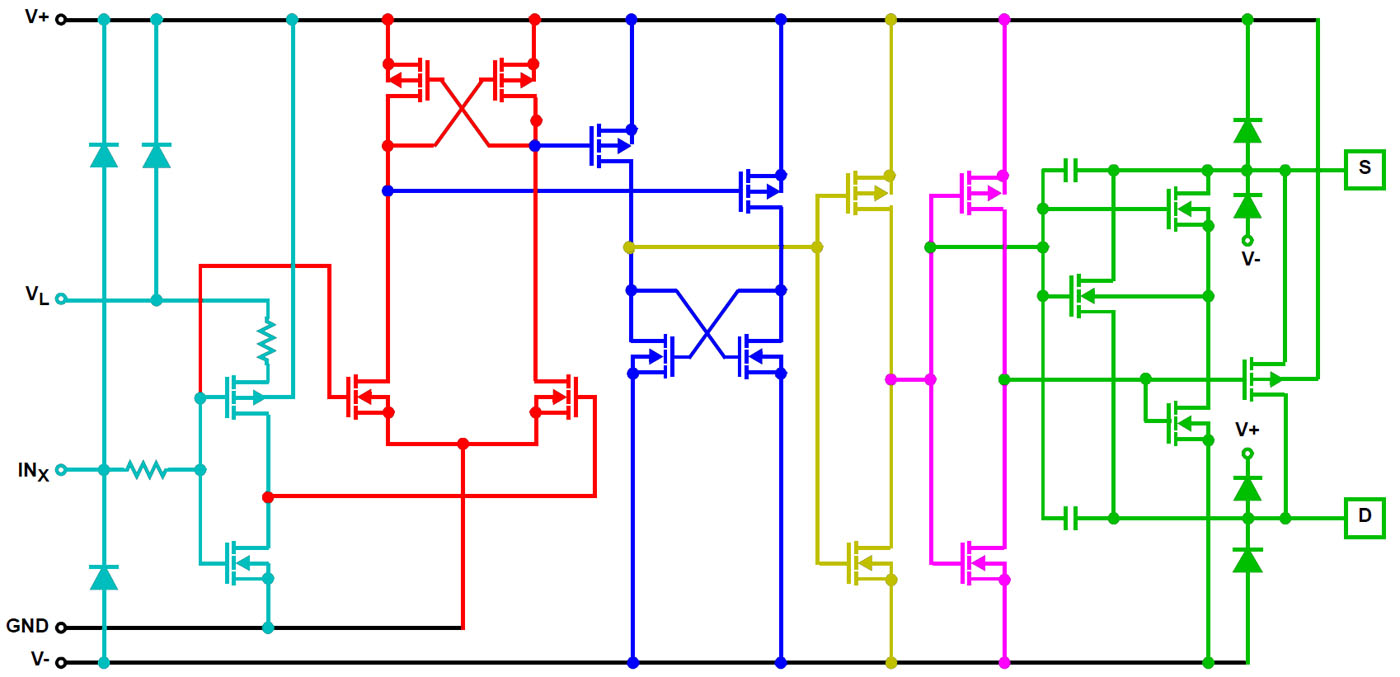


In the datasheet you can find a quite complete schematic. I have colored it.

The input stage can be driven with a different voltage level than the analog switch itself. There is an inverter in the first place (cyan). The input is protected with clamping diodes and a series resistor. There is an additional diode clamping VL against V+. That is important because the substrate is connected to V+. If there is a higher voltage than V+ there is current flow through the substrate.

The inverter generates a differential signal for the first differential amplifier (red). This amplifier converts the high level to V+. The second differential amplifier (blue) converts the low level to V-.

There are two inverters (yellow/pink). The first one probably can be bypassed to switch between a NO and a NC switch. We will talk about the analog switch itself later (green).
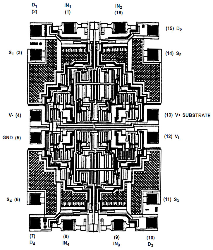


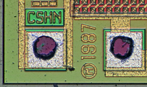
Datasheet contains a pictures of the metal layer. Datasheet states the size with 2760µm x 1780µm x 485µm. There is even a specification of the metal layer. It´s SiAl with a thickness of 1,2µm +/-0,1µm. Adding silicon is important so the aluminium doesn´t migrate into the silicon structures shorting them. Passivation is 0,8µm +/-0,1µm of silicon nitride.
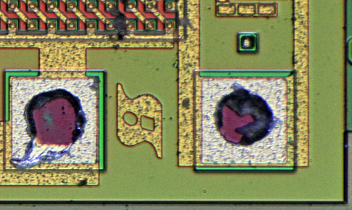


Siliconix :-+


Design is from 1987. CHSN could be initials of the developers.
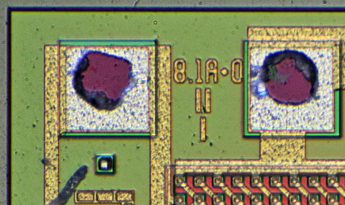


I assume switching between DG411, DG412 and DG413 was done by changing the metal layer. These characters could be markings for the different variants.
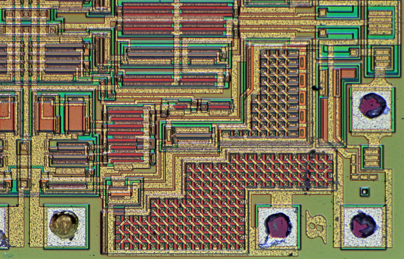


Except for the power supply there are four perfect symmetrical areas containing the four analog switches.

Most of the area is occupied by the two big transistors, the NMOS and the PMOS.
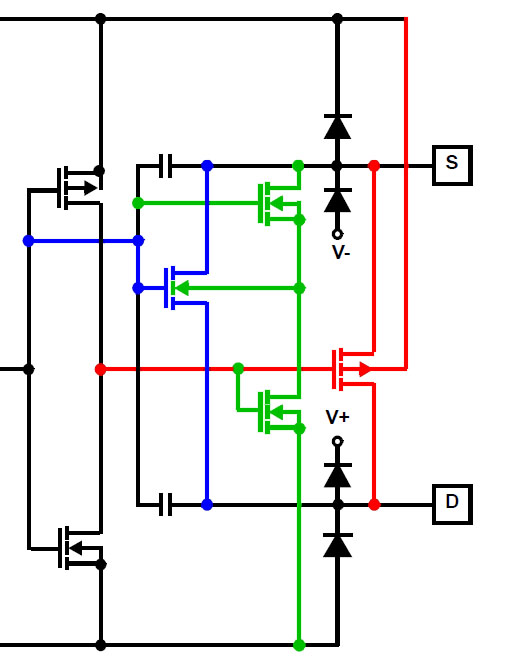


The analog switch itself looks quite complex but it isn´t. You have the NMOS (blue) and the PMOS (red). Bulk of the PMOS is connected to V+. Bulk of the NMOS is switched between the S pin and V- (green) like we have seen in the other analog switches.

We have clamping diodes to protect the structure.

I´m not sure why they have integrated the capacitors.  :-// I assume they stabilize the gate potential against the input signal.
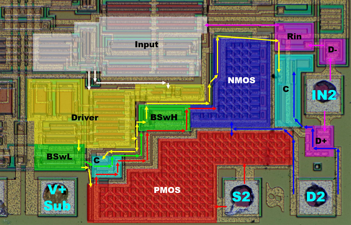


You can find nearly everything we talked about on the die. There are the protection diodes and the series resistor of the control input (pink).

There is the input stage supplied with VL and GND (white) and the rest of the driver stage (yellow) supplied V+ and V-.

You can find the two bulk switches (green) and the capacitos (cyan). One of the capacitors is bigger. That´s probably because on the other side there is one of the bulk MOSFETs increasing the capacitance of this path.

But there is no (clearly visible) protection diode at the input of the analog switch. That´s strange.  :o Of course it´s possible that these diodes are parasitic elements but I don´t see a straight path to the supply. That´s even more puzzling compared to the accurate input protection of the control input.


https://www.richis-lab.de/aswitch06.htm

 :-/O
« Last Edit: February 20, 2022, 08:04:44 am by Noopy »


Share me

Digg  Facebook  SlashDot  Delicious  Technorati  Twitter  Google  Yahoo
Smf