You need understand that every single piece of wire is inductor. Also inside your breadboard these GND and VCC routes are inductors (and also small capacitors).
Also this oscilloscope GND wire you connect to board GND. There wires are inductors.
As long as you are working with DC or low frequencies near DC and audio range and so on, these do dot matter anything or nearly nothing in practice.
Also even bit higher frequencies these do not matter so much when signals are somehow sinusoidal type.
But when we take higher frequencies these start matter more and more. Your square wave can be very low frequency, example 1kHz etc.. but there is these rising and falling edges. So there is also higher frequency components. These frequencies can very easy go to tens of MHz or more and even much more.
If you want thinking exercise. Draw our circuit to paper but do not draw wire and single wire but draw these as inductors and after then start thinking what happen there. And also not only these inductances but also there is capacitances. Probe tip may have example 15pF between tip and GND point.
Rough example this oscilloscope probe GND wire inductance can be 200nH
I can see there in your breadboard circuit some wires. You can roughly estimate that every 10mm of these wires may have 8nH inductance.
Now try estimate what is whole GND route inductance from GND jag to Teensy GND can estimate that it somewhere around 300nH
Example in your first message image there is CH3 trace. Rising edge ends to around very roughly ~60MHz oscillating. (overshoot)
And also note. These things you have now seen and displayed here. These all are normal. You have done this "magpies nest" circuit + probing.
And also note.
These have (in this case) nothing to with oscilloscope internal cross talk etc things. These all happen just externally, and thank your oscilloscope you can see what happens when probing have done wrong way.
When I look this same image 00002.png it looks like risetime is around 4ns +/-1ns
And when look your circuit and probe connection and specially with probe own long GND wire and also connected FAR away from pulse output GND and OUT... there is really nothing to wonder.
This single _probe_GND wire is around 200nH. Take your multimetes and tmeasure. Yes your meter tell it is 0 ohm.
But its reactance with example 60MHz is 75ohm! With 100MHz its reactance is 125 ohm. Not 0 ohm. Think about it. Every wire you have there, they are inductors. They have reactance. But then there is also capacitances - everywere. These all start effect when you have these signal rising and falling edges where you can easy find over 50MHz frequency components even if your square wave is 1kHz or even 1Hz or less. Only what matter is frequency components due to these "fast" edges.
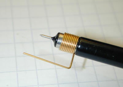
These kind of signals need look using short Signal and GND wires. Probe tip (not this hook) directly to output pin and probe GND directly to nearest possible GND point using GND spring or other contact there on signal source board. Many oscilloscope probes have small spring for do this contact (but example PB510 do not have).
Example your probe PB510 may have roughly 22pF input capacitance (when 10x)
If it is 22pF and GND wire inductance is 200nH and IF there is nothing else, its resonance is around 75MHz. And in your circuit there is more inductance via whole GND route related to signal output point.
And in these cases
both probes GND need of course connect. Because you are now working with tens of MHz RF signals not 1kHz or some audio. (due to signal edges)
You must NOT connect these using these long long GND wires if you want avoid these "weird" things you now wonder. These are natural in your circuit when you use probes like you have done. You are not working here with DC where short wire is just near 0 ohm.
It is sad that Siglent PB510 do not have these GND springs. But these are easy to do.
This is how you need use probe GND for better result.
https://www.eevblog.com/forum/testgear/needle-tip-oscilloscope-probes/msg798352/#msg798352