Author Topic: Transistors - die pictures  (Read 191773 times)

0 Members and 2 Guests are viewing this topic.

Offline NoopyTopic starter

  • Super Contributor
  • ***
  • Posts: 1739
  • Country: de
    • Richis-Lab
Re: Transistors - die pictures
« Reply #750 on: August 30, 2023, 09:21:47 am »
I agree with you, the 6W are questionable...  ???

Offline SeanB

  • Super Contributor
  • ***
  • Posts: 16284
  • Country: za
Re: Transistors - die pictures
« Reply #751 on: August 30, 2023, 10:39:01 am »
6W if you can just keep that base plate of the can at 25C, which is probably only possible when you have soldered it to a nice beryllium oxide washer, which in turn is on a nice Kovar heat spreader, cooled with Freon. Those TO39 cans normally had a finned heatsink, so can do 1W to 2W, depending on airflow, though I have seen them with clamp on heat spreaders that interfaced using a beryllia insulator to allow you to attach to a heatsink. Mil spec units, so price was not something they worried about, but they really wanted that TO39 package, but did not want to go full hybrid on it. We had some that had been reverse engineered, and those hybrids that came out were really nice, but the price per each was high.
 

Offline NoopyTopic starter

  • Super Contributor
  • ***
  • Posts: 1739
  • Country: de
    • Richis-Lab
Re: Transistors - die pictures
« Reply #752 on: September 17, 2023, 03:35:09 am »


The Philips BRY39 is described in the associated datasheet as a Programmable Unijunction Transistor and a Silicon Controlled Switch. It is a so-called thyristor tetrode. The properties of a thyristor tetrode are described in more detail in the context of the 3N84 (https://www.richis-lab.de/BipolarA40.htm). The BRY39 blocks up to 70V and conducts up to 175mA, briefly 2.5A, non-repetitively up to 3A.


The datasheet of the BRY39 shows the typical structure of a thyristor tetrode. It is a thyristor structure in which, in contrast to a thyristor or a programmable unijunction transistor, all four layers are contacted. However, a thyristor tetrode can of course be used as a thyristor or programmable unijunction transistor.


The dimensions of the die are 0,43mm x 0,42mm. There are auxiliary structures in the right-hand corners that make it possible to monitor the alignment of the masks. To the right of the innermost contact, you think you can see some damage. However, it seems to be just an artefact of the bond process and some dirt.


https://www.richis-lab.de/BipolarA40.htm

 :-/O
 
The following users thanked this post: SeanB, TurboTom, RoGeorge, Miyuki, ch_scr, karpouzi9

Offline NoopyTopic starter

  • Super Contributor
  • ***
  • Posts: 1739
  • Country: de
    • Richis-Lab
Re: Transistors - die pictures
« Reply #753 on: October 27, 2023, 06:29:44 pm »


The 2N2894 is a PNP transistor from National Semiconductor optimized for fast switching in the saturation region. Here you can see the bin with the index A, which is still a bit faster than the 2N2894. The A variant offers a cutoff frequency of at least 800MHz. The maximum turn-off time of 25ns is also worth mentioning. The blocking voltage is 12V. The current gain is typically 120 (150 for the 2N2894). The collector current must not exceed 200mA.


In the Discrete Databook from National Semiconductor there is a note that the 2N2984 is based on process 64. This is a process with a gold doping. Only transistors from process 65 (among others 2N4208) are faster, but with a maximum collector current of 50mA they are much less powerful.


If a bipolar transistor is operated in saturation, it contains very many free charge carriers. With an interruption of the base current, the number of free charge carriers is reduced continuously, but relatively slowly. As long as free charge carriers are still present, a collector current continues to flow. If you want to switch off bipolar transistors coming from the saturation region and you want to do it fast, you have to take additional measures to discharge free charge carriers. In the simplest case, the base and emitter are connected with a resistor through which the free charge carriers can exit the transistor. Such resistors are often found in Darlington transistors. Alternatively, the bipolar transistor can be driven with a push-pull stage to actively discharge the free charge carriers. In some cases it may be advantageous not to operate the transistor in saturation.

While manufacturing a transistor, one can optimize its intrinsic turn-off time by introducing gold doping. The gold atoms act as recombination points, which reduces the average lifetime of the free charge carriers. The IEEE article "Parasitic Effects in Microelectronic Circuits" deals with this technique. In this paper the influence of gold doping on parasitic effects is mainly considered, but the tables you can see here also show how the basic specifications are improved.

Process C contains gold doping and can be compared with process B, which has no gold doping. Process A lacks a buried collector. The lower table shows the reverse recovery times of the transistor junctions. The times are significantly shorter with gold doping. As a side effect, the leakage current into the substrate is also reduced, which is documented in the upper table. Due to the shorter lifetime, fewer free charge carriers reach the substrate.


It turns out that the structures on the die correspond to the illustration in National Semiconductor's Discrete Databook.


The transistor contains two emitter areas. The geometries could be interpreted as follows: The green area in the center contains the n-doping, which represents the base region. Within it are the two heavily p-doped emitter areas, which are hidden under the metal layer. The orange-red area represents the p-doped collector area, which is connected with low impedance to the substrate and to the package via a stronger, violet p-doping.


https://www.richis-lab.de/BipolarA41.htm

 :-/O
 
The following users thanked this post: SeanB, dzseki, SilverSolder, Wolfgang, RoGeorge, ch_scr

Offline NoopyTopic starter

  • Super Contributor
  • ***
  • Posts: 1739
  • Country: de
    • Richis-Lab
Re: Transistors - die pictures
« Reply #754 on: October 30, 2023, 05:06:00 pm »


The Siemens BSY34 is a fast switching transistor that was used to drive magnetic bubble memory. The dielectric strength is specified as 50V. The maximum collector current is 600mA. Besides a cutoff frequency of 400MHz, switching times of 30ns and 50ns respectively can be expected (tone/off). The BSY34 datasheet additionally lists the BSY58, which seems to be a slightly worse bin.


The die of the transistor is placed rotated by 45° between the pins of base and emitter. Neither the ball-wedge nor the wedge-wedge technique was used for the electrical connection. On the die, the bonding wires apparently already had the appropriate length before the bonding process. The wire was then welded to the metal surfaces on both sides. On the pins, the wire was processed in a similar way, but welded twice. It seems like the wires were cut off over the edges of the pins.


The edge length of the die is 0,60mm. The emitter surface describes the shape of a U. The fanned out base contact surrounds the emitter area and thus ensures a low-resistance connection to the active base area. In the lower right corner there are auxiliary structures which allow to evaluate the alignment of the masks against each other.


It can be assumed that heavily doped silicon was used in the BSY34 to achieve the high switching speeds. The low emitter base blocking voltage fits to this, which the datasheet specifies with 5V.

Here, the breakdown of the emitter base junction occurs at -6V and the well-known glow of the avalanche breakdown occurs. With increasing current, individual breakdown points change to a uniform glow over the whole junction. The current flow is 10mA, 20mA, 30mA and 50mA.


As described in detail in the context of the SF137 (https://www.richis-lab.de/Bipolar75.htm), the recombination of charge carriers can be observed in normal operation with the help of infrared imaging. The glow allows just a subjective comparison, yet it appears to be much more limited in the BSY34 than in the SF137. In the SF137, without collector current, the light extends far beyond the base contact.

With increasing collector current, the geometry of the glow appearance changes just slightly in the BSY34. However, there seems to be a slight shift towards the emitter, which would fit the shift of the recombination center of grarvity.

The optimization towards fast switching times could be an explanation for the more concentrated glow. If the free charge carriers are more concentrated in the active area, they probably can be discharged faster.


https://www.richis-lab.de/BipolarA42.htm

 :-/O
 
The following users thanked this post: SeanB, doktor pyta, Wolfgang, RoGeorge, ch_scr

Offline T3sl4co1l

  • Super Contributor
  • ***
  • Posts: 21701
  • Country: us
  • Expert, Analog Electronics, PCB Layout, EMC
    • Seven Transistor Labs
Re: Transistors - die pictures
« Reply #755 on: October 30, 2023, 07:42:56 pm »
Hmm, not so much heavily doped, given the modest breakdown voltages; gold doping likely though?

Could well be higher doping in the connection layers (by extension, substrate -- being the collector connecting layer -- if epitaxial type), forcing recombination near the junctions and reducing switching resistance.

(...Ah yes, "double diffused epitaxial", so that could be.  That is, n+ substrate; n- epitaxy for collector drift region; p (base) then n+ (emitter) diffusions; and, maybe p+ base contact diffusion?, but would that be triple, or can it be done at the same time as emitter?  Not sure.  ...Nah, don't think there's a base contact layer. That checks out then.)

Also I guess an extra "emitter" ring around everything, for guard ring?  I... forget exactly how those work, but that looks like what they've done anyway.

Tim
Seven Transistor Labs, LLC
Electronic design, from concept to prototype.
Bringing a project to life?  Send me a message!
 

Offline Wolfgang

  • Super Contributor
  • ***
  • Posts: 1775
  • Country: de
  • Its great if it finally works !
    • Electronic Projects for Fun
Re: Transistors - die pictures
« Reply #756 on: October 30, 2023, 07:48:35 pm »
Unglaublich saubere Fertigung. für das Alter. Haben wir Restströme von dem Ding ?
In English, sorry: Very clean manufacturing, indeed. Do we have leakage currents for this part ?
« Last Edit: October 30, 2023, 11:06:19 pm by Wolfgang »
 

Offline NoopyTopic starter

  • Super Contributor
  • ***
  • Posts: 1739
  • Country: de
    • Richis-Lab
Re: Transistors - die pictures
« Reply #757 on: October 30, 2023, 09:11:42 pm »
Hmm, not so much heavily doped, given the modest breakdown voltages; gold doping likely though?

A modest Vce but the Veb is quite low with 5V. Nevertheless, of course there are HF transistors with higher doping concentration.
Gold doping is at least possible but you don´t find a hint in the datasheet.


Could well be higher doping in the connection layers (by extension, substrate -- being the collector connecting layer -- if epitaxial type), forcing recombination near the junctions and reducing switching resistance.

(...Ah yes, "double diffused epitaxial", so that could be.  That is, n+ substrate; n- epitaxy for collector drift region; p (base) then n+ (emitter) diffusions; and, maybe p+ base contact diffusion?, but would that be triple, or can it be done at the same time as emitter?  Not sure.  ...Nah, don't think there's a base contact layer. That checks out then.)

I agree with your explanation.


Also I guess an extra "emitter" ring around everything, for guard ring?  I... forget exactly how those work, but that looks like what they've done anyway.

Since the "emitter ring" is in the collector area it generates no real junction. But probably it hat a positive effect...


Unglaublich saubere Fertigung. für das Alter. Haben wir Restströme von dem Ding ?

Hello Wolfgang! Some german words?  ;)
The cutoff current is at room temperature <70nA (Vcbo=50V).
Really a nice transistor.  8)

Offline Wolfgang

  • Super Contributor
  • ***
  • Posts: 1775
  • Country: de
  • Its great if it finally works !
    • Electronic Projects for Fun
Re: Transistors - die pictures
« Reply #758 on: October 30, 2023, 11:07:16 pm »
I see a datasheet leakage of 70nA maximum, but I am sure its in the picoamps when measured. Any measurements available ?
 

Offline NoopyTopic starter

  • Super Contributor
  • ***
  • Posts: 1739
  • Country: de
    • Richis-Lab
Re: Transistors - die pictures
« Reply #759 on: October 31, 2023, 12:09:19 pm »
DMM6500 says 30nA @40V.
But I had to take the open part because I have just this one. It is now open for some days, let´s say one or two weeks.
I tried to keep the transistor away from light.
 
The following users thanked this post: SeanB

Offline Wolfgang

  • Super Contributor
  • ***
  • Posts: 1775
  • Country: de
  • Its great if it finally works !
    • Electronic Projects for Fun
Re: Transistors - die pictures
« Reply #760 on: October 31, 2023, 10:43:55 pm »
Thanks, I will try to get some parts that are still in their can. Opening normally kills leakage current due to moisture and other gases.
Where did you get your parts from ?
 

Offline NoopyTopic starter

  • Super Contributor
  • ***
  • Posts: 1739
  • Country: de
    • Richis-Lab
Re: Transistors - die pictures
« Reply #761 on: November 01, 2023, 03:54:38 am »
Thanks, I will try to get some parts that are still in their can. Opening normally kills leakage current due to moisture and other gases.
Where did you get your parts from ?

I agree with you.

Unfortunately my contact doesn´t sell any more:
https://www.ebay.de/itm/386171199806
 :(

Offline Wolfgang

  • Super Contributor
  • ***
  • Posts: 1775
  • Country: de
  • Its great if it finally works !
    • Electronic Projects for Fun
Re: Transistors - die pictures
« Reply #762 on: November 01, 2023, 11:38:52 am »
Dont worry, it was me who bought the rest  ^-^
 

Offline NoopyTopic starter

  • Super Contributor
  • ***
  • Posts: 1739
  • Country: de
    • Richis-Lab
Re: Transistors - die pictures
« Reply #763 on: November 02, 2023, 02:15:56 pm »


The SSY20 built by the Halbleiterwerk Frankfurt Oder was developed as an alternative to the BSY34 for use in magnetic bubble memory. The specifications are accordingly similar. The SSY20 blocks 40V and conducts up to 600mA. The switching times of 50ns and 100ns (tone/off) respectively are somewhat longer than those of the BSY34. PL stand for a production in December 1971.


The edge length of the die is 0,7mm. On the surface there are some major scratches. The active structures remind of the structure of power transistors. In the lower left corner there is a geometry that allows to check the alignment of the masks.


The breakdown of the base-emitter junction occurs at -9,4V. In the images seen here, the current increases from 10mA to 50mA in 10mA steps. The luminescent effect appears uneven, suggesting that the structures are somewhat inhomogeneously built or contain imperfections.


The recombination of free charge carriers emits light in the infrared range, which makes it possible to visualize the recombination centers. We had that before. However, the distribution of the light islands and their luminances are not particularly informative for the SSY20.


Here you can see another SSY20 transistor, also produced in December 1971.


The design and structures are basically the same. However, there is significant damage in the lower area of the transistor. The visual appearance of the defect and its location suggest that it is not caused by an electrical overload but was more likely a weakness in the production.


This transistor is not labeled, but it is known that it is also an SSY20.


The design is similar to the design of the already documented SSY20 transistors. Here, the first bond process at the emitter was obviously not successful.


Here you can see the structure of another unlabeled SSY20 transistor.


The bond quality in this transistor is also not ideal. At the base potential (left) the area next to the bondwire is severely damaged. According to the optical appearance, a bond process took place there, during which the bondwire came loose again. In the lower right area of the transistor, the metal layer is heavily scratched, which could also have happened during the bond process.


The breakdown of the base-emitter path occurs earlier in this model, at -6,5V. The currents here are 10mA, 20mA, 50mA, 100mA and 200mA. Despite the damage, the light distribution is still relatively even.


The collector-base junction can also be driven in avalanche at 77,5V. The current flow in this picture is just 10mA. However, that´s already a power dissipation of 7,8W, which is why this operating point can only be reached for a very short time.

As with the base-emitter breakdown, a light effect occurs with the collector-base breakdown too. The documentation of the 2N2857 (https://www.richis-lab.de/Bipolar16.htm) has shown how clear this effect can be. In the SSY20, only a small point lights up in the right area of the lower edge.


https://www.richis-lab.de/BipolarA43.htm

 :-/O
 
The following users thanked this post: SeanB, RoGeorge, ch_scr

Offline T3sl4co1l

  • Super Contributor
  • ***
  • Posts: 21701
  • Country: us
  • Expert, Analog Electronics, PCB Layout, EMC
    • Seven Transistor Labs
Re: Transistors - die pictures
« Reply #764 on: November 02, 2023, 09:48:42 pm »
Sheesh, feels like a couple of those were bonding practice! :-DD

Tim
Seven Transistor Labs, LLC
Electronic design, from concept to prototype.
Bringing a project to life?  Send me a message!
 

Offline NoopyTopic starter

  • Super Contributor
  • ***
  • Posts: 1739
  • Country: de
    • Richis-Lab
Re: Transistors - die pictures
« Reply #765 on: November 03, 2023, 11:04:22 am »
Yeah, they definitely had some problems getting the bonds robust.  :palm:

I had one minor mistake:
The BSY34 and the SSY20 were designed for ferrite core memory, not for magnetic bubble memory.

Offline NoopyTopic starter

  • Super Contributor
  • ***
  • Posts: 1739
  • Country: de
    • Richis-Lab
Re: Transistors - die pictures
« Reply #766 on: November 05, 2023, 08:06:29 pm »


The 2N2646 is a unijunction transistor. In contrast to the so-called programmable unijunction transistors such as the 2N6027 (https://www.richis-lab.de/Bipolar14.htm), the 2N2646 is a real unijunction transistor, i.e. it contains just one junction. A manufacturer cannot be determined. The numbers 0248 could be a date code. The component would therefore have been manufactured in 2002.


The pictures above are taken from the book "Beyond the Transistor: 133 Electronics Projects" and show, among other things, the structure of a unijunction transistor. It consists of an n-doped elongated element. The ends of this element are labelled base1 and base2. A p-type doping is inserted and contacted at the side. This connection is called the emitter. The n-doped element represents two resistors, between which a diode is formed at the emitter connection. If a voltage is applied between the two base connections, a certain potential is established at the emitter depending on the position of the p-doping.

The characteristic curve is shown in simplified form. It shows the voltage Ve between the emitter and the lower base as a function of the emitter current. The behaviour is easier to understand if Ve is varied and the resulting current is observed. As long as the potential applied to the emitter from the outside is lower than the potential set by the voltage divider between base 1 and base 2, the pn junction is isolating the emitter. Just a very small leakage current (1-2) flows into the emitter. If the pn junction becomes conductive, more current can flow into the emitter. At first glance, the behaviour of the voltage Ve is unusual, as it decreases in this area as the current increases (2-3).

There is only n-doped material between the base contacts. The current flow in the first part of the characteristic curve can therefore only take place via free electrons. As soon as current flows into the emitter, additional positive charge carriers ("holes") flow from the p-doped area into the unijunction transistor. The additional transport mechanism reduces the resistance between the base contacts.

The unijunction transistor can therefore represent a negative resistance. This feature was used in the past to build oscillators with little component effort. Another advantage was certainly that the structures are less complicated than those of a transistor and were therefore probably easier to manufacture.


In February 1968 (Volume 41), the journal Electronics describes the development of the design. The first unijunction transistors consisted of an n-doped cuboid into which the emitter contact and thus a p-doping was alloyed at the same time. This principle was further improved until the unijunction transistors could be manufactured using planar technology and finally integrated with other circuit components.


This 2N2646 contains a modern-looking die. What is unusual is that the bond connections on the pins have been additionally protected with a type of varnish.


The edge length of the die is 0,45 mm. A manufacturer cannot be determined here either. Just the Cyrillic letters КБB (KBV) in the top right-hand corner provide a clue. For the simple design of a unijunction transistor, the structures on the die are surprisingly complex.


It is certain that the emitter is contacted from the left and the base1 from the right. The potential of base 2 is tapped via the housing, i.e. via the substrate. The reddish area under the emitter contact must contain a p-type doping. It appears that three possible emitters have been integrated here. There must be a strong n-doping under the smaller central base contact, which ensures a low-resistance connection of the n-doped area. On closer inspection, you can see that the three possible emitters have different distances to the base 1 contact. If the emitter bondwire is placed differently, the properties of the component can be modified.

The contact in the bottom left-hand corner appears to be relatively deep. It is most likely a connection to the substrate and therefore to base2. Thin lines lead to the emitter areas. Probably the lines makes it possible to connect unused emitter areas to the base2 potential. The low base2 potential guarantees that no charge carriers flow from the inactive emitter surfaces into the active area.


https://www.richis-lab.de/BipolarA44.htm

 :-/O
 
The following users thanked this post: SeanB, doktor pyta, TurboTom, SilverSolder, RoGeorge, ch_scr

Offline NoopyTopic starter

  • Super Contributor
  • ***
  • Posts: 1739
  • Country: de
    • Richis-Lab
Re: Transistors - die pictures
« Reply #767 on: November 11, 2023, 08:03:13 pm »


The BC109 is a low-noise transistor from the first generation of the BCxxx family. The maximum collector emitter voltage is 25V. Collector currents of up to 200mA are permissible. The cut-off frequency is specified at more than 100MHz. The amplification factor of the transistors lies between 200 and 800, with index B limiting the range to 200-450. The manufacturer of this transistor cannot be identified.


The dimensions of the die are 0,40mm x 0,39mm. The base contact only covers half of the emitter area.


https://www.richis-lab.de/BipolarA45.htm

 :-/O
 
The following users thanked this post: SeanB, RoGeorge, ch_scr

Offline NoopyTopic starter

  • Super Contributor
  • ***
  • Posts: 1739
  • Country: de
    • Richis-Lab
Re: Transistors - die pictures
« Reply #768 on: November 20, 2023, 03:49:59 am »


The КT117 is a unijunction transistor, as described in more detail in the 2N2646. The logo belongs to the Russian Ulyanovsk radio tube plant and had to be rotated 90° anti-clockwise on the small housing. The index, here a B (Latin V), shows which resistance can be expected between the two base connections. There are a total of four bins with two different resistance values and two different factors by which the resistance value can change.


The housing contains a die with an edge length of 1,13 mm. A transparent potting protects the semiconductor.


This is the classic structure of a unijunction transistor, as documented in the 2N2646. The bottom of the n-doped substrate represents the base contact B1. The right-hand bondpad forms the second base contact. The left-hand bondwire transmits the emitter potential.

At first glance, one might have thought that the right-hand area was the p-doped emitter. This is obviously not the case here. No edge can be recognised around the emitter bondpad. It can therefore be assumed that the entire area around the bondpad B2 contains a p-type doping. Two frame structures can be recognised under and next to the base bondpad. Low-resistance contacting of an n-doped surface requires a local strong n-doping. The inside of the two edges shows the area that contains this stronger n-doping. The outer edge is a window within the emitter surface and exposes the n-doped substrate. The outer frame most likely contains an n-doping and thus represents a clean termination of the emitter surface.


https://www.richis-lab.de/BipolarA46.htm

 :-/O
 
The following users thanked this post: SeanB, RoGeorge

Offline NoopyTopic starter

  • Super Contributor
  • ***
  • Posts: 1739
  • Country: de
    • Richis-Lab
Re: Transistors - die pictures
« Reply #769 on: November 23, 2023, 08:24:38 pm »


The PNP germanium transistor AF201 built by Siemens is a high-frequency transistor with a cut-off frequency of at least 100 MHz. The blocking voltage is 25V. The maximum permissible collector current is 10mA. The AF201 can dissipate up to 225mW. The junction temperature must not exceed 90°C.

The AF200 is also described on the same datasheet. The AF200 and the AF201 are obviously two grades of the same transistor type. The guaranteed current amplification of the AF201 is slightly lower than that of the AF200 at a factor of 20 and the feedback capacitance is slightly higher (maximum 0,7pF).


The housing contains a white compound that protects the structures from environmental conditions and improves heat dissipation towards the housing.


The AF201 has four pins. In addition to the collector, base and emitter, one pin contacts the housing exclusively. The transistor is located on a carrier insulated from the housing, which is welded to the collector pin.


A kind of protective lacquer is applied to the die. Due to the varying thickness of the lacquer, the interferences in the layer create a repeating rainbow pattern. The edge length of the die is 0,5mm. The structure of this type of high-frequency transistor is described in more detail in the 2N1561 (https://www.richis-lab.de/BipolarA47.htm). The area around the active area has been etched down so that just a pedestal with an edge length of 0,1 mm remains. This measure reduces the parasitic capacitances. The base is diffused into the pedestal. On top of the pedestal is a base contact and the emitter, both alloyed into the base.


https://www.richis-lab.de/BipolarA47.htm

 :-/O
 
The following users thanked this post: SeanB, SilverSolder, RoGeorge, Miyuki, 42Khz

Offline NoopyTopic starter

  • Super Contributor
  • ***
  • Posts: 1739
  • Country: de
    • Richis-Lab
Re: Transistors - die pictures
« Reply #770 on: December 06, 2023, 04:57:42 am »


Here you can see the germanium power transistor OC864A, which was developed in the Funkwerk Erfurt but never went into series production. Only a few sample exist in the Thuringian Museum of Electrical Engineering (https://www.elektromuseum.de). The following background information also comes from this museum.

In 1959, the VEB Funkwerk Erfurt (FWE) ceased production of transmitter tubes. The capacities freed up were used to start developing germanium power transistors in the so-called Zentrallabor für Empfängerröhren (ZLE). An important basis for this work was a Soviet documentation. In addition to the necessary dimensions of the germanium crystal, it described how to etch the material, which alloy materials to use and which geometries to aim for. Alloying was carried out in a graphite mould under vacuum. The design of the alloying furnace was also taken from the Soviet documentation. However, the optimum temperatures and times for the alloying process were missing and had to be determined from tests. At the end of 1962, after the development had been completed, the results were transferred to the Halbleiterwerk Frankfurt Oder (HFO).


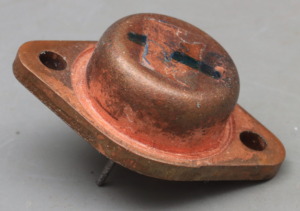
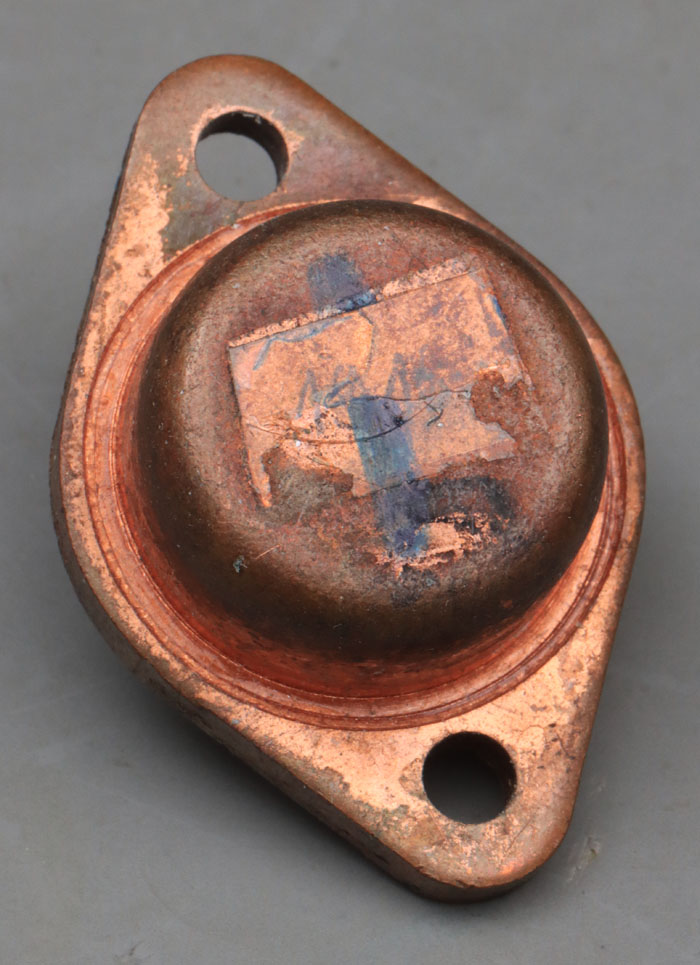
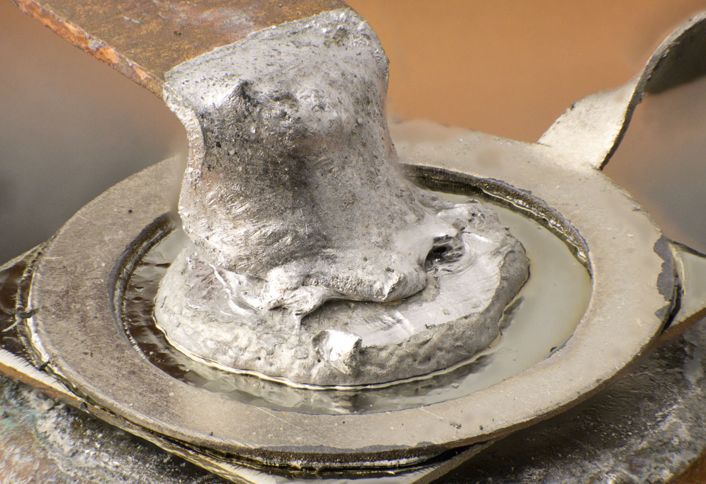
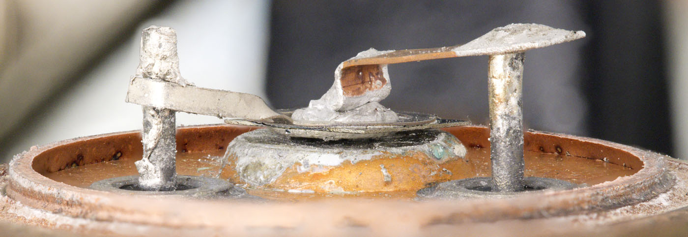
The transistor housing is made of copper. The base plate is 3 mm thick.


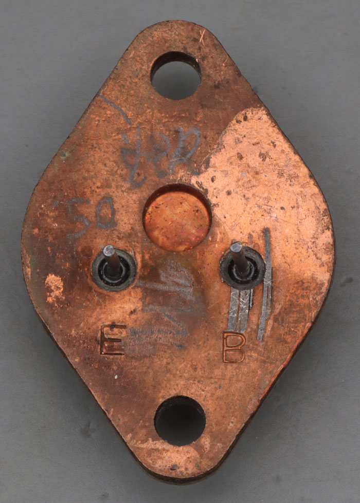
Letters are stamped into the base plate to identify the pins for the base and emitter. The indentation creates a socket on the top, on which the actual transistor is located.


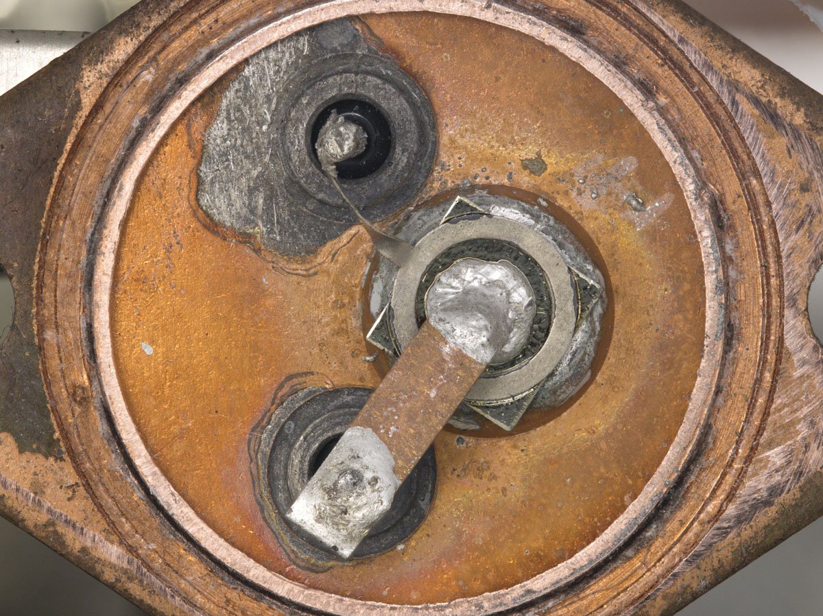
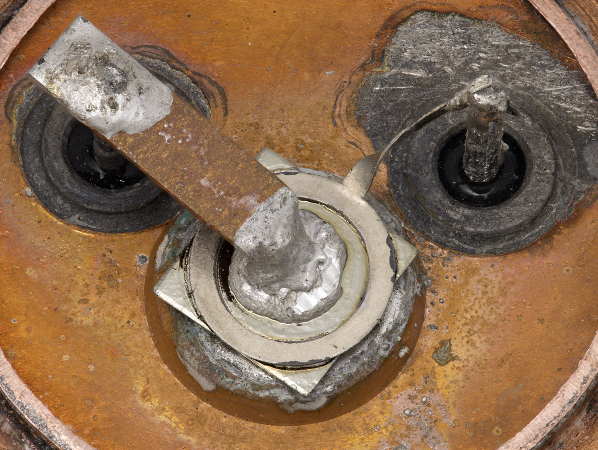
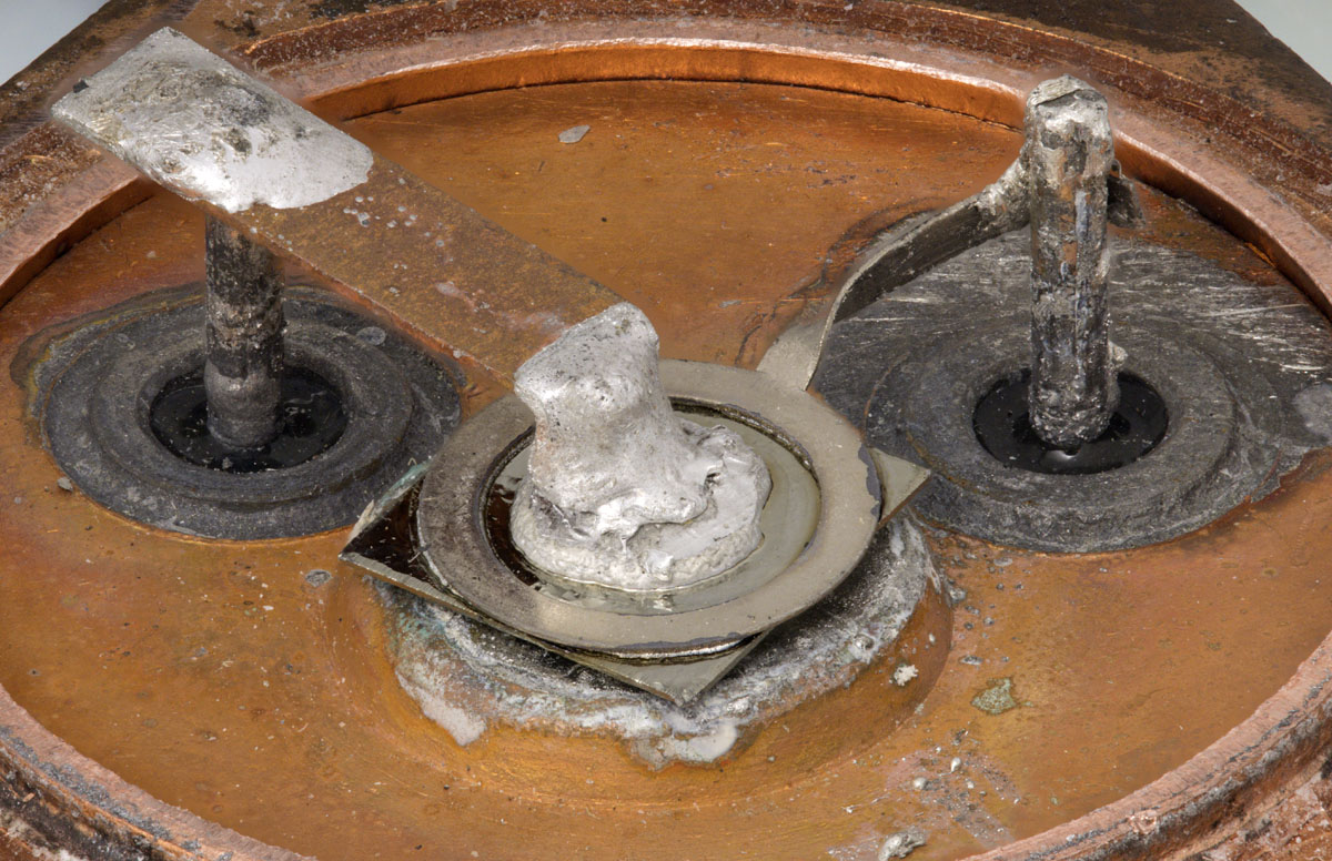
The construction and connection technology is not unusual for a germanium power transistor. A ring-shaped electrode contacts the germanium platelet and thus transmits the base current. The emitter current is supplied in the centre.


The quality of the solder connection between the base pin and the contact plate is very poor.


The germanium crystal has an edge length of 5,6mm. An edge length of 6mm should enable a power dissipation of 25W. An edge length of 4mm was intended for 15W transistors.


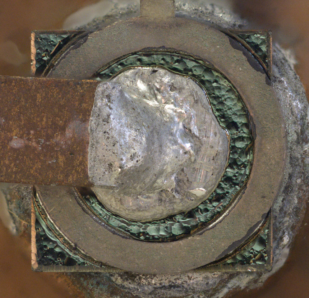
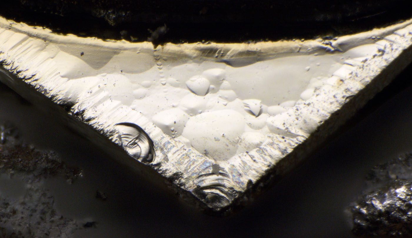
To produce the emitter shown here, an indium-gallium mixture was alloyed into the germanium. Pure indium was used at the collector. It is easy to recognise that there are two metal layers on the germanium platelet. The lower element is the alloy material that forms the emitter. The emitter contact was soldered onto this with a solder that melts at a low temperature.


The germanium disc was manufactured at the Halbleiterwerk Stahnsdorf, which belonged to VEB Halbleiterwerk Frankfurt Oder (HFO). The surface shows the familiar structure resulting from the etching process used to clean the surface. The edges appear to have been reworked in some way. The surface structure changes in these areas.


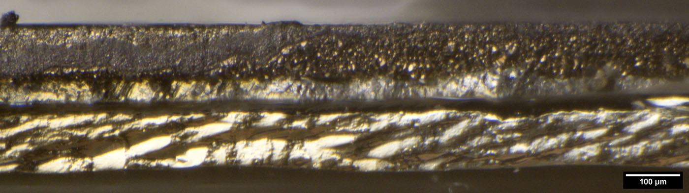
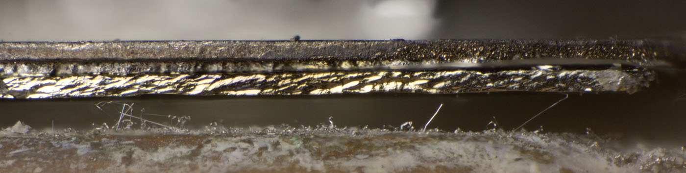
The germanium disc is approximately 0,12 mm thick. There is a 0,05mm thick solder layer and the 0,10mm thick base electrode.


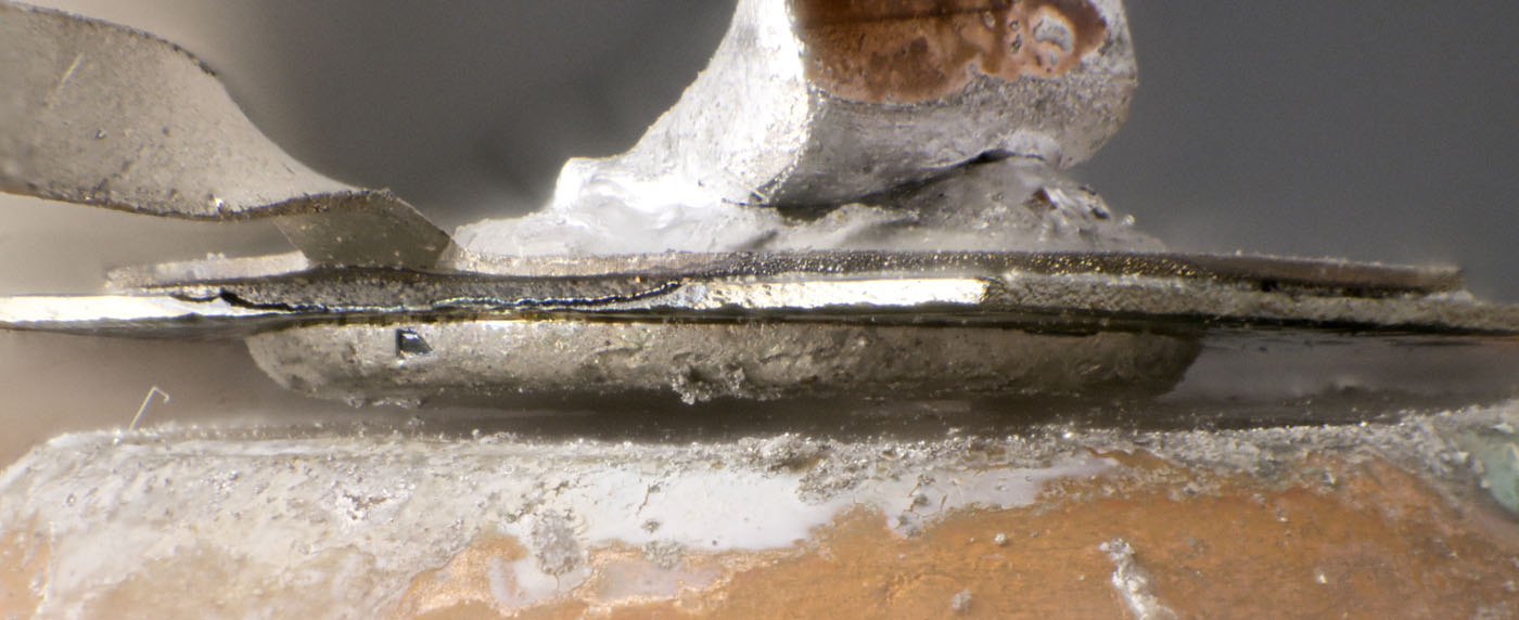
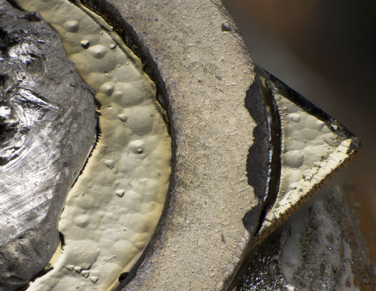
The transistor does not lie completely flat on the socket of the base plate. This allows a better view of the collector area. The alloy material, which covers a larger area on the collector than on the emitter, is clearly visible. Very little solder appears to have been used for the collector connection. With such a small contact area, it is difficult to dissipate the transistor's power loss. In order to obtain high-quality transistors, this process would definitely need some optimization.


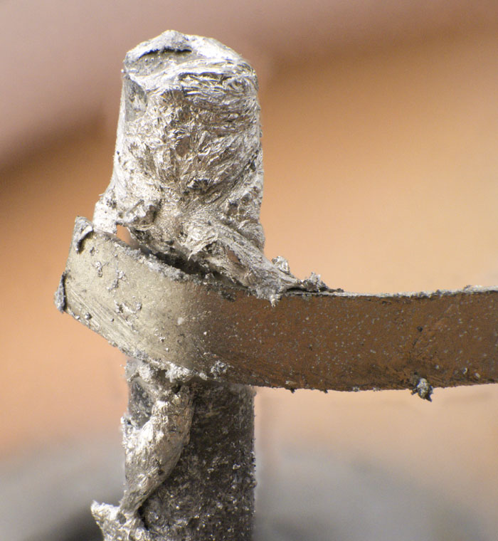
On closer inspection, you can see that so-called whiskers that have formed on the base. This is usually tin, which forms such crystal structures over time under certain circumstances. These whiskers can cause short circuits.


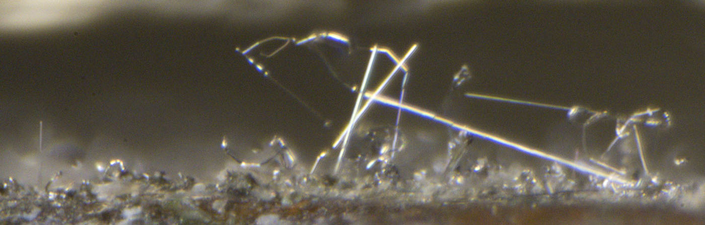
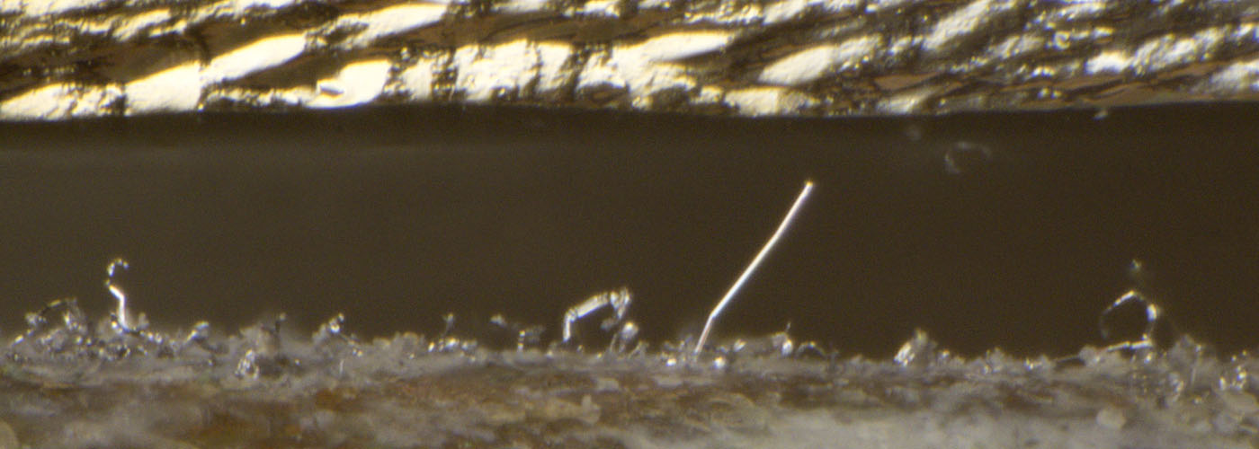
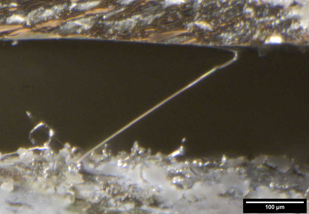
The diameter of the whiskers is just 5µm. There appears to be a complete connection between collector and base.

Some of the images also show small dendrites, as were found much more extensively in GD241 (https://www.richis-lab.de/BipolarA12.htm).


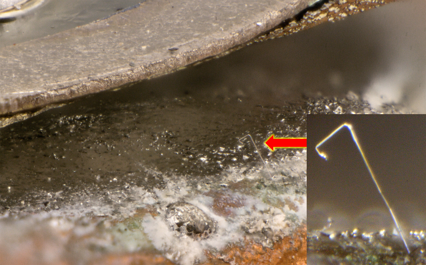
The overview image shows the proportions once again. It could be that the whisker had caused a short circuit, which then was melted by a current flow. This would explain the thickening at the end of the whisker.


https://www.richis-lab.de/BipolarA48.htm

 :-/O
 
The following users thanked this post: SeanB, Gyro, RoGeorge, ch_scr, mawyatt, rteodor

Offline NoopyTopic starter

  • Super Contributor
  • ***
  • Posts: 1739
  • Country: de
    • Richis-Lab
Re: Transistors - die pictures
« Reply #771 on: December 06, 2023, 05:26:57 am »
By the way: In the background that are 1250 pictures, which occupy 60GB on my network storage...  ;D
 
The following users thanked this post: SeanB, MegaVolt

Offline pickle9000

  • Super Contributor
  • ***
  • Posts: 2439
  • Country: ca
Re: Transistors - die pictures
« Reply #772 on: December 06, 2023, 05:34:18 am »
Awesome!
 
The following users thanked this post: Noopy

Online RoGeorge

  • Super Contributor
  • ***
  • Posts: 6213
  • Country: ro
Re: Transistors - die pictures
« Reply #773 on: December 06, 2023, 12:04:11 pm »
Interesting story, beautiful pics, thanks!  :-+

Just out of curiosity, estimating R of a tin whisker:
R = \$\rho\$*L/S
\$\rho_{\mathrm{Sn}}\$ = 10.9E-8\$\Omega\$*m
L = 0.1mm
d = 5um

R = 10.9E-8 * 0.1E-3 / (3.14 * 25E-12 / 4) = 1.09/(3.14*1.25) = roughly 1/4 = 0.25\$\Omega\$  ???

I was expecting a much bigger R from such a thin wire.
 
The following users thanked this post: Noopy

Offline MegaVolt

  • Frequent Contributor
  • **
  • Posts: 918
  • Country: by
Re: Transistors - die pictures
« Reply #774 on: December 06, 2023, 12:08:01 pm »
I was expecting a much bigger R from such a thin wire.
It burns very easily turning into plasma. But the plasma channel has low resistance.
 
The following users thanked this post: Noopy


Share me

Digg  Facebook  SlashDot  Delicious  Technorati  Twitter  Google  Yahoo
Smf