-
I got the G, S, D part.
Simply so that they are large enough to actually make a connection into the Real World.
but what are end pads? and why do you scale up from nm to um as you move top the layers?
Contact pads that seem as large as an aircraft carrier (when viewed from the perspective where you can "see" individual transistors) are barely visible in the Real World unless viewing through a microscope.
We once printed out the die layout of a CPU chip (386 IIRC) so that it was 30 feet across. The bond pads were something around 4 inches 100mm square and the plot filled one wing of the cafeteria. But even at that resolution, the individual transistors weren't really visible. They were only 2-3 pixels in size. -
There are these two classic images by, if I'm not mistaken, intel and IBM:
Intel, 11 metal layers. Clearly shows how metals are getting thicker. Green is a low-k dielectric, used to reduce capacitance (due to the high \$\epsilon_{R}\$ of silicon, the parasitic capacitance would be very high if SiO would be used all the way to the top layers): ...
This is mind bogglingly amazing!!
How on earth do you get such great images?!
Interesting thing that you talk about the repeatable pattern. And there also seems to be a pattern on the upper half of the thick substrate layer (the bottommost one).
What patterns are those?
Are the substrate and the 2 layers above it, the transistors?
With regards to the bottom most image what kind of program generates such kind of design, is it a CAD program or a specialized IC design software?
Also, when do you use polysilicon and when do you use metal, I guess both thes are used for interconnects right? -
There are these two classic images by, if I'm not mistaken, intel and IBM:
Intel, 11 metal layers. Clearly shows how metals are getting thicker. Green is a low-k dielectric, used to reduce capacitance (due to the high \$\epsilon_{R}\$ of silicon, the parasitic capacitance would be very high if SiO would be used all the way to the top layers): ...
This is mind bogglingly amazing!!
How on earth do you get such great images?!
Interesting thing that you talk about the repeatable pattern. And there also seems to be a pattern on the upper half of the thick substrate layer (the bottommost one).
What patterns are those?
Are the substrate and the 2 layers above it, the transistors?
The transistors are completely in the bottom layers. For a planar process (bulk CMOS, not FINFET), the transistors look like this (source):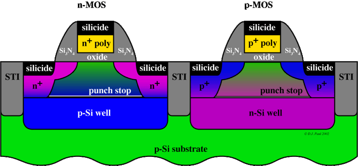
This is all made before the first metal layer is deposited. There are some small differences between processes (metalgate, self-aligned transistors) but that would take us too far. Everything is built out of the original silicon, with exception of the two bumps. After this is made (everything up to this point is called front-end-of-line) we start with metals (back-end-of-line).
Fin-Fets, which is what you see in the second picture, involves growing fins. It's these fins I think you are talking about.
No metals are involved in making the actual transistors, they are only used after the transistors are made, to connect them to each other (exception would be metal-gate, but again, details that are not important now).
With regards to the bottom most image what kind of program generates such kind of design, is it a CAD program or a specialized IC design software?
When we design such a thing we use a combination of tools: Cadence Layout (G)XL (to do the actual drawing of materials), Keysight EEsof ADS/momentum (first, fast simulations of simpler structures), Ansys HFSS (detailed high-performance analysis of EM stuff), Mentor Calibre (Layout-vs-schematic and parasitic-extraction, though the latter isn't that usefull anymore to us, since we simulate with EM simulators). It is all hand-drawn, there isn't some auto-generator for it.
To get the nice 3D plot: I believe the university of Twente has a nice 3D GDSII viewer, which is often used for that. Mind you, apart from making nice images for publications and such we don't tend to use it much.
-
Fin-Fets, which is what you see in the second picture, involves growing fins. It's these fins I think you are talking about.
Is the second picture in the link you provided because I don't see it in the post? -
The transistors are completely in the bottom layers. For a planar process (bulk CMOS, not FINFET), the transistors look like this (source):
This is all made before the first metal layer is deposited. There are some small differences between processes (metalgate, self-aligned transistors) but that would take us too far. Everything is built out of the original silicon, with exception of the two bumps. After this is made (everything up to this point is called front-end-of-line) we start with metals (back-end-of-line).
1. For NMOS why make a p-Si well when a P-Si already exists?
2. What is punch stop?
3. What is STI?
4. The silicide layers are used as conductors? But then why the gate has n+poly also where as the drain and source has only silicide and no n+ poly?
I guess I'll do some searches on the internet and see what answer each of those questions return?
-
The main reason is that the doping profile of each well can be individually tailored. Also provides isolation benefits
The transistors are completely in the bottom layers. For a planar process (bulk CMOS, not FINFET), the transistors look like this (source):
This is all made before the first metal layer is deposited. There are some small differences between processes (metalgate, self-aligned transistors) but that would take us too far. Everything is built out of the original silicon, with exception of the two bumps. After this is made (everything up to this point is called front-end-of-line) we start with metals (back-end-of-line).
1. For NMOS why make a p-Si well when a P-Si already exists?Quote2. What is punch stop?
Not sureQuote3. What is STI?
Shallow Trench Isolation
This technique replaces the old LOCOS techniqueQuote4. The silicide layers are used as conductors? But then why the gate has n+poly also where as the drain and source has only silicide and no n+ poly?
Yes, silicide is a refractory metal--a conductor.
Polysilicon is the preferred material to make defect-free gates. Metal is terrible as the gate-oxide interface
There is no need for poly at the source and drains. -
Just a few questions that come to my mind while contemplating on the topic
1. Why is the silicon wafer when its being manufactured from a liquid kind of state not 100% pure silicon?. Why is it doped to become an N type or a P Type substrate? I mean some dopants are added to the mix when the wafer is being manufactured?
2. Why is an epitaxial coating done over the silicon wafer before any other processes are done?
3. Is there a comprehensive list of steps for silicon chip fabrication?
TIA -
Just a few questions that come to my mind while contemplating on the topic
1. Why is the silicon wafer when its being manufactured from a liquid kind of state not 100% pure silicon?. Why is it doped to become an N type or a P Type substrate? I mean some dopants are added to the mix when the wafer is being manufactured?
This is a deep and involved topic with lots of history.
Lets work backwords from the transistor structure.
An N-channel transistor needs N+ source and drain (the "+" indicates heavy doping of donor atoms) diffused into silicon doped with acceptor atoms so that the underlying material is doped P type. In order to achieve desired transistor performance, that material is very lightly doped...we call it P- where the "minus" means lightly doped. In the above, Phosphorous is typically used as a donor dopant, and Boron is used as an acceptor dopant.
If all you wanted to build were N-channel transistors, you could manufacture a silicon wafer that has a P- doping. In fact, early MOS technology was either totally N-channel, or totally P-channel. Of course, for a totally P-channel circuit, the wafer would have to be manufactured with N- doping.
Wafers come from silicon ingots, or boules, that are manufactured using the Czochralski method. Molten silicon is gradually extracted starting with a crystalline seed. For doping requirements, the molten silicon can be doped with donors or acceptors to achieve the desired doping.
Nobody uses NMOS, or PMOS any more. CMOS instead!! So, how do you put a p-channel transistor in a wafer that is already doped P- ??
Well, you have to create regions on the wafer that are lightly doped N-. These regions are called "wells." So, for CMOS, you may start with a lightly doped P- wafer as the basic substrate, then create well that is doped N- (either by ion implantation, or diffusion, or combination of both). Withing the n-well, you can put p-channel transistors. In the regions outside of the well, you can put the n-channel transtors. Now you have CMOS!!
That is pretty much it, except for about a million other details.Quote2. Why is an epitaxial coating done over the silicon wafer before any other processes are done?
Epi layers can be created with more precise and tuned properties than can be achieved with the C-growth method. The underlying substrate can be high conductivity enabling better performance under certain condition.Quote3. Is there a comprehensive list of steps for silicon chip fabrication?
Yes. Have you googled for this?
Also, the processing steps of changed over the years-- metal-gate, silicon-gate, oxide-isolated, shallow-tranch isolation, on and on...
Go here: https://aicdesign.org/wp-content/uploads/2018/08/lecture02-131209.pdf -
3. Is there a comprehensive list of steps for silicon chip fabrication?
https://en.wikipedia.org/wiki/Semiconductor_device_fabrication#List_of_steps
That is as good as you are going to get if you are asking for a list of generic types of processes.
If you are asking about the exact steps for a particular device or fab process, that is typically a closely-held secret. -
The "diffused" term that you use here what does that do? I heard that ion implantation is used to for adding impurities (doping) to the silicon wafer. What does diffusion do?
An N-channel transistor needs N+ source and drain (the "+" indicates heavy doping of donor atoms) diffused into silicon doped with acceptor atoms so that the underlying material is doped P type. In order to achieve desired transistor performance, that material is very lightly doped...we call it P- where the "minus" means lightly doped. In the above, Phosphorous is typically used as a donor dopant, and Boron is used as an acceptor dopant.
Secondly you refer to the wafer being lightly doped either N- or P-.
Is that it because from what I had read so far is that the subtrate is heavily doped P+ or N+ and on top of this there is a lightly doped epitaxial layer grows P- or N-.
-
The "diffused" term that you use here what does that do? I heard that ion implantation is used to for adding impurities (doping) to the silicon wafer. What does diffusion do?
An N-channel transistor needs N+ source and drain (the "+" indicates heavy doping of donor atoms) diffused into silicon doped with acceptor atoms so that the underlying material is doped P type. In order to achieve desired transistor performance, that material is very lightly doped...we call it P- where the "minus" means lightly doped. In the above, Phosphorous is typically used as a donor dopant, and Boron is used as an acceptor dopant.
Secondly you refer to the wafer being lightly doped either N- or P-.
Is that it because from what I had read so far is that the subtrate is heavily doped P+ or N+ and on top of this there is a lightly doped epitaxial layer grows P- or N-.
In the early days, diffusion was the method for creating the heavily doped drains and sources. Yes, in modern times, it is done using ion implantation.
In modern processes, the substrate is heavily doped. So in order to make a good transistor, a lightly doped region is required...so an epitaxial layer that is very lightly doped is deposited on top of the heavily doped substrate. All modern processes use twin wells--one well doped P- and the other doped N-. These wells sit inside (on top of) the epitaxial layer. -
What about Maskless Lithography systems or Direct Write systems like Mapper https://mapper.nl/.
The say that it does patterning without a mask.
So does this system only replaced the mask?
Because transistor fabrication would still need Diffusion / Ion Implanting and other processes involved in chip fabrication? How does Mapper achieve that?
Would additional equipment be needed in addition to Mapper?
TIA -
What about Maskless Lithography systems or Direct Write systems like Mapper https://mapper.nl/.
Direct-write systems suffer from throughput and throughput is EVERYTHING (well...mostly everything).
The say that it does patterning without a mask.
So does this system only replaced the mask?
Because transistor fabrication would still need Diffusion / Ion Implanting and other processes involved in chip fabrication? How does Mapper achieve that?
Would additional equipment be needed in addition to Mapper?
TIA
Transistor fab still needs ion implanting and the other processes. Direct Write is just a substitute for masks.
Mapper looks interesting...will have to study that more to see if it is a breakthrough. -
What about Maskless Lithography systems or Direct Write systems like Mapper https://mapper.nl/.
In the 1980s, when 1um to 2um geometries were the state of the art, direct e-beam machines were used in a number of places for prototyping, mostly because they eliminated the mask production step. They had limited effectiveness, though. They aren't suitable for mass production, because they are so slow, so if a prototype works well, a mask set is needed for production. The mask process is different, so when the masked parts are produced the design has to be requalified, especially the analogue sections, and fast digital paths. So, direct e-beam was mostly useful for checking out logic designs quickly. These days people mostly use FPGAs to check out logic, which could be why most direct e-beam services have disappeared.
The say that it does patterning without a mask.
So does this system only replaced the mask?
Because transistor fabrication would still need Diffusion / Ion Implanting and other processes involved in chip fabrication? How does Mapper achieve that?
Would additional equipment be needed in addition to Mapper?
It seems Mapper is trying to make direct e-beam fast, by using a huge number of concurrent beams, so a successful prototype can be directly turned into volume production parts. It would certainly mean a lot more bugs requiring an all layers revision (ALR), would be fixed than is the case today. The cost of masks, and the time to requalify, is a huge deterrent to fixing things right now.
-
Quote
...The cost of masks, and the time to requalify, is a huge deterrent to fixing things right now.
Spare gates!
Requal still needed though. -
Everyone adds spare gates these days, and they do reduce the number of ALRs considerably. They are seldom able to fix more than simple logic errors, though.Quote...The cost of masks, and the time to requalify, is a huge deterrent to fixing things right now.
Spare gates!
Requal still needed though.
Yes, indeed.
Spare analog can save an ALR from time to time as well.
Another useful feature is spare metal runs...wonder why??? -
I wonder what the overall ratio of metal fixes to ALRs is, across the semiconductor industry?
Everyone adds spare gates these days, and they do reduce the number of ALRs considerably. They are seldom able to fix more than simple logic errors, though.Quote...The cost of masks, and the time to requalify, is a huge deterrent to fixing things right now.
Spare gates!
Requal still needed though.
Yes, indeed.
Spare analog can save an ALR from time to time as well.
Another useful feature is spare metal runs...wonder why???
These days even a single layer fix is getting so expensive, it can be hard to get managers to commit to them.
-
Good question. My last node was 180nm, so I have been out of the industry for awhile.
I wonder what the overall ratio of metal fixes to ALRs is, across the semiconductor industry?
Everyone adds spare gates these days, and they do reduce the number of ALRs considerably. They are seldom able to fix more than simple logic errors, though.Quote...The cost of masks, and the time to requalify, is a huge deterrent to fixing things right now.
Spare gates!
Requal still needed though.
Yes, indeed.
Spare analog can save an ALR from time to time as well.
Another useful feature is spare metal runs...wonder why???
These days even a single layer fix is getting so expensive, it can be hard to get managers to commit to them.
At my last company (which I started), I dont think we ever did an ALR--maybe one. That was out of about a dozen base platforms. Tools are just so good, and with a solid methodology, you can get it mostly right (tweak with metal fix) every time. Now, doing RF or extreme precision...perhaps another story. -
When you find an obscure but important bug in something like the brownout module, or other hybrid analogue/digital part, of something like an MCU, it usually isn't fixable by metal changes, and by the time you find it there might be several mask sets with that issue. Fun times for ALR bills.I wonder what the overall ratio of metal fixes to ALRs is, across the semiconductor industry?
Good question. My last node was 180nm, so I have been out of the industry for awhile.
These days even a single layer fix is getting so expensive, it can be hard to get managers to commit to them.
At my last company (which I started), I dont think we ever did an ALR--maybe one. That was out of about a dozen base platforms. Tools are just so good, and with a solid methodology, you can get it mostly right (tweak with metal fix) every time. Now, doing RF or extreme precision...perhaps another story.
-
At my last company (which I started), I dont think we ever did an ALR--maybe one. That was out of about a dozen base platforms. Tools are just so good, and with a solid methodology, you can get it mostly right (tweak with metal fix) every time. Now, doing RF or extreme precision...perhaps another story.
I agree with this. Maybe some analogish problem, but there's not much excuse for bad digital design now, especially if you don't overly complicate the design with seldom-used features.
At SiFive we use "agile hardware design". You can see Dave Paterson talking about it here
You can test fundamentals in tools such as Verilator, but pretty quickly you want to get into an FPGA where you can run at 50 MHz or 100 MHz and boot up Linux, build and test any software you want, even run SPEC in a week. You should be able to exercise the design enough that when it gets moved into an ASIC there are no show-stoppers.
I had my team synthesize all of the digital to FPGA back in 1999. We were certain of the logic. When pushing speed, a little different story.
You cannot do a lot with analog spares, but there was one occasion where a designer was expecting a low-side bias current but the verilog model (which drove the hookup) had high-side bias. Obviously did not work. Solution? I had designed an analog spare block that allowed for an easy turn-around mirror. Saved an all-layer rev. plus it was quick...and on VC money, time is everything. -
I had my team synthesize all of the digital to FPGA back in 1999. We were certain of the logic. When pushing speed, a little different story.
You cannot do a lot with analog spares, but there was one occasion where a designer was expecting a low-side bias current but the verilog model (which drove the hookup) had high-side bias. Obviously did not work. Solution? I had designed an analog spare block that allowed for an easy turn-around mirror. Saved an all-layer rev. plus it was quick...and on VC money, time is everything.
1. This sounds interesting. How does one make a one size fits all spare block. Because in the end anything could go wrong or have a bug.
2. Was this bug discovered after the masks were made?
3. Did you have to redo some masks after correcting this? -
Quote
1. This sounds interesting. How does one make a one size fits all spare block. Because in the end anything could go wrong or have a bug.
You don't. Just do the best you can. Build transistor arrays, P, and N. Make them long channel, cascoding ability. Scale them so that you can mirror up or down. I cannot recall what else I used.Quote2. Was this bug discovered after the masks were made?
Discovered when power was applied to first prototype units! Because I had run copious extra "spare metal" it was an easy FIB to fix and verify.Quote3. Did you have to redo some masks after correcting this?
Yes. Metal mask only. Went to production using the spare analog cells.
-
it was an easy FIB to fix and verify.
Easy and FIB is a combination of words I don't often see.