-
Thanks David,
Quick question- in the article, is this the RC filter you are referring to?
What I understand you saying, is if Cl has a large enough ESR, then Rl isn't necessary. If Cl ESR is too low, then add a small resistor in series with Cl? Or a shunt resistor as pictured?
Thanks very much for your insights -
Over the weekend some efforts were made to reduce the error of the LTC1043 divider. I reduce the error, but I was at least able to characterize it. Addressing some of the suggestions earlier, I did a couple different things-
Power supply is a linear supply, Siglent SPD330X
Other sources of switching noise could be LED lights as Andreas suggested, which I have. For measurements all lights were turned off.
One of those clamp on ferrites was put over the wire harness to the board(ps leads and dmm leads)
An RC filter was added on the input to the LT1001
None of these things helped unfortunately.
Next the objective was to characterize the error at different input voltages. Here is the data:
The error seems to be approximately linear proportional to the input voltage. Would it be a valid assumption to assume an EMI induced error would be approximately constant across input voltages?
The error rising along with input voltage seems to suggest some type of leakage, not sure where though. The board was cleaned thoroughly with IPA after soldering. Also interesting is the positive offset at around 1.25V. Would that be internal leakage in the 1043? Or would that suggest the source voltage of the leakage path is somewhere between 1.25 and 2.5V?
Here's another idea, assuming the error IS linear with input voltage, would it be acceptable to add a very small amount of gain in the output opamp to account for the error? Or is this something that is better done in software?
I rather like Davids idea of using the other half of the LTC1043 in opposite phase to the currently used divider, so there's only a very small off time. I'm going to try this next.
Cheers -
I had some problems in the past with this type of linear power supply that have an MCU inside with some references design resulting in some noise increase and shifts. You should try with batteries to check if some noise comes from it.
Inviato dal mio ONEPLUS A5010 utilizzando Tapatalk
-
Would it be a valid assumption to assume an EMI induced error would be approximately constant across input voltages?
The error rising along with input voltage seems to suggest some type of leakage, not sure where though.
Here's another idea, assuming the error IS linear with input voltage, would it be acceptable to add a very small amount of gain in the output opamp to account for the error? Or is this something that is better done in software?
Hello,
I would not assume for EMI errors to be constant (it depends on parasytic capacitance) but they should not be linear to input voltage.
So there is another reason.
Stray capacitance perhaps from the flying capacitor?
One of the differences between your cirquit is that your flying capacitor is much larger than my WIMA MKS 02 (2.5 mm raster) 1uF.
Perhaps your capacitor has a "outer foil" which is on the wrong pin.
So I would try first to swap the pins of the capacitor and then try a smaller one.
I usually handle such things in software (EEPROM coefficient).
For a fixed 5V reference out of 10V I would do a overall adjustment
of the 10V Reference (at the trim pin) in a way that the 5V fit.
with best regards
Andreas
Edit: did you measure the frequency of the LTC1043?
You should have something around 400-500 Hz.
-
Stray capacitance perhaps from the flying capacitor?
One of the differences between your cirquit is that your flying capacitor is much larger than my WIMA MKS 02 (2.5 mm raster) 1uF.
Perhaps your capacitor has a "outer foil" which is on the wrong pin.
So I would try first to swap the pins of the capacitor and then try a smaller one.
I usually handle such things in software (EEPROM coefficient).
For a fixed 5V reference out of 10V I would do a overall adjustment
of the 10V Reference (at the trim pin) in a way that the 5V fit.
with best regards
Andreas
Edit: did you measure the frequency of the LTC1043?
You should have something around 400-500 Hz.
Andreas,
Thanks for the helpful tips. I disconnected the shield lead from pin 10, but no change. Next I shall switch capacitor leads and then reconnect the shield lead.
I hadn't measured the frequency before, good idea! I just measured it and here is result: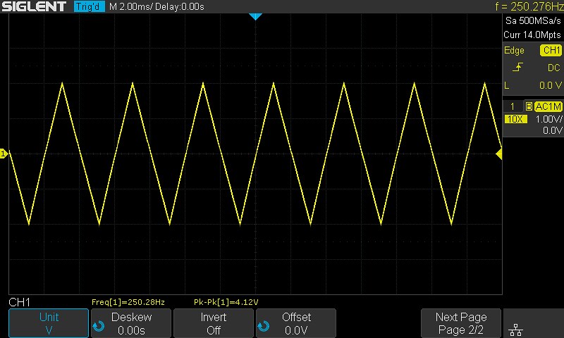
Only 250 Hz. Maybe this is the problem? When I built this circuit I know put the correct capacitor value in for oscillation pin, but I will unsolder it and measure to verify.
Is there any way to measure parasitic capacitance? Thanks very much for all the help.
Cheers! -
Quick question- in the article, is this the RC filter you are referring to?
That is the one.QuoteWhat I understand you saying, is if Cl has a large enough ESR, then Rl isn't necessary. If Cl ESR is too low, then add a small resistor in series with Cl? Or a shunt resistor as pictured?
That is right and a resistor is placed in series with the capacitor. For a standard aluminum electrolytic or tantalum capacitor, this resistor already exists in the form of the ESR.
The idea is that the output resistance of the operational amplifier combined with the shunt capacitance lowers the open loop gain below 1 before the feedback reaches 360 degrees. The ESR or series resistance adds some phase lead making this easier to accomplish and also prevents parasitic oscillation of the output stage.
It is the brute force way to accomplish this but at least in my experience, it actually provides better performance.
-
Only 250 Hz. Maybe this is the problem? When I built this circuit I know put the correct capacitor value in for oscillation pin, but I will unsolder it and measure to verify.
No no problem in this case (only a much too high frequency would bother).
On the other side:
I usually measure the frequency at the flying capacitor (with some input voltage applied)
If you are putting the scope directly at the capacitor the frequency drops somewhat due to the leakage (scope input resistor).
with best regards
Andreas
-
Time for an update-
Made some new discoveries over the weekend. I believe I have been slightly misinterpreting my measurements. I was experimenting with the LTC1043 circuit that I have seen be too low in voltage, and decided to scope the output of LTC1043. The DMM was already attached. As soon as scope probe was attached, I saw the DMM measurement drop significantly. More investigation revealed the DMM measurement dropped by 300uV when the scope probe is attached. The scope probe I'm using is 10X, 10MegaOhm input impedance. So a 10M load drops the output by 300uV. Next I realized the meter I've been using to take measurements has only 10M input impedance. So the large error I have been seeing is likely due to the DMM loading down the LTC1043 output. What I had considered to be large offset voltage of OPA227, was actually the OPA227 drawing a lower bias current than my meter! Ok I think its time to invest in a high impedance DMM!
Also some less exciting news-
Put together another LTC1043 circuit with the capacitors in anti-phase as David suggested. I immediately saw problems with this circuit, I believe I have a faulty chip or somehow damaged it. The readings were very poor. in the divide by 2 configuration I was getting readings anywhere from 80 mV to 130 mV too low.
I saw current draw on power supply go up significantly, so I decided to measure. Reading only the LTC1043 current draw, it is pulling 17.8 mA ! I think normally its supposed to pull under 1 mA. I think this may be a bad one.
I also saw the reference voltage source drop in voltage when connected to this 1043. So started probing around with the scope. Observed large switching transients on the input.
Here is the scope on the sampling capacitor, with no signal voltage applied. 800 mV transients at the switching frequency: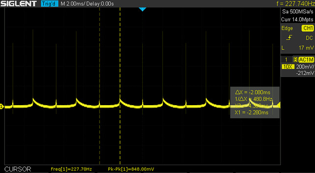
Zooming in a bit the transient looks like this: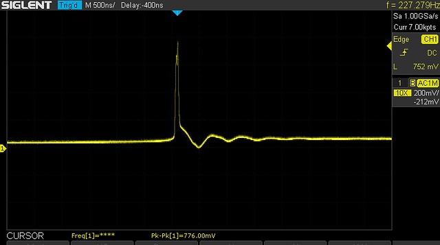
Next a voltage was applied to sampling capacitor, transients reduced in amplitude. Weird.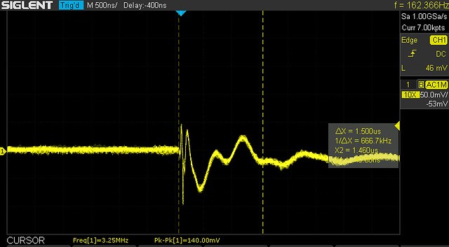
Next I measured the original LTC1043 circuit, to compare waveforms. Here is original LTC1043 sampling capacitor. 35 mV P-P. much quieter: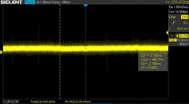
much lower noise
So the bad LTC1043 will be replaced. -
Quote
That is right and a resistor is placed in series with the capacitor. For a standard aluminum electrolytic or tantalum capacitor, this resistor already exists in the form of the ESR.
The idea is that the output resistance of the operational amplifier combined with the shunt capacitance lowers the open loop gain below 1 before the feedback reaches 360 degrees. The ESR or series resistance adds some phase lead making this easier to accomplish and also prevents parasitic oscillation of the output stage.
It is the brute force way to accomplish this but at least in my experience, it actually provides better performance.
Thanks very much for that David. I shall use this in my next circuit and report back the results! Your experience and insight is very much appreciated -
Hello Friends,
Ok I have some much better results to report. I was able to put my DMM in 10G input impedance mode, and the measurements improved significantly. Now the max error is around 90uV at 10V level, and around 50uV at 5V level. This is quite encouraging, and makes LTC1043 seem a good application as input divider for ADC. Here are the results: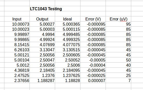
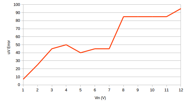
So at the 5V level Andrea has 20-25uV error, and I am getting around 50uV low. That is ok with me. I am closing in! The data doesnt seem as linear this time, almost like there are two "levels" or plateaus.
I have a couple thoughts-
LTC1043 is limited by 18V max Vdd, would this be a difficult device to make out of discrete components to allow higher input voltages?
Also, is error expected to get better or worse with larger divisor ratios? My first instinct would suggest to me that accuracy would improve with more division, but the datasheet suggests the opposite.
Cheers and thanks for help everyone! -
It is possible to build a charge pump with other, higher voltage CMOS switching chips (e.g. DG411 or similar) and a suitable clock. However other chips tend to have a higher charge injection and thus a slightly higher error is expected. There might be newer ones with comparable performance, though usually without the internal clock.
The error has three main contributions: Loading by leakage / input currents to the DMM/OP, parasitic capacitance and charge injection. So one can not expect a perfect division, but a rather stable one. The charge injection may show a nonlinear dependence on the voltage. Parasitic capacitance should be mainly proportional or constant (coupling to control lines). The loading effect would be about linear in the load.
-
I am closing in! The data doesnt seem as linear this time, almost like there are two "levels" or plateaus.
The plateaus are due to the limited resolution (quantisation error) of your DMM readings.
So you will need at least 1uV resolution or better to judge linearity.
Most instruments have one additional digit resolution if you read them out by the PC-interface.
The other way would be to use a 2nd source in series to the instrument as zero Voltmeter in 100mV range and compare both partial voltages on the LTC1043.
(from input to output and from output to gnd).
with best regards
Andreas
-
Quote
It is possible to build a charge pump with other, higher voltage CMOS switching chips (e.g. DG411 or similar) and a suitable clock. However other chips tend to have a higher charge injection and thus a slightly higher error is expected. There might be newer ones with comparable performance, though usually without the internal clock.
Aha, I see what you mean. I did some reading on charge injection. So it seems all CMOS devices have it. I read there are some mitigation strategies for countering charge injection, but that leads to complication I guess. Is that what the "Charge Balancing" function block in the LTC1043 datasheet represents? Some charge injection countermeasures?
Perhaps there is a mechanical solution. An old friend of mine had a switching capacitor military piece of equipment. It was a step up/step down converter between 12V batteries and 24V batteries. It used a multivibrator as the switching element. Maybe reed relays could be used? Or Mercury wetted relay? Maybe it is experiment time!QuoteThe error has three main contributions: Loading by leakage / input currents to the DMM/OP, parasitic capacitance and charge injection. So one can not expect a perfect division, but a rather stable one. The charge injection may show a nonlinear dependence on the voltage. Parasitic capacitance should be mainly proportional or constant (coupling to control lines). The loading effect would be about linear in the load.
I see so error terms are loading, parasitic capacitance, and charge injection. The loading can be minimized with better op amp selection. Leakage perhaps maybe improved with guarding and better construction methods. An actual pcb would probably be better than the breadboard I currently have. Regarding the parasitic capacitance, would you consider this to be mostly parasitic capacitance within the LTC1043 package, or do you think a fair percentage is coupling to other things on the board? For instance if one were to make a max effort construction of an LTC1043 divider, what improvements would you make to yield the largest gains?
This actual got me thinking a little bit on ways to improve this circuit. I will need to take some more accurate measurements to characterize the shape of the error curve precisely. If the error terms are dominated mostly be linear components, then it should be able to find a "best fit" value of resistance (very high) to connect directly between input and output. So that charge lost during switching will be supplemented by current through the resistor. Would this be a valid assumption to make? The other thought I had to improve performance, would be to utilize the other half of the LTC1043 that is not being used. Use that in a multiply configuration, but with the transfer capacitor being a very small value. Probably a few pf. This then gets added on to the output. Just some ideas I'm throwing around. I think I should do experimentation and see what happens.
Another thought I had is using a vacuum tube on the output instead of low bias current opamp. connect output of LTC1043 to vacuum tube grid, and I think then the voltage can be extracted without drawing much current. Vacuum tube voltmeter I guess.
Thankyou Kleinstein for you advice. I always enjoy your intelligent responses. Cheers -
Quote
The other way would be to use a 2nd source in series to the instrument as zero Voltmeter in 100mV range and compare both partial voltages on the LTC1043.
Thanks very much Andreas, I see what you mean by quantization error. If I have more resolution in the multimeter then I could see the "missing" parts of the line. But right now the lines is in between LSB steps of the analog converter.
(from input to output and from output to gnd).
with best regards
Andreas
I'm not sure I understand what you are suggesting for the instrumentation setup. I am trying to picture it in my mind. Is this what you had in mind? I understand it would be good to compare (Va - Vc) to (Vc - Vd), but I dont know the best method for doing that. For the "source" would it be good to use say 5V LTC6655? or maybe 10V reference through voltage divider?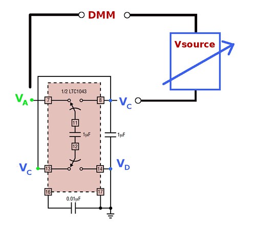
Cheers! -
Hello,
yes exactly this way.
But if you do not have a buffered input on the LTC1043 I would recommend to use a
minimum 1nF capacitor on VA to GND to filter out EMI (from cabling) which would otherwise give offsets
with best regards
Andreas
-
Another way to design a high precision charge pump is to use optically pumped switches in the form of either LDRs (light dependent transistors) or photo FETs. Optical coupling reduces charge injection significantly.
-
Another way to design a high precision charge pump is to use optically pumped switches in the form of either LDRs (light dependent transistors) or photo FETs. Optical coupling reduces charge injection significantly.
I thought LDR is light dependent resistor.
The LT1043 has quite low charge injection in the range of couple pC (p. 7).
Do you have a clue how much charge injection optically switches have? -
I love these discussions early in the morning with a cup of coffee

H11F1 claims to have no charge injection https://www.electrokit.com/uploads/productfile/41014/0900766b812cfb59.pdf
MUX36D04 http://www.ti.com/lit/ds/symlink/mux36s08.pdf
The MUX device claims ~0.5pC source-drain and ~2pC drain-source charge injection-maximum over a +-10Vpp input range (Figure 12 and 13, Vin +-10V, +-15V supply). 2pC into 1µF would equate to a 2µV charge injection error.
Also a bootstrapped LTC1043 would always stay in the region of Vcc/2 (max 18V supply, no 10Vin bootstrapped possible in this case) and therefore have minimal charge injection i presume, havent build it myself. -
H11F-series summary:
+no charge injection
-high leakage/low off resistance
-slow
-high drive current
This seems not to be a good combination for sample & hold and therefore does not impress me so much.
The MUX36 is indeed an impressive part - have to put it onto my notepad.
-
Tried to simulate the H11F1 within LTSpice as a discrete substitute for the LTC1043, file attached.
Apparently the high off-state dark current is the main problem, if i have correctly simulated the effect through the use of current sources.
By reversing the current of I2 and I4 the dark current sources eliminate each others error.
Question is if the dark current stays constant over device lifetime or if the simulation isnt correct.
Thoughts about this?
Edit: the PVA3054NS has better specs compared to the H11F1 and yields way better results in the simulation, since the leakage if much lower.
PVA3054
response time 25µs/15µs
RDSon 160R
Off-state-resistance 10GR
Off-state-leakage ~15pA typical
H11F1
response time 45µs/45µs
RDSon 200R
off-state-resistance 300MR
off-state-leakage 50nA max