-
Anything wrong with this linear PSU design? (now selecting parts)
Posted by Powermax on 01 Jan, 2017 06:33 -
I have for the longest time been working on making a nice power supply design capable of operating down to almost 0V on a single rail, capable of 3A for sure (and hopefully 5A) using 99% my own design. Just to put everything I do know about electronics to the test. I didn't crunch numbers, most of the values were guesses or very basic calculations, and messing with some values in LTspice to get a really nice stable output. I'd like more insight on how to measure the performance of the circuit please!

If I choose to use a better rail to rail op amp, and had a current source that could work down to 0V, then I would be able to acheive a perfect 0V output with a single rail supply!
If you guys think this design is sound, i'll take the time to whip up a PCB layout and order it. I purposely used a 0 to 5V pot for the voltage set so that I can use a DAC and arduino to set the voltage, and to set the current, I just need some way to convert an absolute voltage from a DAC into a current. (as close to an ideal voltage driven current sink as possible) or possibly a current DAC. I'd like 10mV resolution with an output, so at least 11 bit resolution required for 0-15V. This is a whole'nother question in it of itself.
NOTE: I uploaded a both a PDF and a .ASC (basically just txt) of my circuit, but they are slightly different versions, the spice model has more ideal components in it (to set voltage and current) and utilizes 2 complementary pairs and 2 resistors which perform both load sharing and current sense.
-
Here is a picture of the PSU design, since neither file uploaded in the original post conveniently show a picture.
-
With single transistors the current mirror (Q3,Q4) might need some emitter resistors. There a dual transistors available that can get away without them.
The Sizlaki pair output stage usually does not like to be driven from a high impedance source. So one might need something like an RC snubber at the base of Q2, or another emitter follower. There is also a chance to have it oscillating at rather high frequencies. So one might need a resistor at the emitter of Q2 to reduce the local loop gain. Also include something like parasitic inductance of the shunt - this might promote oscillation.
The LM358 is a rather slow OP and thus current limiting will respond slow - this could be a problem at a sudden short. An extra faster transistor based current limit might be needed in addition. There is currently no extra frequency compensation, it might just work with the model of the slow LM358, but usually one want's to have adjustment options. There is quite a large tolerance range for the frequency response of the LM358, especially as there are many manufacturers.
Having the current limiting OP supplied from the fixed supply also puts some demand on the OP (e.g. high slew rate, PSRR). Simple models might not includes all possible side effects.
The current source around U1 does not work all the way down to 0 V - so current limiting will not work properly at low output voltage.
One might not need the current sources around Q6 and Q7.
To test the performance in a simulation (e.g. LTspice) one can use a current source as a load at the output. AC simulation (with the current sink as AC source) gives the output impedance. Transient simulations (e.g. current jumping from 10 mA to 1 A and back) shows transient response.
For a real life circuit (e.g. on a bread-board) one could look at the transient response with switching an additional load resistor on and off. A full stability test for any load is difficult, but the simulations should show the more critical load cases.
-
I'd say that the design is rather crazy, as it uses a ton of auxiliary power supply voltages: +18V +9V +5V and some unknown -V and a ton of other auxiliary circuitry.
I also think the high side current sensing is not of the best options available.
Let me draw you something a bit different.
Most importantly - lacking any kind of protection. (negative output voltage, external voltage source - connecting for example a battery to this supply when it is powered of will certainly blow the ass out of Q1 BE junction and/or connecting any external voltage to it higher than the voltage set on this supply will definitely blow the ass out of Q2 and the opamp) -
With single transistors the current mirror (Q3,Q4) might need some emitter resistors. There a dual transistors available that can get away without them.
I figured they did make those, I'd like to try to stick with "jellybean" parts, and I have already noticed in the real world (with thermal considerations) how important those are due to annoying positive temp-co of BJTs when sinking/sourcing more than a mA or so.The Szlaki pair output stage usually does not like to be driven from a high impedance source. So one might need something like an RC snubber at the base of Q2, or another emitter follower. There is also a chance to have it oscillating at rather high frequencies. So one might need a resistor at the emitter of Q2 to reduce the local loop gain. Also include something like parasitic inductance of the shunt - this might promote oscillation.
Luckily I found this not to be a problem, but it is being driven almost directly from the op amps. The diodes essentially perform a MIN() function, so the op amp with the lowest output will "win" and take control of the feedback loop. Engenius I know
The LM358 is a rather slow OP and thus current limiting will respond slow - this could be a problem at a sudden short. An extra faster transistor based current limit might be needed in addition. There is currently no extra frequency compensation, it might just work with the model of the slow LM358, but usually one want's to have adjustment options. There is quite a large tolerance range for the frequency response of the LM358, especially as there are many manufacturers.
Having the current limiting OP supplied from the fixed supply also puts some demand on the OP (e.g. high slew rate, PSRR). Simple models might not includes all possible side effects.
I have been considering finding another better op amp. I know it's slow, it's the only op amp I have on hand (other than handfuls of LM324's) that have inputs that work down to ground. And with 10uF of output capacitance, the supply seems very stable both in simulation and in practice. Less than 3uF and you start to get some really long ringing and oscillation, and I have not found any combination of feedforward, lead lag, or even Dominant-pole compensation (mind you, I barely understand these terms, mainly I was just sticking random capacitors at random points to see if I could get a stable output. I couldn't.)
Do you know of any faster (cheap) op amps that operate down to the -Vcc rail (or preferably rail to rail entirely) that can withstand 25V? I asked this on Instructables but did not get much of a response.The current source around U1 does not work all the way down to 0 V - so current limiting will not work properly at low output voltage.
One might not need the current sources around Q6 and Q7.
These current sinks were originally in place when I used the LM324, which while it could source some considerable current, it can only sink a few tens of microamps!!! Might as well be an open-emitter output! So my idea is that the current sinks will aid the chosen op amp in sinking more current, same way current sinks / sources are used for class A amplifiers. Also it might help with crossover distortion, if that's important for some reason. Although technically unnecessary with the LM358 due to its capability to sink 5mA or so, I would like to use 10mA or more from the source biasing the Szlaki pairs to ensure they are well-driven. In practice I found my LM358 is capable of sinking over 5mA, but the output does not get quite as low as I would hope (about 1V above Vee or in my breadboard circuit, 1V above ground.) Hopefully a better (not low power) op amp will entirely eliminate the need for this.
To test the performance in a simulation (e.g. LTspice) one can use a current source as a load at the output. AC simulation (with the current sink as AC source) gives the output impedance. Transient simulations (e.g. current jumping from 10 mA to 1 A and back) shows transient response.
For a real life circuit (e.g. on a bread-board) one could look at the transient response with switching an additional load resistor on and off. A full stability test for any load is difficult, but the simulations should show the more critical load cases.
Cool! I actually did already perform a transient test almost exactly as you specified, as well as in real life with a 555 timer and a small 4V christmas lamp (which draws like 250mA and considerably more when cold) and I did get some response figures. However I have no idea what a "good" transient response is. I might test a 7808 regulator in the same way and compare the responses.
-
Seems you ignore me, but..Quote
I used the LM324, which while it could source some considerable current, it can only sink a few tens of microamps!!!
Certainly not true, you were doing something wrong. It will sink as much as it can source, enough for this application. The LM324 has different problems with its output stage (significant crossover distortion, being one of them).
Lamp is not suitable for pulse load. Use resistors as load. The lamp/bulb is nonlinear load with current changing both in time and nonlinearly with voltage.
"which draws like 250mA and considerably more when cold" - thats exactly why its useless as a test load. You need a nice square current pulses. Build yourself a pulse load, just 555 + suitable NMOS and a bunch of resistors. -
I'd say that the design is rather crazy, as it uses a ton of auxiliary power supply voltages: +18V +9V +5V and some unknown -V and a ton of other auxiliary circuitry.
The voltage rails were just arbitrarily selected, I probably should have explained that nonsense a bit I have not selected a transformer yet so those choices are volatile. Who knows, I may even choose to use a switching preregulator if I can figure out how to make a good one or find a good reg (low noise and ripple). My idea is to use a 9-0-9 transformer capable of 5 amps or more, and maybe wind a few extra turns of wire to get some random slightly more negative voltage for the op amp. Ideally, -V will end up being the same as ground. I want the output to go to 0V without the need of -V.
I also think the high side current sensing is not of the best options available.
Let me draw you something a bit different.
I do want to mirror this circuit for the negative half, so I have a dual rail lab supply (far more useful) but I figure I would first design the top half and see how good I can make it. I would be looking forward for your suggestion!Most importantly - lacking any kind of protection. (negative output voltage, external voltage source - connecting for example a battery to this supply when it is powered of will certainly blow the ass out of Q1 BE junction and/or connecting any external voltage to it higher than the voltage set on this supply will definitely blow the ass out of Q2 and the opamp)
Yikes! Thanks for reminding me. I almost forgot to add those reverse protection diodes. I'll go ahead and tack those on. I have killed a whole lot of LM317 and LM78XX regulators by adding a bunch of like 1000uF caps to the output thinking more = better. Took awhile to realize that if power is disconnected and the floating voltage on the input of the regulator was shorted, that the regulator would instantly die! So I should have known better lol
-
I am really interested as what diodes you will put there.
Meanwhile, I've drawn you some ideas. But used the negative side current sensing, as I didn't know you need high side sensing specifically.
Still, have a look how to protect the supply from any kind of external voltages properly. The 1K base resistor together with the reverse BE diode is mandatory there.
//EDIT: Now I will think a bit about your high side current sensing. I don't like the idea of placing the R2 pot like you have, as if it fails, the output current won't be limited - I like a fail safe designs, regarding potentiometers.
-
Seems you ignore me, but..
QuoteI used the LM324, which while it could source some considerable current, it can only sink a few tens of microamps!!!
Certainly not true, you were doing something wrong. It will sink as much as it can source, enough for this application. The LM324 has different problems with its output stage (significant crossover distortion, being one of them).
Not at all ignoring you! I think I quoted your entire last response with my last response.
Don't believe me, go take a look at the datasheet yourself! I was in just as much disbelief as you originally. Literally jaw dropped! Could it be possible I am looking at the wrong rating?? It's called "output current" IO and is split into 2 sections, Source and Sink. I can't imagine what else it might be referring to.
The datasheet specifies the LM324 being capable of sourcing a minimum figure of 20mA max with a typical figure of 40mA max, but sinking as little as 12 microamps (50uA typ)!!! Pathetic! The LM358 is better in this regard, but even it can only sink half the current it can source. It's singing capability is rated at 5mA over the full temperature range, with a typical optimistic figure of 20mA at 25oC I was able to sink 1mA with my LM324's, but that is well outside of it's limit and explains why my real circuit had trouble when I tried to set the current source higher than a few mA's especially when trying to get near 0V output.
My original design used LM324's, and without those current sinks, I could set the current source so I either had a supply that could provide a stable output voltage down to zero volts but with very little (less than 1A) current capability OR I had a supply which could deliver as much as 3A (maybe more if I had a power supply that could power it better) but incapable of outputting less than 4V! Or something like that, I don't remember anymore. This was mostly fixed by adding those current sources.
I could also replace the schottky diodes with PNP emitter followers but these don't work down below 0.6V above the 1(ish)V minimum output of the op amp, leading to about 1(ish)V minimum output. Then again neither to these current sources so I guess the point is kinda moot, so oh well. Whatever!
I don't suspect they are hurting anything having them there. Do you? If so please to tell me if there is a reason to remove them. As I might not even bother populating them after ordering a PCB.
[url]http://www.ti.com/lit/ds/symlink/lm2902-n.pdf]http://www.ti.com/lit/ds/symlink/lm2902-n.pdf]
[url]http://www.ti.com/lit/ds/symlink/lm2902-n.pdf
[/url]
[url]http://www.ti.com/lit/ds/symlink/lm358.pdf]http://www.ti.com/lit/ds/symlink/lm358.pdf]
[url]http://www.ti.com/lit/ds/symlink/lm358.pdf
[/url]Lamp is not suitable for pulse load. Use resistors as load. The lamp/bulb is nonlinear load with current changing both in time and nonlinearly with voltage.
"which draws like 250mA and considerably more when cold" - thats exactly why its useless as a test load. You need a nice square current pulses. Build yourself a pulse load, just 555 + suitable NMOS and a bunch of resistors.
I also used 4 82 ohm resistor to make a 1W 82 ohm resistor as a pulse load when I had the supply set to 15V output. Even used a 2W 5 ohm resistor to draw a "clean" 3A (compared to a large drill motor) and yes, I know I was WAY over pushing it at 15V, don't bother telling me! I pulsed it (plugging it in and out) for less than a second at a time and it heated up nicely too!
-
I am really interested as what diodes you will put there.
Meanwhile, I've drawn you some ideas. But used the negative side current sensing, as I didn't know you need high side sensing specifically.
Still, have a look how to protect the supply from any kind of external voltages properly. The 1K base resistor together with the reverse BE diode is mandatory there.
//EDIT: Now I will think a bit about your high side current sensing. I don't like the idea of placing the R2 pot like you have, as if it fails, the output current won't be limited - I like a fail safe designs, regarding potentiometers.
Good point. I also don't like that if one of the op amp fails, then the current source will pull the output high naturally. Imagine something happens and the op amp burns up, then the full 15-20 volts get pushed into a $$$ mobo!
 Which I guess I could argue is the reason for the current sinks as well, although that would require the sinks to sink more current than the source.
-
You say to set the output voltage and current from a DAC? Well, probably you would like also to measure the current via an ADC. That would require a completely different approach to what you have currently.
You will need to sense the current from the high and low rails, convert it down to a voltage against the ground - most probably using an instrumentation amp. (AD620 seems to go cheap on Aliexpress, by the way)
I'd suggest to use completely different circuit topology, as this one does not give much chances with the current sense/set problem by a DAC/ADC respectively.QuoteDon't believe me, go take a look at the datasheet yourself! I was in just as much disbelief as you originally. Literally jaw dropped!
Could it be possible I am looking at the wrong rating?? It's called "output current" IO and is split into 2 sections, Source and Sink. I can't imagine what else it might be referring to.
No, I do not believe you, so shouldn't you believe the Texas Instruments datasheets. Those fucks shall clean their mess up, as the sink current is not uA, but 10 to 20mA. The uA is for the second row of values. Check with datasheets from different manufacturers.
The key here is the note about Vo voltage: 1V --> up to 20mA sink, 10mA typical. BUT, at Vo 200mV, the sink current will be tens uA. Vo is the output voltage against the V- supply pin and yes, the values does make sense a lot, if someone didn't mess the units up.QuoteGood point. I also don't like that if one of the op amp fails, then the current source will pull the output high naturally. Imagine something happens and the op amp burns up, then the full 15-20 volts get pushed into a $$$ mobo!
Which I guess I could argue is the reason for the current sinks as well, although that would require the sinks to sink more current than the source.
You shall design the circuit in such way, the opamp cannot burn by improper handling of the power supply. If you assume the opamp goes bad by itself, you can then expect even the output transistor to burn - in both cases, nothing you can do with it. However, the potentiometer fail can be caught up in the design.
You can also design in another opamp/comparator to sense the output voltage independently and compare against the setpoint: If it differ too much for a given time, you can for example trigger an SCR to short the supply input leads and blow a fuse. -
Quote
You say to set the output voltage and current from a DAC? Well, probably you would like also to measure the current via an ADC. That would require a completely different approach to what you have currently.
You will need to sense the current from the high and low rails, convert it down to a voltage against the ground - most probably using an instrumentation amp. (AD620 seems to go cheap on Aliexpress, by the way)
I'd suggest to use completely different circuit topology, as this one does not give much chances with the current sense/set problem by a DAC/ADC respectively.
My very original design used a craptacular differential amplifier (4 resistors and an op amp) converting high side voltage differential from the shunt into a voltage referenced to ground, which was trivial to feed into a error amp (comparator) which would have also trivial to feed into an ADC. But the loop was too big, too many components in the loop (crappy differential amp, an error amp, a few diodes and transistors, output pass transistor..) and the design was not stable at all. A instrumentation amp might be better suited but I still don't want too many active components with additional propagation delays decreasing phase margin.
That's what led to this design, in search for a simpler / less naive solution. To implement a ADC to measure current, I would probably just implement a special purpose current measuring chip across the same shunt and feed that to a cheap I2C ADC. This design is mostly a first attempt, and I will make modifications down the road to turn it into an arduino controlled dual rail supply. But I just want something that works right now, and is simple to power.QuoteThe key here is the note about Vo voltage: 1V --> up to 20mA sink, 10mA typical. BUT, at Vo 200mV, the sink current will be tens uA. Vo is the output voltage against the V- supply pin and yes, the values does make sense a lot, if someone didn't mess the units up.
Ahh, that does make a lot more sense. Basically the less current I sink, the lower the output voltage of the op amp can become, down to as little as 100mV with essentially no current draw. This holds true with my experimentation especially regarding the LM358. Output goes down to essentially the negative rail but as soon as I connect any load from Vcc then the minimum output becomes like 0.6 to 1V. I end up with a tradeoff between the maximum output current of my power supply design and the minimum reachable voltage with a single-ended input. The ON-semi datasheet holds up with your claims, but the parts I have I believe are TI parts. Is there any way I can acheive this 100mV or 200mV output voltage from the op amp while sinking 10mA??? If so that'd be wonderful! -
The LM324 is the quad version of the LM358. So the OPs properties are essentially the same, within the usual variations between samples and sources.
A slightly better OP could be OPAx170 and OPAx171. For the sinking they give 1 mA at 70 mV. So 5 mA at 200 mV might work. For a mains powered supply you should not need to be so scary about an extra 600 mV of drop out.
Unless you have really special needs (e.g. 4 quadrant operation), I would build a dual supply as two fully separate supplies, that can optionally be connected in series. This is how most (if not all) of the commercial dual supplies work. It makes things much easier and also more flexible and easier to develop and test.
For a digital controlled supply, I would prefer the type of circuit HP was/is using: with a floating supply for the regulator, with an extra transformer tap or transformer. Here you have the signals for current and voltage control together and the auxiliary supply can also power the µc / display part.
One problem with the circuit Yansi had drawn and to a slightly lesser part in the circuit from the beginning is, that current limiting is slow, as it needs the OP slew down all the way to the new voltage (which would be near GND in case of a short). This transition from CV mode to CC mode is one thing one should simulate too. -
The LM324 is the quad version of the LM358. So the OPs properties are essentially the same, within the usual variations between samples and sources.
Ehh, I was afraid someone would say that. I knew they were very simalar but not the same, I thought the 356 was supposed to be better/newer.A slightly better OP could be OPAx170 and OPAx171. For the sinking they give 1 mA at 70 mV. So 5 mA at 200 mV might work. For a mains powered supply you should not need to be so scary about an extra 600 mV of drop out.
Unless you have really special needs (e.g. 4 quadrant operation), I would build a dual supply as two fully separate supplies, that can optionally be connected in series. This is how most (if not all) of the commercial dual supplies work. It makes things much easier and also more flexible and easier to develop and test.
I guess you're right. I might as well move my current shunt to the low side, although I don't like it that way for some reason. It bothers me that the negative of the power supply is not the same as the output negitive, IDK why. Guess I'm OCD like that!
Those op amps look perfect, but what is the slew rate of them? 0.4V/uS? (guesstimating from the graphs) Does not seem much faster than the LM356 at 0.5V/uS.For a digital controlled supply, I would prefer the type of circuit HP was/is using: with a floating supply for the regulator, with an extra transformer tap or transformer. Here you have the signals for current and voltage control together and the auxiliary supply can also power the µc / display part.
One problem with the circuit Yansi had drawn and to a slightly lesser part in the circuit from the beginning is, that current limiting is slow, as it needs the OP slew down all the way to the new voltage (which would be near GND in case of a short). This transition from CV mode to CC mode is one thing one should simulate too.
The same problem exists with my current design, I did realize that, and I was afraid that might be an issue. Especially with these slow LM358s. To fix that, I just tacked on a little BJT with the collector to the output, emitter to the inverting input of the current amplifier, and a few diodes in series with the base, connected to the output of the current error amp. This ensures the voltage on the output of this error amp is clamped (via creating a secondary feedback loop) to a few Vd's above the voltage output. This way the op amp does not need to slew very far to take over. Hopefully leakage current through the BJTs will not cause too big an error on the voltage output.
I posted a picture of this new circuit below. I will gladly repost the full .ASC file if you would like to analyze it further!
-
if you are interested, here is a circuit based around HP way of having 2 supplys, one for the supply itself and one for the op amps. it gives good performance and was basically designed by Kleinstein:
-
The last schematic I posted (with a small mod to keep the voltage on the current limiting OP not too high) had a wiring mistake, the BJT collector goes to the output, and I replaced the diodes with an LED so it would glow when current-limiting. (although it's brightness depends on how "much" it is CC'ing.)
-
if you are interested, here is a circuit based around HP way of having 2 supplys, one for the supply itself and one for the op amps. it gives good performance and was basically designed by Kleinstein:
WOW, that circuit looks super difficult. Can I have the spice circuit model? I want to clean it up a little and try and figure out what it's doing. I the output is "ground" which is strange, I like that the voltage inputs to the op amp effectively track the output, that's smart so it avoids needing medium/high voltage op amps. -
Replace TL072 with LT1017 or something, its just for the cc or cv led indicators so not important. Replace the pass transistor (2SC5200) with any fast high power npn from ltspice libary.if you are interested, here is a circuit based around HP way of having 2 supplys, one for the supply itself and one for the op amps. it gives good performance and was basically designed by Kleinstein:
WOW, that circuit looks super difficult. Can I have the spice circuit model? I want to clean it up a little and try and figure out what it's doing. I the output is "ground" which is strange, I like that the voltage inputs to the op amp effectively track the output, that's smart so it avoids needing medium/high voltage op amps.
-
Looking at it more carefully, it appears that he did a few things the same way I did. Using diodes as a MIN function the same way I did, and (now) using a transistor to ensure the output of the op amp does not go too high when not controlling the feedback loop. There is a lot of compensation components in place, pF capacitors everywhere, something my supply did not require (likely due to a slow op amp)
One problem I do have is that the voltage control is not referenced to ground, so controlling it digitally with a DAC would require a another supply referenced to the output if I am not mistaken, and the digital control of it would need to be galvanically isolated from an arduino referenced to ground (whatever that is, I'm not even sure!)
SO my question now is how to I figure out what value of compensation components I should use to stabilize the output if it was not stable itself? -
That is a great design and reminiscent of the Tektronix PS501 or PS503.
358/324 operational amplifiers do have problems sinking current below 0.6 volts because of their emitter follower output stage. Modern single supply or rail-to-rail output operational amplifiers do better. For instance the LT1013/LT1014 are improved replacements for the 358/324 and can sink current all the way to ground. The Tektronix PS501 and PS503 solved this problem by using a low voltage negative bias supply for the operational amplifiers which were just 301As or 741s.
I like your solution even if it is not perfect. Using a Darlington output stage with its additional Vbe drop would help.
-
I changed out the LT1007 / 1037 ( even though it isn't the ideal choice in this design) and got discusting parsitic oscillation, how am I supposed to stop this? How do I go about frequency compansation?
-
I changed out the LT1007 / 1037 ( even though it isn't the ideal choice in this design) and got discusting parsitic oscillation, how am I supposed to stop this? How do I go about frequency compansation?
It's a very big topic and the most complicated about designing a PSU.
http://www.linear.com/solutions/1831
http://www.allaboutcircuits.com/technical-articles/negative-feedback-part-1-general-structure-and-essential-concepts/
http://www.allaboutcircuits.com/technical-articles/negative-feedback-part-3-improving-noise-linearity-and-impedance/
http://www.allaboutcircuits.com/technical-articles/negative-feedback-part-4-introduction-to-stability/
http://www.allaboutcircuits.com/technical-articles/negative-feedback-part-5-gain-margin-and-phase-margin/
http://www.allaboutcircuits.com/technical-articles/negative-feedback-part-6-new-and-improved-stability-analysis/
http://www.allaboutcircuits.com/technical-articles/negative-feedback-part-7-frequency-dependent-feedback/
http://www.allaboutcircuits.com/technical-articles/negative-feedback-part-9-breaking-the-loop/
http://www.allaboutcircuits.com/technical-articles/negative-feedback-part-10-stability-in-the-time-domain/ -
Adjusting the frequency compensation is one of the more difficult parts. You are very lucky if it works just with using an OP the is just slow enough.
The LT1037 in the circuit shown by ZeTeX is not the obvious choice. Depending on the supply it is more like the TLC272 or LT1013 if high precision is wanted. The large number of capacitors for compensation is in part from keeping several optional ones and in optimizing the CV-CC transition very much. The larger number of parts to adjust also allows stability with any possible passive load, not just a simple resistors.
Similar the transistor Q3 is not absolutely needed - it still works without it, just with slower CV-CC transition, but still better than with the other single supply circuit from the beginning. This extra transistor is usually not found in similar circuits. Otherwise many of the cheap chinese supply use a similar circuit type (leaving out a few more caps and more like an LM358 class OP). Also transformer tap switching is usually added with 2 relays.
The circuit needs a separate supply for the OPs part and this supply would also supply the controlling µC. Due to the separate supply the circuit uses a different concept than the original circuit. The diodes are used to get the min value for the output current, as opposed to the output voltage in the other circuits at the start of this thread. -
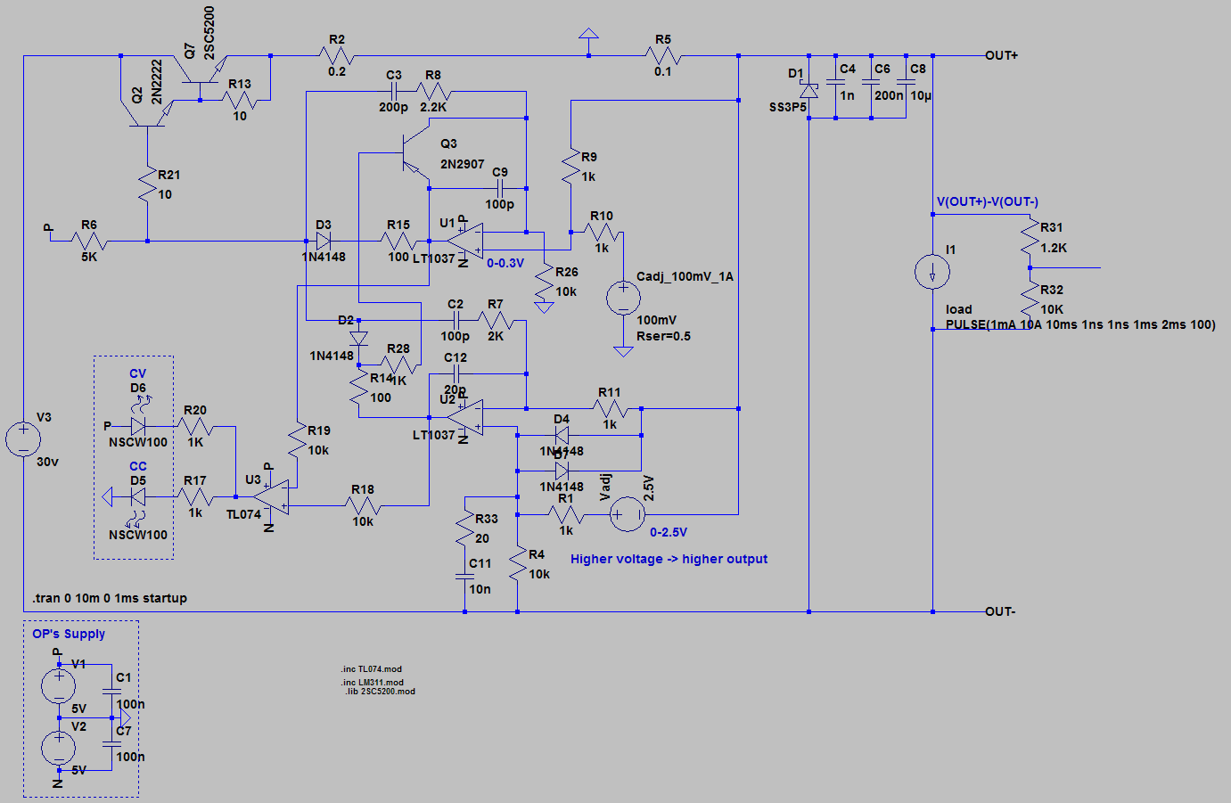
I changed out the LT1007 / 1037 ( even though it isn't the ideal choice in this design) and got discusting parsitic oscillation, how am I supposed to stop this? How do I go about frequency compansation?
Do not use the LT1037; it is decompensated for use at gains of 5 or greater. While it is possible to externally compensate it for lower loop gain with a series RC network between the inputs, this will result in higher noise than using an LT1007 because you have to raise its noise gain to make it stable and it adds complication.
Add type 3 frequency compensation to each operational amplifier. All of the parts may not be needed but I usually include space in the layout for them. This includes the standard capacitor and series resistor-capacitor networks from the operational amplifier outputs to their inverting inputs and similar lead networks around R2 and R11. R2 should be fixed and the current from the current sink made adjustable.
If the output capacitor ESR is too low, then that will make compensation more difficult. At least to start, remove C1 and C4; they will not do any good for decoupling of a remote load anyway. An appropriate value for RF decoupling can be added later although I have never found it to be necessary.
U2 is not going to work correctly at low and high output voltages because its common mode input range will be exceeded. The mode can be detected by the current flowing into the outputs of U1.1 and U1.2.
-
Quote
Do not use the LT1037; it is decompensated for use at gains of 5 or greater. While it is possible to externally compensate it for lower loop gain with a series RC network between the inputs, this will result in higher noise than using an LT1007 because you have to raise its noise gain to make it stable and it adds complication.
I won't! I knew it wouldn't be stable but I wanted to see if adding the compensation capacitors that were in Kleinstein's design would work. It didn't. The LT1007 was easier to stabilize but with my current design the LT1007 would require a negative auxiliary, due to common mode input and output limitations.
I think I am going to change around my design radically, to move the current shunt to the low side and enable the use of a wider range of op amps. I have a whole bunch of op amps, mostly LM324's, but some really nice LT parts as well. Almost none of them are rail to rail input/output, so I prefer my design to use junk I already have: (bolded ones are ones I may consider using.)
LM324; // slow, crossover distortion issues, but I have a bunch
LM224; // ditto, but in weird thicc package
LM386; // slow, crossover distortion issues
LM741; // ancient relics of the past, I literally have handfuls of them!
UA1458TC // ancient relics of the past, I have a bunch of these!
LM318H; // it's in a fancy metal case
TL072CP; // JFET inputs, limited output current and the output can't go below the noninverting input.
TL2072AC; // ditto.
OP37; // These things aren't even that fast and can't work at unity gain.
OP27; // ditto
LT1007; low noise, moderatly fast
LT1167;
LT1191;
LT1363; CRAZY fast, 1000V/uS!!! Maybe too fast... Not even going to try to calm it down and stabilize it!
LT1360; fast!! 800V/uS!!!
LT1112;QuoteThat is a great design and reminiscent of the Tektronix PS501 or PS503.
Thanks! I took a look at the manual for the PS501 and I see what you mean.