-
Inductive Cell Balancing - How this analog OP Amp circuit work?
Posted by hitech95 on 24 Jun, 2020 20:08 -
Hi,
I've seen a new chip (ETA3000) that is an active balance IC. It is able to push/pull energy from/to adjacent cells.
Now after some research I've discovered that it's similat to a Synk DC DC Buck layout.
Curious on how it work I've then started my more in deep research.
I've seen the following Application Note: https://www.nxp.com/docs/en/application-note/AN4428.pdf
And to mee it seems quite straightforward.
But I actually don't understand the two formulas to calculate the hi/low side timings but for that there is time, if someone explain to how it works , the values don't match between the description and the calculations
  .
.
After some more research I've found the following project, he is doing the same I was thinking (Why don't use a DC buck IC?):
http://www.afdhalatifftan.com/2017/06/low-cost-active-battery-balancer.html
But after scratching my head I still don't understand how it's working. ('ve got the general concept but that OP AMP configuration looks strange to me, more I try to figure out how it works less make sense to me)
For reference: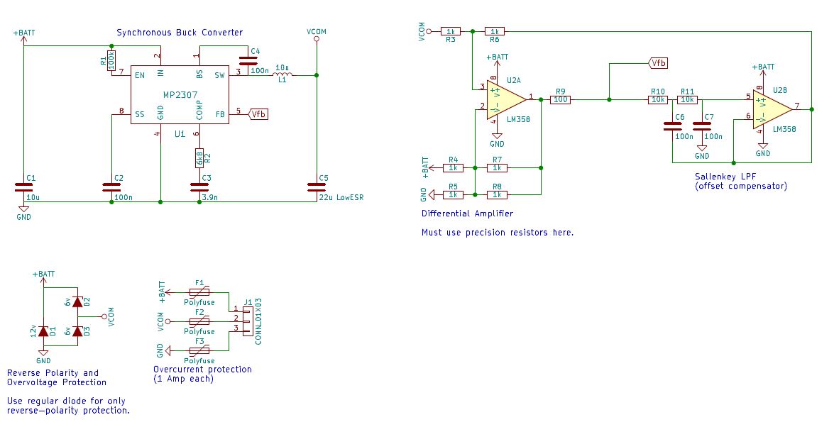
This concept is quite interesting, but are those chips able to handle the reverse inductor current? In fact when your lower side cell have more energy than the hi cell the current flow in reverse.
How can I find this value in the Datasheet of the IC? I've found nothing.
Regards, hitech95
-
No one?

I'm more a digital guy so this is a bit off my comfort zone. But I was not expecting that a "differential op amp" (It has marked as that in the schematic but I can't understand that topology ) could be that difficult to understand.
-
Don't see how it can work. AFAICS it can only transfer charge from the top battery to the lower but not the other way round.
-
Active balancing makes no sense in 99.9% of cases in general anyway, what are you trying to achieve? Big (think 70kWh+) automotive packs have passive cell balance current in the order of 10mA per brick for reference.
-
Some synchronous buck converters can sink and source current, so it's possible this could work.
-
I think the best way to do cell balancing is with a flyback on each cell......if a cell goes higher in voltage....then draw current out of it with the flyback and shovel the current back into the whole series stack...like the LT8854 does.
-
I think the best way to do cell balancing is with a flyback on each cell......if a cell goes higher in voltage....then draw current out of it with the flyback and shovel the current back into the whole series stack...like the LT8854 does.
that's what a synchronous buck does, look at the schematic of a buck from output to input, it is the same as a boost -
Yea, the general idea of Inductive balancing is in my head, the issue for me is that op amp configuration, how does it works? (And yes it works, I simulated is and its fine)
But I cannot understand how! It should be an differential amplifier, the feedback resistors are 1/2 the input one so the gain should be 1/2.
But again R6 is 1kOhm is it should be equal to Rf to form a differential amplifier. that seems to be used to have a voltage offset (The one to keep the DC DC converter in equilibrium) when the two cells have the same potential.
-
Some synchronous buck converters can sink and source current, so it's possible this could work.
Yea, but how is that parameter called, I've searched on multiple datasheets some reference about the reverse inductor current but I've found nothing.
The only thing I've found is this AN:
https://www.ti.com/lit/an/slua962/slua962.pdf?ts=1593603126854&ref_url=https%253A%252F%252Fwww.google.com%252F -
that's what a synchronous buck does, look at the schematic of a buck from output to input, it is the same as a boost
A flyback can have windings for an entire stack and deliver energy in a single cycle, a stack of charge equalisers with inductors will have increasing switching losses the further the energy has to get carried. -
Quote
that's what a synchronous buck does, look at the schematic of a buck from output to input, it is the same as a boost
Yes, but For a series stack of cells, its best to use a flyback SMPS on each cell, because the flyback outputs are isolated, and they can all be dumped back into the entire stack. -
Has anybody found a western equivalent for this IC? It seems like it could potentially be a much simpler-to-implement active battery balancing system than chips like the LTC3300 which is a full-blown BMS.
-
Without getting into the generic debate on whether active cell balancing is necessary or not for any individual applications... I'll just comment on the original question.
You will find a number of bi-directional buck converter ICs out there, I'll maybe dig for some part numbers later, but essentially, any synchronous buck converter IC, (unless already spec'd for working bi-directionally), which does NOT use any current mode control, current feedback or anything to do with an inductor current it'll always assume to be positive *should* work.
Far those op-amps, the first one is still a differential amplifier, it just has a gain of 1/2 for the Vbat input, so the resulting diff-amp is calculating the error between Vcom and a theoretical Vbat/2 and feeding that as an error signal to the buck... I'm assuming that Vbat is made up of two series cells and Vcom is the voltage in the middle, the ideal voltage on that cell would therefore be Vbat/2... a long winded way of saying that each cell will have the same voltage.
The trick to analysing that circuit is to work out two conditions, one for DC and one for transients (AC). At DC the gain of the LPF is +1 and so you can disregard the second opamp and mentally connect Vfb to the right hand side of R6. For transients and AC you can assume that the gain of the LPF is very small and again disregard the second opamp and mentally connect the RHS of R6 to 'ground' this time. So the result (I think.. until I sit down and do some maths) is a higher gain at DC than for transients... which makes sense for control stability etc.
I'm assuming that the idea behind that circuit is to balance any number of series connected by forcing any single cell to be half the voltage of sum of its voltage and that of the one above it. Which in reality for more than 2 cells sounds like a recipe for chaos and fire... in theory it sounds wonderfully simple though. -
the ETA3000 just has a 50% duty cycle, and only runs if the midrail differs a few mV from half of the bottom and top rail. simple and effective.
the maximum current to balance is somewhat limited. need to find a trick to boost that.