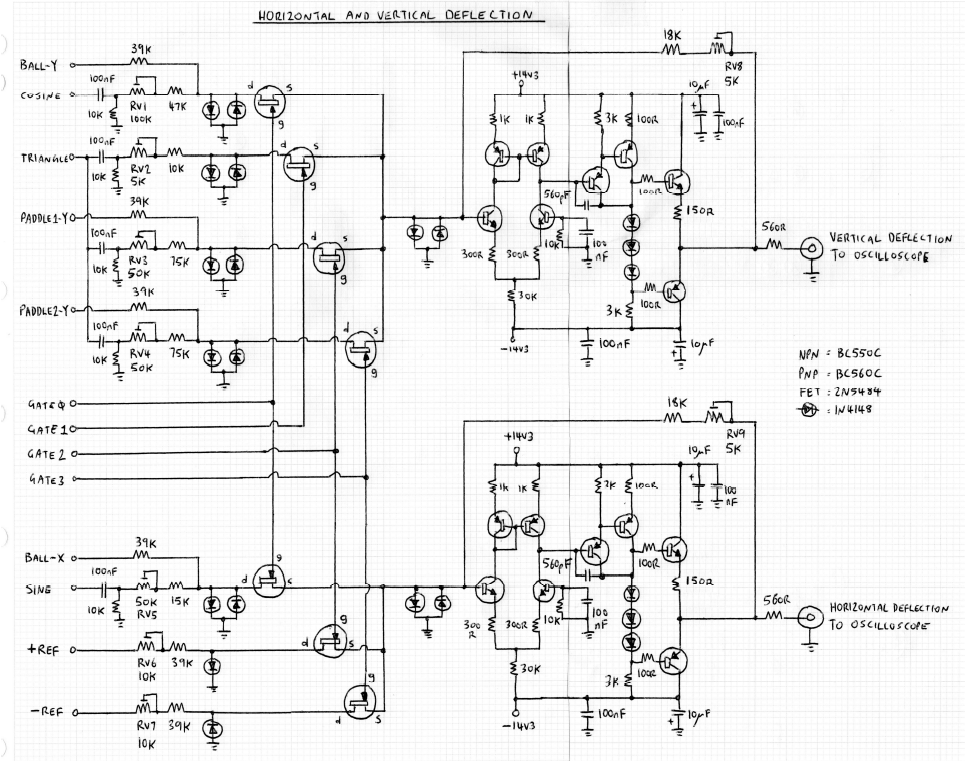
Another schematic diagram hot off the press. All that is left to draw now is the multiplexer amplifier pair that finally combines everything together for the vertical and horizontal deflection signals. Oh, that and the +/-14.3V power supply, which I haven't actually built yet as at the moment the unit is being powered from my bench supply. The power supply will be a very simple affair: 15V Zener diodes biasing series pass emitter-followers.

Finally, the semiconductor tally (this includes the as yet un-built power supply):
BJTs - 184
JFETs - 11
Diodes (Si) - 130
Diodes (Zener) - 5
Finally, the semiconductor tally (this includes the as yet un-built power supply):
BJTs - 184
JFETs - 11
Diodes (Si) - 130
Diodes (Zener) - 5
I can't seem to quickly come up with a more exciting/amazing project, to make with those 330 discrete semiconductors.

The final schematic diagrams. Phew!

I can't seem to quickly come up with a more exciting/amazing project, to make with those 330 discrete semiconductors.
Well I've now posted up the full schematic, so you can start compiling your BOM. If you want I can post a full resolution photo for layout assistance
I have one minor addition for the analog computer player which might not be to difficult to incorporate. Instead of making the paddle track instantly the balls vertical location, add an inductor/cap/adjustable resistor (the inductor is to give the computer player a life-like wave motion instead of just speed limitation) delay to fudge up the positioning of it's response giving the player a chance to win when the ball gets really fast. Having a difficulty skill setting for the analog computer by setting how fast and accurate it's paddle responds...
Once again,  an amazing work.
I did have almost that exact idea - to put an RC time constant between "Ball-Y" and the machine-driven paddle-Y. The idea is that the speed of the ball would eventually become too fast for the machine-driven paddle to catch it; if you could keep up for that long you'd invariably win. That would require buffering the RC after "Ball-Y" from the respective paddle-Y input though, as the paddle-Y inputs are 10k||39k; a value of R for a practical value of C would otherwise attenuate the signal. Another idea was to have selectable paddle sizes and an additional pair of window comparators in the "Ball-Paddle collision detection" circuit so that the ball could be made to deflect at a different angle if it hits the outer edges of a paddle rather than the middle. The scope for building upon the basic concept is endless, but one has to draw the line somewhere!
Nice. Anyone who wants to draw the schematics in KiCad? Otherwise I could try it, good learning project, because I'm switching from Eagle. The hierarchical feature (missing in Eagle before V7) might be useful for this complexity.
There is not even any opamps in there!
I count 9 op-amps!
Well okay there are discrete opamp cirucits but i meant that no opamp chips are in the design. I know if i ever went to do something like this it would end up a heap of quad opamps stringed together with passives. But that would not look as impressive for sure.
If you ever put this piece of art in to a case make sure the case has a window to let you see its guts. Perhaps also add in a few LEDs on interesting signals (Like ball movement directions and sound)
I can't seem to quickly come up with a more exciting/amazing project, to make with those 330 discrete semiconductors.
Well I've now posted up the full schematic, so you can start compiling your BOM. If you want I can post a full resolution photo for layout assistance
If enthusiasts end up laying this out as an "open source" type of project, onto a PCB. I imagine it will be a highly tempting fun project, for many on this forum.
The parts cost is probably low, with no hard to get components.
But as regards that style of construction, although I admire your work and relative neatness in making it that way. I would probably find it too frustrating, to attempt to make it that way.
If you weren't joking, full/high resolution pictures would be very nice to look at anyway. Even if that method of construction is not really my cup of tea. But I'd seriously consider it for small, very high frequency/performance projects, as a possible option.
E.g. When making a small/simple, but super fast transition avalanche pulse generator.
Don't sneeze or one of the several trimmers might get knocked off cal!

Seriously though, this thing is amazing. That seems like a lot of work to get running. Kudos to you!
Nice. Anyone who wants to draw the schematics in KiCad? Otherwise I could try it, good learning project, because I'm switching from Eagle. The hierarchical feature (missing in Eagle before V7) might be useful for this complexity.
I was actually thinking about laying this out in DipTrace as a fun project. I'd of course open source the boards, that is assuming GK doesn't mind.

Edit: Thinking about this some more, it could be converted to a PCB pretty easily, but the transistors would need to be changed to something a bit more easily available. Looking at the ratings of the BC550, I imagine they could be swapped out with 2N3904's (or MMBT3904's for a SMD kit) without issue, yeah?
Edit 2: Maybe not, the BC550 has an hFE of 110-800 while the 3904 is 100-300. Hmm, no matter, I'm sure I could find a cheaper, well stocked replacement.
Edit 3: Hmm, BC850/860C would do nicely for a SMT design. The fT is a bit slower, but I think that would be alright here. Around $0.06 in quantity.
I would totally build one of these if there was a reasonably priced board available. Because if there's one thing I need it's more projects
Hmm, BC550C/BC560C are readily available from all the major distributors:
http://www.digikey.com.au/products/en?keywords=bc550c
http://www.digikey.com.au/products/en?keywords=bc560c
The SMD (sot-23) versions are BC850C and BC860C, also readily available:
http://www.digikey.com.au/products/en?keywords=bc850c
http://www.digikey.com.au/products/en?keywords=bc860c
Note that if doing an all-SMD copy the power dissipation of many parts will have to be checked.
The to-92 2N5484 FET is obsolete, but the sot-23 equivalent (MMBF5484CT) is active and readily available:
http://www.digikey.com.au/product-detail/en/fairchild-on-semiconductor/MMBF5484/MMBF5484CT-ND/3042817
Any JFET substitute needs to have max. Vgs off spec comfortably under -10V and preferably not an order of magnitude greater junction capacitances than the 2N5484. The latter in particular needs to be watched in this application because the JFET capacitance is hanging on the sensitive virtual earth node of discrete op-amps. Some ultra/very low Rds-on "switching"-type JFET types can have very high junction capacitances, so be careful.
I think it would be great for anyone would commit to an open-source duplication of the design; just give credit to the origin!
Yeah, I saw the BC550C on Digi-Key, but it only said 800 in stock ~30 minutes ago, and they're $0.3/ea in small quantities. Whereas the BC850's are $0.1 and have 50k+ in stock.
My thought would be to do a mixed technology board. Use SMT transistors and TH caps, diodes, etc.
Perhaps release it as a kit, with the SMD stuff pre-soldered and let them stuff all the TH stuff by hand?
Why have the SMT parts already soldered? That always bugs me, just let me build the whole kit. If someone is going to have a use for something as esoteric as analog oscilloscope Pong, they ought to be able to hand solder SMT parts. We're not talking 672 pin BGAs here.
Amazing work, GK! That's a lot of point-to-point-to-point-to-point-...
Tim, looking forward to seeing your kit of it. Perhaps have the option to assemble everything, including SMT parts.
Any JFET substitute needs to have max. Vgs-off spec comfortably under -10V and preferably not an order of magnitude greater junction capacitance than the 2N5484. The latter in particular needs to be watched in this application because the JFET capacitance is hanging on the sensitive virtual earth node of discrete op-amps. Some ultra/very low Rds-on "switching" JFET types can have very high junction capacitances, so be careful.
I think it should be all through-hole, looks more authentic
Would this JFET work?
http://www.digikey.de/short/32rhf3
I think it should be all through-hole, looks more authentic
+1 , and also sort of 70s style pcb layout.
I think it should be all through-hole, looks more authentic
+1 , and also sort of 70s style pcb layout.
Right, with these squiggly traces:

But with two layers I could do it without bodge wires
Yes, squiggly traces are imperative for the vintage look.
Well you sure wouldn't want to make one of those in Altium. Those curve trace tools it has are better at frustrating you than actual drawing the right kind of curvy trace that you want.
Any JFET substitute needs to have max. Vgs-off spec comfortably under -10V and preferably not an order of magnitude greater junction capacitance than the 2N5484. The latter in particular needs to be watched in this application because the JFET capacitance is hanging on the sensitive virtual earth node of discrete op-amps. Some ultra/very low Rds-on "switching" JFET types can have very high junction capacitances, so be careful.
I think it should be all through-hole, looks more authentic Would this JFET work? http://www.digikey.de/short/32rhf3
That JFET looks fine. The transconductance is about the same as the '5484. Vgs-off max. is higher but still within limits. Rds-on might even be lower than the '5484.
Just a quick note on 'scope compatibility for anyone getting excited over building the design. Your analogue 'scope needs to have a suitable Z "blanking" or "intensity modulation" input.
The Z-input waveform is a 1200Hz squarewave which cuts the 'scope's CRT beam off when high. This squarewave is phased so that switching of the analog multiplexer occurs in the middle of the high period. Blanking the beam ensures that switching glitches/artifacts aren't visible on the display and nor is the trace as it jumps from one drawn object (which goes: ball, court divider, paddle1, paddle2, ball, court divider, ........ and so on) to the next. The blanking waveform generated is about 14V peak, which is adequate for total beam cut-off for most oscilloscope Z-inputs.
From one of my LTspice simulations of the design, here is what the typical X,Y,Z waveforms which scribe the display look like:

Well you sure wouldn't want to make one of those in Altium. Those curve trace tools it has are better at frustrating you than actual drawing the right kind of curvy trace that you want.
`
Arrrrg, now you tell me, after a decade ago I went through hell making nice PCBs with swiggly traces in Protel99, and cleaning up after all it's bugs...
Just a quick note on 'scope compatibility for anyone getting excited over building the design. Your analogue 'scope needs to have a suitable Z "blanking" or "intensity modulation" input.
The Z-input waveform is a 1200Hz square wave which cuts the 'scope's CRT beam off when high. This square wave is phased so that switching of the analog multiplexer occurs in the middle of the high period. Blanking the beam ensures that switching glitches/artifacts aren't visible on the display and nor is the trace as it jumps from one drawn object (which goes ball,court divider,paddle1,paddle2,ball, court divider,........ and so on) to the next. The blanking waveform generated is about 14V peak, which is adequate for total beam cut-off for most oscilloscope Z-inputs.
From one of my LTspice simulations of the design, here is what the typical X,Y,Z waveforms which scribe the display look like:
For those making a public source design, I would recommend making a second inverted 'Z' in case their scope or x/y display blanks on a low Z signal input instead of a high.