-
Back to back N-Channel mosfets, does source need a pulldown?
Posted by NaDobraNich on 29 Mar, 2024 21:34 -
I have a device on the left with a 3V3 pullup. On the right is an external connector that could have ground, 3-18V.
My plan was to enable the gate when I knew it was safe to do so.
1. What is the S1/S2 voltage when D2 is open? I think it'll be some number more than 0V but a little less than 3V3 and this is all because of leakage, so no real current.\
2. I also assume that means I can not use 3V3 on the gate, but would need 5V+
3. Is it OK that S1/S2 is floating? Is that 1M resistor helping? Can I remove it? I kind of figure with D2 open, that S1/S2 could be a lot of erratic voltages so I was going to determinism. I'm pretty sure 1M won't mess with my signal, but a JTAG signal so I would need to test that.
-
No need of pulldown there.
It's much simpler to use P-channel fets.
You can sample the voltage after the first mosfet, knowing there's a diode in between, and turn the fets on when a safe voltage is detected.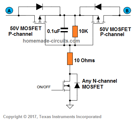
-
It's the gates which may need pull-up/down resistors.
The circuit doesn't make much sense on it's own, even with the brief description. What sort of signal is it switching? -
No need of pulldown there.
It's much simpler to use P-channel fets.
You can sample the voltage after the first mosfet, knowing there's a diode in between, and turn the fets on when a safe voltage is detected.
Yea, I saw a TI document that showed that. For their bidirectional power switching. Unfortunately, I'm using SOT363 sized dual mosfets because I'm very space constrained, and then cost constrained. So I'm not sure I can afford size withe discretes or cost with an integrated part. But I would love an integrated part there.
I think you're saying I can protect A or B by using an ADC or comparator or whatever between A and B somewhere above the NPN in order to see if either A is bad for B or vs. I like that. But it doesn't apply here. I need to protect all the time unless there is a gate voltage, if there is a gate voltage, I know it's already safe.
I'm not sure that is easier than a dual NPN. The only issue I see with mine is that I need a larger gate voltage than my signal, which is fine. I can get 9-12V there very easily. My concern was thinking that S1/S2 would be floating. But it isn't. It's subject to leakage is all, small, but enough to drive the voltage too high for a 3V3 gate.
So... If using my circuit. If I had a pull down, it would be more likely to trigger gates with a 3V3 wouldn't it? Because G to S1/S2 would always be over Vth? Same if the right side was grounded no? But without a pulldown, and without right side to ground, S/1S2 would be 3V3, and not work.... I'm guessing.It's the gates which may need pull-up/down resistors.
The circuit doesn't make much sense on it's own, even with the brief description. What sort of signal is it switching?
Yea, there is a 1K gate protection resistor, and a 47K pull down for bias. It's for a JTAG data signal, so I'm trying to not molest it too much. I am putting in a spot for a cap to ground and a small value resistor, IDK if I'll need them or the values. And I'm not sure if I'll have to slow JTAG down. It's for programming only but in circuit I can't guarantee what signals the external connector will have.
-
Using N-channels on the high side means your gate voltage to turn on the mosfets will have to be Vth+ above the highest voltage that will be flowing through. So I agree that P-channel is the way to go here.
And for some reason I see this with the drains connected together. It doesn't matter if the drains float.
-
What about using a single BJT?
A BJT can work in reverse, given certain limitations: the hFE is much lower, typically only about 5 to 10 and the base-emitter voltage rating limits it to 5V.
Here's an example of a voltage level shifter which uses a single BJT and works in the reverse bias region. The transistor doesn't block a significant reverse voltage and the hFE requirement is low, so it works perfectly.Level shift bi-direc BJT 3.3V 5V.asc
-
"Tipically". Few months ago I tried this on a BD711.
Had hfe=110 straight, and 60 reversed!
The cost is not an issue, for sure you'll find p-ch fet pairs in small sot23-6 or soic packages. -
A floating gate can charge from "thin air" to a point where the mosfet turns on. It needs to be actively driven or furnished with a pull up or a pull down.
-
A floating gate can charge from "thin air" to a point where the mosfet turns on. It needs to be actively driven or furnished with a pull up or a pull down.
No one is talking about floating the gate. -
What about using a single BJT?
A BJT can work in reverse, given certain limitations: the hFE is much lower, typically only about 5 to 10 and the base-emitter voltage rating limits it to 5V.
Here's an example of a voltage level shifter which uses a single BJT and works in the reverse bias region. The transistor doesn't block a significant reverse voltage and the hFE requirement is low, so it works perfectly.
I sort of get that. Except I want no modification of the signal. No level shifting, no amplification. When closed I want the right side completely blocked up to 30V or so. And when open, I want the left side to pass through as unmodified as possible including peaks/waveshape etc. -
Using N-channels on the high side means your gate voltage to turn on the mosfets will have to be Vth+ above the highest voltage that will be flowing through. So I agree that P-channel is the way to go here.
And for some reason I see this with the drains connected together. It doesn't matter if the drains float.
So... Ok, hear me out a bit.
PNP-Drain to Drain-PNP, right? Ok the gate, I'll need a pullup to some voltage, and then to ground that out to a voltage lower than source. So, I can't just pull up to 5V and then ground. This is where the extra NPN would come in right? That I'd use that to pull a negative potential on the PNP gate right? So in this case, I need a gate driver. That's an extra part.
I have 9V+ available, so I could back to back NPNs at the source and use my higher voltage at their gate. Two parts (same package). Isn't that better for not needing a gate driver?
Also, in this method... If I pulled the source-source of the NPN down with a 1M resistor, doesn't that reduce the not-floating-but-very-weak Source-Source voltage down where 3V3 could turn the gate on not needing that higher gate voltage? It seems to me that pulling the source-source down eliminates the potential it gained from leakage down to a level where Vth is easily passed. I realize I can't do this on a single NPN circuit but when back to back it makes sense to me. Why am I wrong (I likely am!)? -
Just make V1 = V2 and there will be no level shifting. It will only block up to 30V from the collector to emitter though. 5V is the maximum blocking emitter to collector.What about using a single BJT?
A BJT can work in reverse, given certain limitations: the hFE is much lower, typically only about 5 to 10 and the base-emitter voltage rating limits it to 5V.
Here's an example of a voltage level shifter which uses a single BJT and works in the reverse bias region. The transistor doesn't block a significant reverse voltage and the hFE requirement is low, so it works perfectly.
I sort of get that. Except I want no modification of the signal. No level shifting, no amplification. When closed I want the right side completely blocked up to 30V or so. And when open, I want the left side to pass through as unmodified as possible including peaks/waveshape etc.
A MOSFET will work, but bear in mind, the maximum gate-source rating is typically only 20V. MOSFETs are also very capacitive, which could be a problem for high frequency/impedance signals. -
So... Ok, hear me out a bit.
PNP-Drain to Drain-PNP, right? Ok the gate, I'll need a pullup to some voltage, and then to ground that out to a voltage lower than source. So, I can't just pull up to 5V and then ground. This is where the extra NPN would come in right? That I'd use that to pull a negative potential on the PNP gate right? So in this case, I need a gate driver. That's an extra part.
I think I have misunderstood what signals you are transmitting through the mosfets - what the possible voltage range is. So I'm going to be quiet and see if this becomes more clear. -
So... Ok, hear me out a bit.
PNP-Drain to Drain-PNP, right? Ok the gate, I'll need a pullup to some voltage, and then to ground that out to a voltage lower than source. So, I can't just pull up to 5V and then ground. This is where the extra NPN would come in right? That I'd use that to pull a negative potential on the PNP gate right? So in this case, I need a gate driver. That's an extra part.
I think I have misunderstood what signals you are transmitting through the mosfets - what the possible voltage range is. So I'm going to be quiet and see if this becomes more clear.
JTAG/SWD, so in this case 3V3. -
JTAG/SWD, so in this case 3V3.
But also zero volts. Right? So the JTAG lines are signal and clock lines which switch between high and low, and the data line is bidirectional. Back-to-back mosfets I think are normally used to switch power or ground lines. Wouldn't it be more appropriate to use an analog switch for signal lines? Maybe something like the SN74LVC2G66.
-
The gate capacitance in the NX2007 could be a problem. The data sheet specifies 23.6pF and you have two of them.
So... Ok, hear me out a bit.
PNP-Drain to Drain-PNP, right? Ok the gate, I'll need a pullup to some voltage, and then to ground that out to a voltage lower than source. So, I can't just pull up to 5V and then ground. This is where the extra NPN would come in right? That I'd use that to pull a negative potential on the PNP gate right? So in this case, I need a gate driver. That's an extra part.
I think I have misunderstood what signals you are transmitting through the mosfets - what the possible voltage range is. So I'm going to be quiet and see if this becomes more clear.
JTAG/SWD, so in this case 3V3.
https://assets.nexperia.com/documents/data-sheet/NX7002BK.pdf
A smaller device such as the 2SK1829 might be more suitable.
https://docs.rs-online.com/3357/0900766b814b2fb8.pdf
You'll also need a zener diode to protect the gate if the voltage can exceed the VGS rating. -
JTAG/SWD, so in this case 3V3.
But also zero volts. Right? So the JTAG lines are signal and clock lines which switch between high and low, and the data line is bidirectional. Back-to-back mosfets I think are normally used to switch power or ground lines. Wouldn't it be more appropriate to use an analog switch for signal lines? Maybe something like the SN74LVC2G66.
Remember the idea here is protection. I don't know what voltages will appear on this line from the external connector. It could be 20V, and this analog switch will definitely not like that. -
The gate capacitance in the NX2007 could be a problem. The data sheet specifies 23.6pF and you have two of them.
So... Ok, hear me out a bit.
PNP-Drain to Drain-PNP, right? Ok the gate, I'll need a pullup to some voltage, and then to ground that out to a voltage lower than source. So, I can't just pull up to 5V and then ground. This is where the extra NPN would come in right? That I'd use that to pull a negative potential on the PNP gate right? So in this case, I need a gate driver. That's an extra part.
I think I have misunderstood what signals you are transmitting through the mosfets - what the possible voltage range is. So I'm going to be quiet and see if this becomes more clear.
JTAG/SWD, so in this case 3V3.
https://assets.nexperia.com/documents/data-sheet/NX7002BK.pdf
A smaller device such as the 2SK1829 might be more suitable.
https://docs.rs-online.com/3357/0900766b814b2fb8.pdf
You'll also need a zener diode to protect the gate if the voltage can exceed the VGS rating.
The gate capacitance shouldn't be an issue. Basically this thing is always off, and only switches once when the connector is plugged into a debugging tool. The only reason the transistors are there at all is that I can't control the what someone does with the connector when not in debugging/programming fixture. I only need it to switch on once, I have infinite gate current and voltage (at least as much as I want within reason), and if it took a full second to turn on it wouldn't bother me. The only real condition is that I need a positive voltage to turn the mosfet on, so while Pchannel or PNP might be easier, I'd rather just use the +12V I have.
Your BJT solution above. I've had time to think about it. Doesn't work for me. This signal specifically is bidirectional.
So, I think what I'll do is find something a little smaller than the 7000series and call it.
The zener note is a good one. I'll consider that! -
Why not use integrated solution? Something like https://www.analog.com/en/products/max4505.html
-
Why not use integrated solution? Something like https://www.analog.com/en/products/max4505.html
Yea, cost reasons. This max part is really nice.... at $2.50 @ 1K. I was more looking for $0.20 placed or so.
https://www.mouser.com/ProductDetail/Analog-Devices-Maxim-Integrated/MAX4505EUK%2bT?qs=sGAEpiMZZMutXGli8Ay4kAk%2FWsVShuMFo0YugLADt48%3D -
AD has another protectors, not only Maxim IC heritage. They produced its own (ADG467 for example). They also quite expensive, but DS for them includes internal schematic. And it quite simple, you can try to replicate it.