I keep an 8742 and an 8751 around just because I like the looks of the microcontroller and EPROM array.
Where are MCP, Flynn, and the other TRON characters hiding?

I've been making a fair pile of circuit boards to scrap and was actually wondering if I should pop all the windowed EPROMs off. I never thought of polishing them up and taking pictures of them.
I am kind of tempted to keep one PCB just because it has a 68000 processor in a DIP package. Cool.
Haven't seen anything bigger. 64-pin DIP is probably the most bloated IC package ever made, it really is huge, but still not very many pins. You could perhaps put 4 pieces of 68 pin PLCC's in same real estate.
I keep amusing myself by thinking that if 780 pin BGA would be directly converted into DIP-package, it would be approximately one meter long

Regards,
Janne
Haven't seen anything bigger. 64-pin DIP is probably the most bloated IC package ever made, it really is huge, but still not very many pins. You could perhaps put 4 pieces of 68 pin PLCC's in same real estate.
I keep amusing myself by thinking that if 780 pin BGA would be directly converted into DIP-package, it would be approximately one meter long
Regards,
Janne
Imagine how thick the PCB would have to be!

1 inch? More?
I don't care, I still hate BGA packages

When I was a kid in the 80s, my German penpal's dad worked for HP and, when he came across one year, my penpal brought with him a faulty motherboard from a very early HP 68K based machine - possible the Series 200. To quote Dave, this was absolute sex on a stick! 68000 cpu, 32x4164 (64kbit) memory, stacks of I/O, just no ROM and huge holes drilled in the PCB! I think this was very soon after the first Apple Macintosh and all the magazines were overflowing with praise for the new wonderchip. I'm pretty sure the 68000 was an early ceramic packaged one with a soldered metal cap, I really must try and dig it out and see if I can de-cap it.
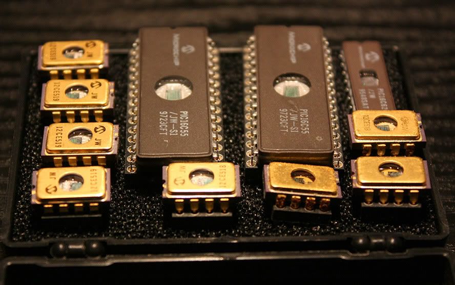
Anyway, "gold" Microchips. I still have some! Here are some versions from my archive. I say archive, its a box with chips in.
General view:
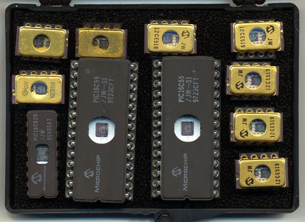
A better view, from a flat bed scanner:
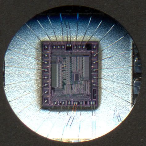
PIC16C55 close-up (If the chips are porn, is this gynaecology?)
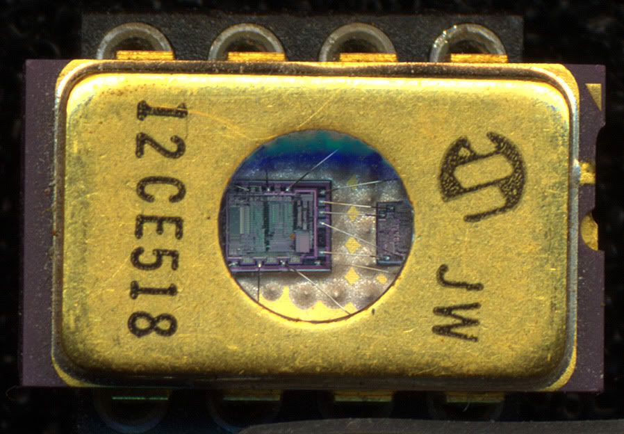
And the PIC12CE519. Note the separate memory chip packaged inside an 8 pin DIP!
I'm disappointed. I was expecting to see one taken through a microscope.
Does anyone know why some ICs have copper surrounding the window?
If you get me a photographic microscope, I'll take the photos
Found some EPROMS, here are the images. The text "fujitsu" text on one of the chips is so small that even with 10x lab stereo microscope at work, I'm just barely able to read it.
Regards,
Janne
Wow, those are fantastic! Thank you!
All of this reminds me of an article in Electronics today international about using an eprom as a custom logic chip.This was years before pics or such like and the idea was to replace TTL logic glue with a single Eprom.The concept was that the whole chip was programmed so that the address lines formed the inputs and the required output was read from the data lines.Speed and output power (not to mention having to assemble/ decode and write EVERY possible logic state to the eprom ensuring only valid input gave a valid output) were big drawbacks but it was an interesting idea.Any one ever done any thing similar? Think this was circa 1980/83
All of this reminds me of an article in Electronics today international about using an eprom as a custom logic chip.This was years before pics or such like and the idea was to replace TTL logic glue with a single Eprom.The concept was that the whole chip was programmed so that the address lines formed the inputs and the required output was read from the data lines.Speed and output power (not to mention having to assemble/ decode and write EVERY possible logic state to the eprom ensuring only valid input gave a valid output) were big drawbacks but it was an interesting idea.Any one ever done any thing similar? Think this was circa 1980/83
That is perfectly valid idea even for today. Actually, FPGA's work internally just like that. Typical structure of logic element in a FPGA contains 4-input LUT, which optionally feeds a D-FF. So basically, FPGA is a big collection of 16 bit RAM's which can resolve any logic function which consist up to 4 input variables, without optimization. Of course, there are other complications, like routing which make the structure more complicated, but it can be seen that having just large amount of small RAMs with DFF's one can build just about any digital circuit (combinatorial or clocked logic).
Main difficulty in EPROM times was probably that EPROMs were quite slow compared to real gates, thus they were not used very often. Compare typical access time of 100 ns to propagation delay of ordinary gate, which is in order of 5 ns, thus about 20x faster. Even modern parallel flash memories are not even near that fast.
Regards,
Janne
I Agree speed or lack of was a major drawback, add to that the "support" hardware and things got expensive quickly. Also the reliability of eproms was poor sometimes with bit errors common (mainly due to bad progammers/ erasers more than anything else). As an apprentice I remember the maintenance foreman getting in a real foul mood trying to copy a eprom and keep getting a corrupt copy even though he had washed it numerous time. His mood did not improve when I (a 16 year old 1st Year) pointed out he had not removed the sticker from the window, had o keep out of the the way for weeks

.