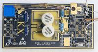
Another DIY poor man's multifunction calibrator

Based on the AD5791B.
DCV 0.1, 1, 10, 100 V. DCI 10 mA, 1 A. Ohms 1k, 10k, 100k, 1M.
LF Noise (0,1-10 Hz): 2.2...2.8 uV p-p (10V/10V), 0.4 uV p-p (0V/10V).
Laser printer film and 3M adhesive
I like to do the same thing. Print reversed on an overhead transparency sheet, spray with 3M 77 adhesive, flip over, and apply. Then the Mylar sheet protects the printing.
Laser printer film and 3M adhesive
I like to do the same thing. Print reversed on an overhead transparency sheet, spray with 3M 77 adhesive, flip over, and apply. Then the Mylar sheet protects the printing.
Yep, and a Silhouette Curio paper cutter can be used to cleanly cut the outline and holes based on alignment marks printed on the sheet, all imported via DXF if necessary.
I've also been using the Curio to cut custom gaskets for seals around connectors, CNC'd parts, etc.
today I've got 10 small cuties in my mail

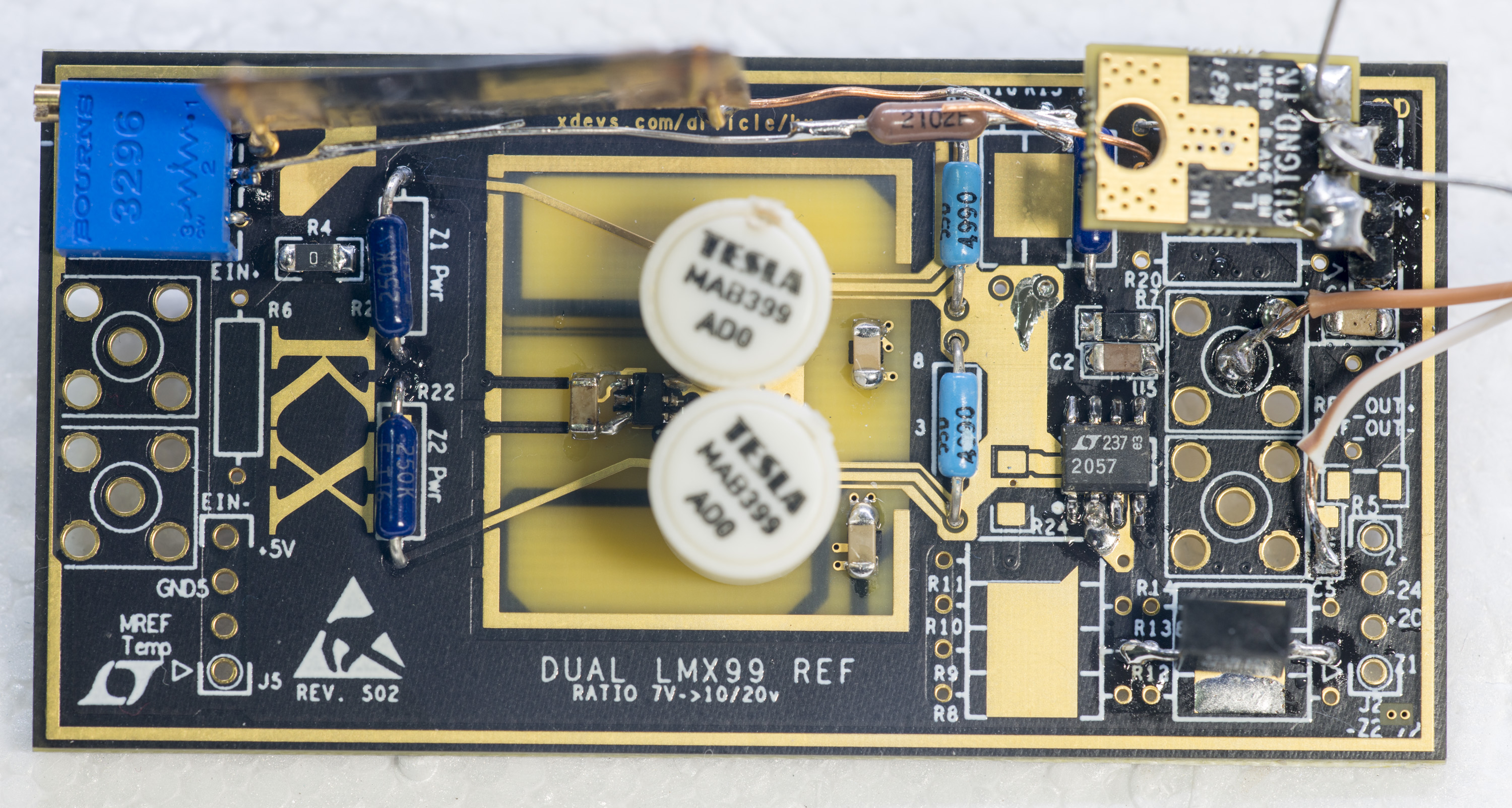
not the original LM399 but close enough (hopefully)

does anyone have experience building a reference with "eastern block" MAB399 clones of LM399 ? they have slightly higher voltage but otherwise should be quite similar. so i assume i can safely use the circuits for lm399 , the only difference would be slightly different resistor values because they have 7,25V nominal zener voltage instead of 6,95V.

Hmm, what these could be?
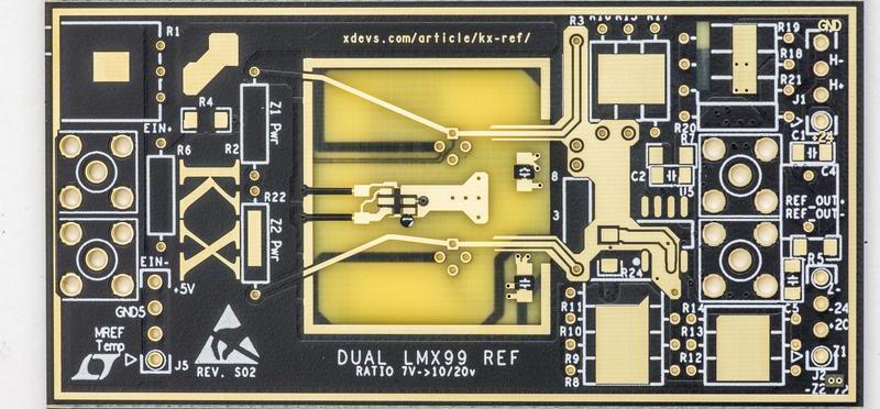
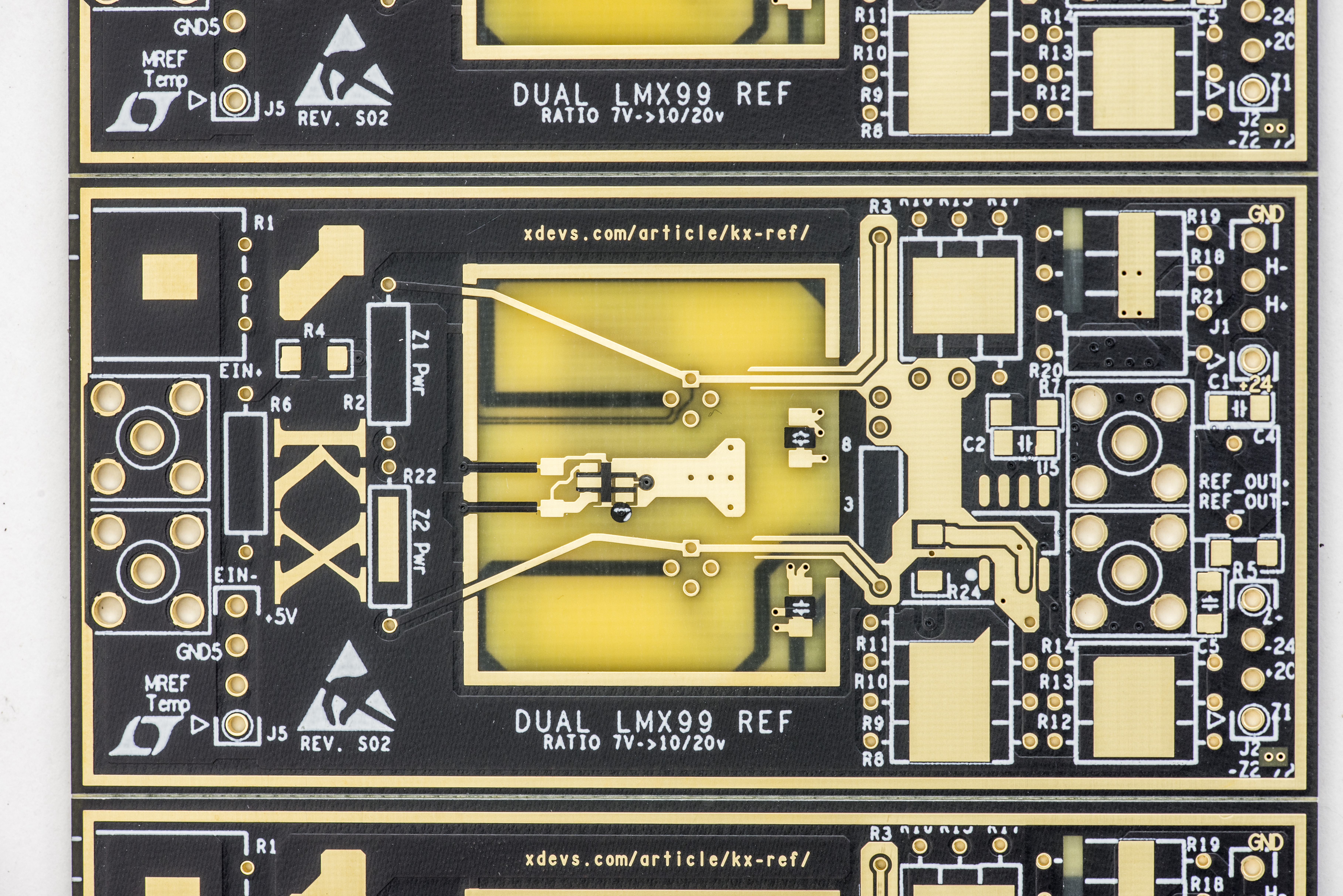
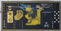
Schematic is same as on original LM399 boards I had, but layout was slightly revised. Both LMx99's are to be assembled on top side now.
As often, not without minor mistake, such as missing silkscreen for LMx399's

TiN, I never understood how the Bourns trimmer was connected. It just seems to be hanging in the breeze?
Also this circuit should work with a single LM399? Did you find the use of two of them really worth it? (Though Linear does supply 2x for free as samples of course!

)
Yes, it's not connected to anything. I just think that leaving empty PCB space is a crime

.
Idea (bad one?) behind that is that during debug/tweaking you may want to put a pot there and wire to any fixed resistor in circuit, so you can tweak it to some required value for test. Then once you get the value, pot removed and proper fixed resistor installed instead.
And yes again, circuit will work just fine with single ref. Zener outputs combined together via R3 and R23 to REFIN node of scaling opamp.
There is also possibility to measure both zener outputs via sense outputs (Pin 1 and Pin 4 on J2 connector for top zener, and two tiny exposed vias in bottom right corner for bottom zener).
Schematic is same as on original LM399 boards I had, but layout was slightly revised. Both LMx99's are to be assembled on top side now.
Hello,
that reminds me of a "event" that I had recently with one of my LM399´s:
I recognized a large drift on my LM399#2 of about 1.5 ppm within 3 days.
I then recognized that I had put the LM399#2 accidently up side down after a measurement.
When putting back to normal orientation, it needed 2-3 weeks to get back to the
previous reading.
So it might be better not to put the LM399 on the bottom side.
(I dont know if it would stabilize in this orientation).
With best regards
Andreas
To my shame, I never really tested LM399-based ones. Just built few boards to test overall function, but no ppm-nitpicking was done.
Time to correct this.
Well, looks like I may move into this adventure to check my K2000.
Since I can´t find any cheap lab around here, official or amateur.
I wish I live near TiN. :-)
Hello All,
I have 16 pcs LM399 that I connect to 30v supply for heater and cheap 30K ohm 20ppm resistor for zener after 6 month I found 4 of them are very close the difference about a few uV (according to my 3478A) and then after another 3 month I found the difference between them are 2uV.
My Initial plan are put them in condition like that for aging purpose before I can buy a decent resistor for 10v standard but then I realize I maybe made a mistake, I need to de-soldering and solder again and I read somewhere in this thread that procedure will cycling the aging process again ?
How long I need to aging this LM399 with lets say edwin resistor before I can calibrated it against "real volt standard"
Thank You
how long I need to aging this LM399 with lets say edwin resistor before I can calibrated it against "real volt standard"
Hello,
this is very individual on the LM399 sample.
Some devices need only 1-2 kHr to stabilize, others need up to 6-12 months (and some stabilize never).
You should make yourself a drift limit (per month or per kHr) and then decide when it is time to calibrate.
A good device will stabilize to around 1-2 ppm/year.
See also diagram here:
https://www.eevblog.com/forum/metrology/lm399-based-10-v-reference/msg836912/#msg836912With best regards
Andreas
Hi Andreas and Diligentminds,
Thank you for your time to respond.
I believe time and patient is our enemy for voltage reference.
and for resistor type I prefer use Edwin resistor because the price and availability is best in this parts of the world except for my LTZ1000 I already wait for 3 month for my vishay but I think I still need to wait it looooonger.
btw I just to made sure for one thing. are some one have experience about aging for LM399 or LTZ1000 with "whatever resistor You have" and then when You can get the "proper" resistor are they need to re aging again like a brand new parts ?
Thank You
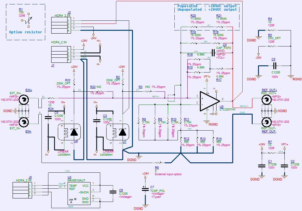
I'm trying to follow TiNs LM399 circuit and scratching my head. There are fairly specific resistor networks used for the op-amp gain but they don't add up?
e.g.
RG1 is made of 4 x 3.75K (R8-R11) in parallel which are in series with 3 paralleled 466 ohm (R12-R14) = 1093 ohm in total
RF1 is made of 2 x 16.5k (R18,19) in series which = 33k ohm for the 20V gain, or is in parallel with 2 x 11.655k (R20,21) which = 13.66k for the 10V gain.
Calculating gain 1+RF1/RG1 gives 31.19 or 13.5 for the 20V and 10V options respectively which are totally out of bounds.

I'm sure I must be thick and am missing something obvious, but I've looked through the thread and can't find anything
TiN or anyone please explain and put me out of my misery
IIRC, Plesa made some of these boards?
The way how the current to the LM399 reference is provided looks suspicious. AFAIK the resistors that provide the current (R15 and R16) should go directly to the LM399 and not to the point common to both. As shown the circuit should not work well - its essentially only one of the LM399 active. With the extra positive feedback, the divider also can die different.
As for the output, i would have preferred an extra isolation resistor, so the output can stand a capacitive load.
Also having filtering at the (+) input of the OP might be a good idea.
I figured I would let that stuff pass for now. I just don't understand how the RF/RG resistors which seem to be very specifically tuned can possibly work. I mean I get stupid gains of >200V or >90V which are just not possible.

The zener current feed R15-R17 is 7485 ohms, and each LM399 has their own 542 resistor to balance things out, so 8027 ohms. With a 20V output that would give 1.6mA to the zeners. 10V only 0.4mA. There are also the optional 200k bias resistors R2 and R22 which could donate 85uA?
I'm not sure of the -24V supply either, but that seems to be an option R5.
But I'm pretty much not an analog guy and am probably making a fool of myself

With all the resistors populated the amplification does not look right, in addition to using negative and positive feedback together. Sometimes the many parallel resistors can be just optional for variations or maybe different sizes.
Normally it also would not make sense to have so many resistors in parallel and than use different values.
If at all it might be useful to use the same type of resistor several times to get similar properties or reduce the BOM. So for the 7 to 10 V step something like using two resistor in parallel again one of the same to get the amplification of 1.5 as a first approximation and than only add one in parallel to the two to adjust to the right value.
The funny way to provide the current also seems to be in the board, just in the schematics.
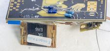
Well, you guys got me out into the light. I assembled board for test, as I really don't remember any thought when I draw this thing 2 years ago.
1. There is large impact from variable input voltage. Tens to hundreds ppm on output per 1V.
2. I got now why current supply to zener must be two separate resistors, fixed in hw now.
3. Resistors values are incorrect, they need to be matched specific to used LM399's. Currently for test I used 10K + network with total R=4k0855 to get 10V
Btw, even with these mistakes/errors seem to get result TCV about 0.9ppm/K:
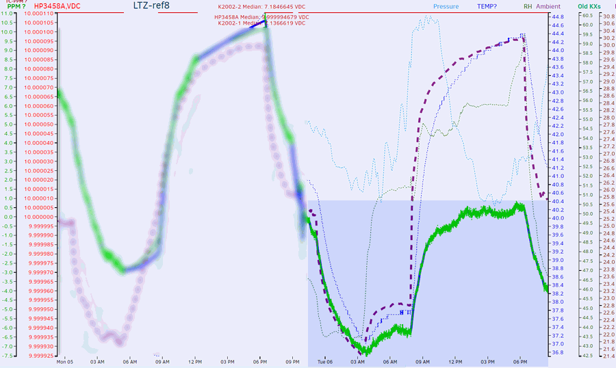
My datalog python snake was running ACAL DCV on 3458? for each change of temperature >0.3K, to remove DMM's TCV (which is ~0.3ppm/K on my box).
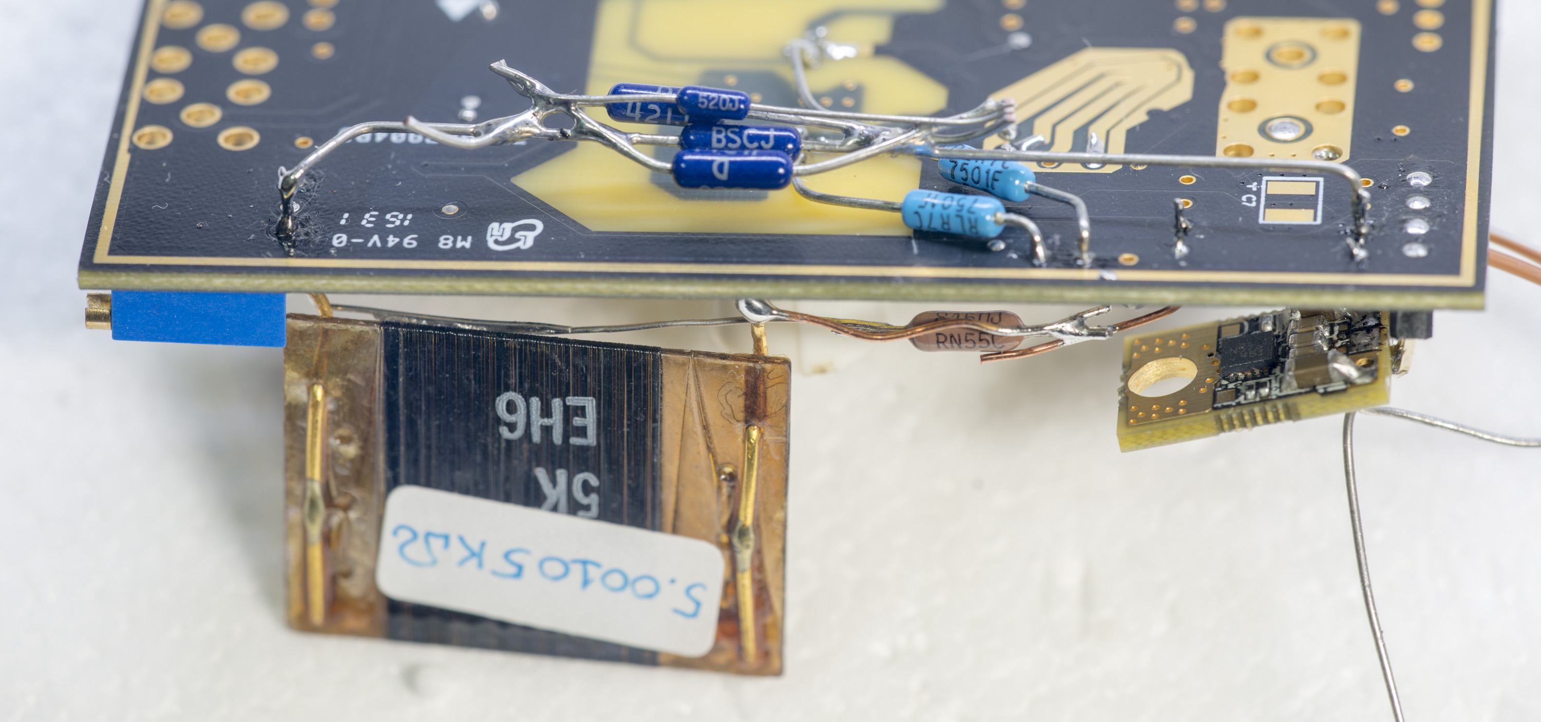
Board itself with bodges:
Let increase current for each zener to ~1.5mA (2K resistors) and test again
With the LM399 it does not really help to increase the reference current. The reference is not just a zener, but a circuit that sends a fixed current trough the actual zener and the rest only flows through parallel transistors.
So it is mainly a thermal effect from an increased current.
If the two references are close in voltage, the circuit with just one resistor for the current might still work somewhat, with slightly uneven current for both. But the it should be more sensitive to the resistors (that set the current). In the correct circuit the resistors to set the current and those to average between the 2 are not critical.
I don't think there is a big need for an extra low noise voltage regulation in this circuit. By far the dominant noise source are the two LM399 followed by the LTC2057. At least the higher frequency (e.g. > 200 Hz) noise of the reference could be filtered with a capacitor from the (+) input of the OP to ground.
With 2K current feed resistors Vz for top one is 7.07705V, bottom 7.06236V, average output after pair of 499 resistors is 7.069731V.
LDO is to keep input VCC to module stable for now at +15V.
Just another DIY poor man's selfcal DVM & voltage/resistance calibrator
ADS1256+
AD5971B AD5791B
1 ppm INL, 0.25 ppm p-p noise (DCV output), 3 ppm INL (DCV input).
Just another DIY poor man's selfcal DVM & voltage/resistance calibrator ADS1256+AD5971B
1 ppm INL, 0.25 ppm p-p noise (DCV output), 3 ppm INL (DCV input).
That looks much better than a poor man's DIY.
Very nicely done.
That is really well done.
Just another DIY poor man's selfcal DVM & voltage/resistance calibrator ADS1256+AD5971B
1 ppm INL, 0.25 ppm p-p noise (DCV output), 3 ppm INL (DCV input).
Looks very good, thanks for sharing
but where did you hide the LM399.
In one of the black boxes near the statistical divider?
With best regards
Andreas