-
Inductor saturation tester, alternative route to dump the excess energy ?
Posted by BravoV on 31 Dec, 2012 21:06 -
After reading this excellent thread made by jahonen -> https://www.eevblog.com/forum/projects/inductor-tester/ , curious if it is workable to dump the excess energy from the inductor during the discharge cycle that will go through the lower mosfet into light bulb instead of wasting it by heating the poor mosfet and the sense resistor if without the bulb ?

We don't need to measure or observe the discharge cycle anyway, cmiiw.
-
Try to put the light the other side of the mosfet so it stays saturated.
-
Ahh.. thanks a lot SeanB, apparently I forgot the lesser Vgs caused by the bulb's drop out voltage when discharging, and eventually will cause the fet to heat up more in less saturated state, noob mistake.

So is this workable ? Did I miss anything ? -
Hi group,
Here is a slightly different idea. The inductors are place in a asymmetric bridge. This allows the energy in the inductor to be recovered and returned to the supply. This allows testing of high current inductors with a small bench supply. The bench supply only has to supply the circuit losses.
I have attached the LTspice model if you want to play around.
Note: in the LTspice model the inductors do not have their saturation characteristics modelled.
Happy New Year !!!
Jay_Diddy_B ( I am in disguise -> O0 )
-
I wouldn't be worried about heating the mosfet or the sense resistor, but the main advantage would be faster current decay if one could allow higher voltage across the inductor. In principle you could do that but the mosfet driver doesn't like that the switch node goes very negative.
Of course, one could make much simpler circuit by leaving just the bottom mosfet and putting the sense resistor between mosfet source and ground. The inductor under test would then lie between positive supply and the mosfet drain. The main disadvantage would then be that the fet gate charging spike would also be measured. But then one could put a diode from mosfet drain to the cap bank, to recuperate the stored energy back to use (think it as a boost converter boosting its own supply voltage!). Also, the gate driver could be simpler then. With this configuration, one could use more elaborate high-side current sense amplifier, to avoid measuring mosfet gate current.
Regards,
Janne -
Here is a slightly different idea. The inductors are place in a asymmetric bridge. This allows the energy in the inductor to be recovered and returned to the supply. This allows testing of high current inductors with a small bench supply. The bench supply only has to supply the circuit losses.
Hmm.. great idea, dumping the energy back to the bulk caps, never thought of that, thanks a lot !
Now time to digest & understand it thoroughly.
Quick question, for an accurate result reading, what should I aware of compared to the original one ?
@Janne, its great to see you here, thanks ! I launched this thread cause don't want to "contaminate" your fine thread with noob questions like this.
 Of course, one could make much simpler circuit by leaving just the bottom mosfet and putting the sense resistor between mosfet source and ground. The inductor under test would then lie between positive supply and the mosfet drain. The main disadvantage would then be that the fet gate charging spike would also be measured. But then one could put a diode from mosfet drain to the cap bank, to recuperate the stored energy back to use (think it as a boost converter boosting its own supply voltage!). Also, the gate driver could be simpler then. With this configuration, one could use more elaborate high-side current sense amplifier, to avoid measuring mosfet gate current.
Seriously, I'm having a difficulty to visualize the circuit and doubting my self, would you mind to make some quick scratch of the circuit in picture from above description please ?
-
Hi,
The circuit that Jahonen proposed looks like this:
This circuit does not recover the energy stored in the inductor. The energy is dissipated in the winding resistance of the inductor and the diode.
The duty-cycle should be low, to allow the inductor current to reset and control dissipation in the diode.
If ypu are testing small inductors it is not important to recovery the energy. As the energy in the inductor increases it becomes increasingly important to recover the energy to reduce power dissipation.
This circuit and the bridge circuit, that I proposed, include the MOSFET gate current on the sense resistor. Fortunately, there is no gate current when the inductor saturates.
Inductor saturation is typically defined by a 30 - 40% change in inductance. In the tester this is seen as a change in dI/dt.
For the intended purpose these testers will be accurate enough.
Jay_Diddy_B
-
Hi,
The circuit that Jahonen proposed looks like this:
This circuit does not recover the energy stored in the inductor. The energy is dissipated in the winding resistance of the inductor and the diode.
The duty-cycle should be low, to allow the inductor current to reset and control dissipation in the diode.
Yes, I realized that after I posted my message and turned off my PC. Naturally, one needs a some form of a bridge circuit to recover the energy, like in motor drive circuits.
But, having used the thing in practice with various bench supplies, even if the energy is not recovered, no need for beefy power supply as the energy required to saturate the inductor (in cases where such tester construction is applicable anyway) is quite low. Intended usage is anyway by single pulses or low repetition frequency (<10 Hz) anyway (works nicely with a DSO with averaging acquisition).
Regards,
Janne -
I like JDB's idea. It seems that it should be possible to achieve much higher pulse rates which is handy if one wants to simulate real life conditions for a particular inductor to observe temperature rise, for example.
Another handy feature would be a possibility to inject DC current into DUT. I'm going to build a circuit and check it as soon as the parts arrive. -
PS : Edited my previous post cause I just realized the H-bridge model using 4 mosfets wont work, silly me.
JDB, your idea is really great after observing the simulation you provided, what kind or type of mosfet drivers needed for this concept below to work ? The same one used by Janne's circuit like IR2011 is enough ? Btw, both are N-Mos, no P-Mos.
@mazurov, thats great, please share once you built it !
-
Hi BravoV and the group,
The MOSFET driver required is a little bit different than a normal half-bridge driver.
For my circuit to work properly, both of the MOSFETs in the bridge have to be ON at the same time. Normally you would not want this condition and the circuit would have dead time between the top and bottom MOSFETs.
The other issue with MOSFET drivers like the IR2011 is that they require the circuit to be switching to provide a charge pump action to drive the top MOSFET. In this application, it is desireable to be able to do a single pulse or low repetition frequency.
I chose a P Channel MOSFET for the top MOSFET. This allows me to drive it with the level shifter M3 and Q1. As originally drawn there are some limitations. The supply voltage must be high enough to turn on the MOSFETs but less than Vgs max (typically 20V).
I deliberately chosen not to drive the MOSFETs very hard, that is why I have 22 ohm series resistor on their gates.
A 555 will provide enough gate drive for this application.
I would also recommend that you place a 51 ohm resistor in series with the output from the sense resistor. Make the connection to the scope with 50 Ohm coax and terminate the scope input with a 50 Ohm resistor.
This will divide the signal amplitude by 2, but you will get much cleaner waveforms.
Jay_Diddy_B
-
@JDB, thanks alot for your help, this has been very educational, at least for me.
The MOSFET driver required is a little bit different than a normal half-bridge driver.
You know what ? Your comment above made me read tons of those mosfet driver's datasheets & appnotes from various manufactures, and learned a lot, yeah, those dead time and also the one with charge pump with the boost cap needs quite some high frequency in order to charge the gate driver strong enough.
For my circuit to work properly, both of the MOSFETs in the bridge have to be ON at the same time. Normally you would not want this condition and the circuit would have dead time between the top and bottom MOSFETs.
The other issue with MOSFET drivers like the IR2011 is that they require the circuit to be switching to provide a charge pump action to drive the top MOSFET. In this application, it is desireable to be able to do a single pulse or low repetition frequency.
While in our case here, the signal might be running at quite low frequency and also very low duty cycle, it might not be enough for the charge pump to work effectively, correct me if I understand it wrongly.
Ok, then mosfet driver is out.
I chose a P Channel MOSFET for the top MOSFET. This allows me to drive it with the level shifter M3 and Q1. As originally drawn there are some limitations. The supply voltage must be high enough to turn on the MOSFETs but less than Vgs max (typically 20V).
I'm curious on the reason why you prefer not to drive the mosfet very hard like Janne did ?
I deliberately chosen not to drive the MOSFETs very hard, that is why I have 22 ohm series resistor on their gates.A 555 will provide enough gate drive for this application.
I assume you mean using the bi-polar version of 555 instead of cmos version right ? Cause it will be driving the gate of M2 and M3 mosfet.I would also recommend that you place a 51 ohm resistor in series with the output from the sense resistor. Make the connection to the scope with 50 Ohm coax and terminate the scope input with a 50 Ohm resistor.
Yes, will do since my scope has 50 termination mode, thanks for the reminder, and note to others that have low end dso, most of them don't have 50 ohm termination.
This will divide the signal amplitude by 2, but you will get much cleaner waveforms.
Another question, the M3 doesn't need to be high power mosfet right ? -
IR2011 does not have any cross-conduction protection or integrated dead time so you can actually turn both outputs on simultaneously, and it should work fine as posted by BravoV. Only thing is that it needs a path to charge the bootstrap capacitor. Otherwise, the high side driver fails to turn on due to UVLO. Also, if you don't use four mosfets (i.e. full bridge configuration), and two IR2011s, then make sure that the diodes used for energy return are beefy enough, they should be able to withstand the maximum current in the inductor.
Regards,
Janne -
Hi BravoV and the group,
How hard you need to drive the MOSFET depends on a how short a pulse you need, or how small an inductor you want to test. The advantage is that by not driving the MOSFET hard, the gate current is insignificant when looking at the source current.
MOSFETs have steadily improved over the years if you look at a figure of merit Gate charge / RDSon.
The other argument is power dissipation. Power dissipation increases with soft gate drive. But since, we are doing low repetition frequency, I am not too concerned about switching losses.
The Bipolar version of the 555 is preferred. It has the capability of +/- 200mA of drive. The gate drive could be increased with a complimentary emitter follower if required. I am trying to use generic parts, that people should have in their junk boxes or that easy to get.
Thank you for clarifying the 50 ohm termination.
M3 is a small signal MOSFET (2N7002, BSS170 etc.)
I am going to try an build the circuit over the weekend.
Jay_Diddy_B
-
IR2011 does not have any cross-conduction protection or integrated dead time so you can actually turn both outputs on simultaneously, and it should work fine as posted by BravoV. Only thing is that it needs a path to charge the bootstrap capacitor. Otherwise, the high side driver fails to turn on due to UVLO. Also, if you don't use four mosfets (i.e. full bridge configuration), and two IR2011s, then make sure that the diodes used for energy return are beefy enough, they should be able to withstand the maximum current in the inductor.
Like this ?
Ok, I'm a bit confused here, especially the decaying route pointed by the dotted arrow, once the energy in the inductor depleted, isn't that same path will charge the inductor again if we don't control the timing precisely ?
Also about the charge for the bootstrap capacitor, on my previous topology using diode for the decaying route instead of mosfets, any idea how to solve it without getting the circuit grows overly complicated ?I am trying to use generic parts, that people should have in their junk boxes or that easy to get.
I am going to try an build the circuit over the weekend.
This is great, especially using ordinary easy to find components , can't wait to see your implementation.
-
Like this ?
Ok, I'm a bit confused here, especially the decaying route pointed by the dotted arrow, once the energy in the inductor depleted, isn't that same path will charge the inductor again if we don't control the timing precisely ?
Also about the charge for the bootstrap capacitor, on my previous topology using diode for the decaying route instead of mosfets, any idea how to solve it without getting the circuit grows overly complicated ?
Yes, it does charge the inductor again. Diodes are a good that they will not charge the inductor back but of course dissipate fair amount of instantaneous power due to the forward voltage drop. One way would be to monitor the current and stop driving those fets when the current turns negative, but I guess that is quite complex solution.
I think that a suitable resistor in parallel of the left diode will solve that charging problem, provided that you are not in a hurry to charge the capacitor, i.e. the pulse frequency is low enough, so that there is enough time to charge the capacitor before the next pulse.
Regards,
Janne -
Hi Group,
I have been busy building. Here are the results of my efforts.
Schematic:
Board Layout
Milling the circuit board on a LPKF Protomat 60
The finshed board after tin plating
The assembled board
Testing a 22uH Inductor. The scaling factor is 10mV per Amp. The saturation can be clearly seen at around 3.2A
With a Tektronix TCP202 current probe (red trace). The difference between the trace is MOSFET gate current.
I was driving the test circuit with a 10V power supply. The pulses were supplied by an HP8112A pulse generator.
Improvement:
An inverting stage should be added to the input.
I have attached a pdf version of the schematic.
Regards,
Jay_Diddy_B ( I am in disguise -> O0 )
-
Wow .. so fast, I never expected you came out with so nicely built circuit so soon ! Btw, feel so jealous seeing that Protomat 60, its one of my dream machine.

To be honest, the reason I started this thread was to start learning and trying to build much simpler one compared to Janne's nicely built, and the idea of dissipating the excess energy from the inductor popped out while learning it.
Now, I'm convinced and definitely I'm going to build it, thanks to you JDB and Janne too.
In my version, the plan is to build a standalone unit with the signal will be supplied by using a much simpler pwm generator like using a 555 for generating the triangle wave and a comparator maybe like LM311 with a pot for duty cycle adjustment in order to get a really small pulse at low frequency. This should be workable right ?
Those scope shots are really nice, and if its not too troublesome, please shorten the pulse maybe like 10us to get close to the "knee" without the signal shooting up too high to show the complete cycle nicely in the scope screen. And from your traces, it looks like the inductor decaying speed was so fast. Also how is the discharge cycle when the inductor was releasing the energy ? Again, if you had a chance, please do trace the TP4 point, curious to see how the voltage jumps at the point during the decay period.
Off topic, your TCP202 decaying red trace is slower with a slope compared to the black inductor trace which is straight vertical, why is that ? The probe's limitation ?
Again, thank you so much JDB. -
Hi BravoV and the group,
The LPKF Protomat is a great tool. It gets (three thumbs up)
Here are some more screen shots from the oscilloscope that further explain the circuit action.
This condition is essentially the same as the earlier screen shot.
In this first picture I have 'zoomed out' to show the more of the cycle. The upper trace is the output from J1. The sharp edge is caused when the MOSFET Q2 is turned off, it is no longer possible to measure the inductor current.
The Tektronix TCP202 current probe is on the inductor, so it is able to measure the inductor current as the energy is returned to the supply via D3 and D4.
The lower Trace is TP4, one side of the bridge.
I have now reduced the width of the pulse from the pulse generator, keeping the scope settings the same.
You can no longer see the inductor going into saturation
In this screen shot I have 'zoomed out' further and increased the repetition frequency. I have also added TP3.
The voltage across the inductor is the difference between the TP3 and TP4 waveforms. Again, this shows how the energy is recovered.
The current draw from the 10V power supply from this test was 0.058A, which is 0.58W and this includes all the power consumption in the gate drive circuitry.
Jay_Diddy_B ( I am in disguise -> O0 )
-
Thanks for the scope shots JDB (or what ever your real name is) !
In this first picture I have 'zoomed out' to show the more of the cycle. The upper trace is the output from J1. The sharp edge is caused when the MOSFET Q2 is turned off, it is no longer possible to measure the inductor current.
Again, beginner's mistake, silly me.
The voltage across the inductor is the difference between the TP3 and TP4 waveforms. Again, this shows how the energy is recovered.
During the decaying period, once the inductor's voltage (minus diodes drop out) is equal to power supply rail, the inductor will self dissipate the rest of it's own excess energy through the ringing as observed at the scope shot, am I correct ?
Just curious and purely academical here, curious in ball park number on how much percentage of the energy left in percentage of total only at that ringing period ?
Still learning, hope you're not bored to death entertaining my noobness.The current draw from the 10V power supply from this test was 0.058A, which is 0.58W and this includes all the power consumption in the gate drive circuitry.
I'm aware of the energy required to charge those big caps when the circuit was turned on for the 1st time, but lets ignore this initial state, from this result that this circuit draws only 58 ma at 10 volt is pretty low isn't it ? This is valuable info, so I don't need a beefy power supply.
Another question
Is it easy to separate the supply of the driver (inc the pwm generator) in the yellow shaded area from the green one at the below pic ?
The reason is, say for an inductor with high inductance and high current saturation, this will have a really slow di/dt or shallow loong trace, so the easier part is to crank up the supply voltage to speed up the di/dt, and vice versa like small inductor with low inductance that has really steep di/dt, reducing the supply voltage will make the measurement easier.
Of course there is a reasonable min and max test voltage for the inductor say like starting from 5 volt up to maybe 30 volt ? Or what ever range that you think is possible without over complicated your design ?
Thanks in advance, JDB.
PS : Suggesting you to attach any pictures at this forum like I did here, instead of using external hosting like the tinypic.com you're using, we never know what will happened in the future for this kind of hosting sites. An example what is happening with these so called "FREE" pic hosting site -> HERE.
Just use the attach feature right below the dialog box where you type your post.
-
Quote
During the decaying period, once the inductor's voltage (minus diodes drop out) is equal to power supply rail, the inductor will self dissipate the rest of it's own excess energy through the ringing as observed at the scope shot, am I correct ?
Just curious and purely academical here, curious in ball park number on how much percentage of the energy left in percentage of total only at that ringing period ?
Still learning, hope you're not bored to death entertaining my noobness.
There is not very much energy left at all. The evidence for this is the Tektronix TCP202 shows essentially zero current. What is happening is that the inductor is ringing with the capacitance of the diodes and the output capacitance of the MOSFET.QuoteI'm aware of the energy required to charge those big caps when the circuit was turned on for the 1st time, but lets ignore this initial state, from this result that this circuit draws only 58 ma at 10 volt is pretty low isn't it ? This is valuable info, so I don't need a beefy power supply.
Absolutely, I had my Power supply current limit is set to 200mA.
Varying the Supply voltage.
As I have designed the circuit, it is all dc coupled. I also designed the circuit using commonly available parts.
I have given some thought to using transformer coupled gate drive. This means using an non-junk box part, I could probably find some thing on Digikey. If I did this it would be really easy to separate the supplies.
Stay Tuned.......
Jay_Diddy_B
-
Varying the Supply voltage.
As I have designed the circuit, it is all dc coupled. I also designed the circuit using commonly available parts.
I have given some thought to using transformer coupled gate drive. This means using an non-junk box part, I could probably find some thing on Digikey. If I did this it would be really easy to separate the supplies.
Stay Tuned.......
Great .. , looking forward to see the new revision and thanks for your generousity.
About transformer, I'm not scared to wind my own and will not hesitate to go thru trial & error if needed, its part my learning journey too. Btw, I have tons of salvaged inductors or ferrite cores here, and this is the sole reason why I'm interested in this circuit from the 1st place. Hopefully you will assist me in making one if required.
About digikey, though I can afford it, a fix minimum $70 just for the shipping cost alone is too much if just for few passive components
Please, apart from the required transformer, use common or easy to find components in your design if possible. -
Hi BravoV and the group,
Here is a LTspice model of an Inductor Tester with transformer coupled gate drive. The transformer allows the two supplies, one for gate drive and the other to power the inductor to be separated.
This gives these results:
I have attached the LTspice model for you to play around.
Jay_Diddy_B
-
That particular pulse transformer looks a bit limiting for this kind of application since it limits the maximum pulse width by saturating itself. When that happens, the gate drive voltage collapses. Maximum volt-µsecs is specified as 95 V*µs, so at least I think it is a quite limiting for this kind of application (12 volts gate drive supply means that maximum pulse width attainable is 95 V*µs/12 V = 7.9 µs if we go by the specifications).
For example in this measurement I needed several tens of µs of pulse length before the saturation occurs (I believe that the supply voltage was 30 V). Note also the di/dt math trace which can be used to calculate the inductance for a particular inductor current.
I'd prefer that high-side gate driver, easier to use. But, it will limit the gate drive pulse length also, but what I measured the maximum pulse length for the values I have in my tester is several milliseconds before the high-side capacitor runs dry and UVLO kicks in, and is easily increased by increasing the value of the bootstrap capacitor.
Regards,
Janne -
JDB, thanks for the new revision, but I just knew that the issue Janne's brought out about the max pulse length, how to overcome this if we need longer pulse ?
Thanks Janne, I tested JDB's new revision at ltspice using longer pulse (40 us), apparently the gate voltages collapsed sooner below 10 volt at < 10 us as you stated, these are the gate-source voltages for both mosfets M1 and M2.
-
Well if you want to use a gate transformer, then besides using a some kind of charge pump technique (this would make the pulse somewhat difficult to control) to reduce duty cycle problems, there is no other way to avoid saturation problem than just increase the primary inductance to avoid saturation problems. You can test this by increasing all inductances by factor of x, that way the maximum pulse length is also increased by a factor of x.
Regards,
Janne -
Well if you want to use a gate transformer, then besides using a some kind of charge pump technique (this would make the pulse somewhat difficult to control) to reduce duty cycle problems, there is no other way to avoid saturation problem than just increase the primary inductance to avoid saturation problems. You can test this by increasing all inductances by factor of x, that way the maximum pulse length is also increased by a factor of x.
To be honest, I'm not expecting that this is becoming complicated because of my wish to be able to adjust the test voltage on the inductor.
Still hoping that JDB can come out with solution, of course still wishing if possible to use junk box type components, then it will be the best.
@JDB
What if the driver part is using higher supply voltage ? Say like 20 or even 24 volt ? Will this condition make it easier to design the circuit but yet simple ?
Don't have any problem at all to make a dedicated high voltage DC supply for the driver part while leaving the inductor test voltage to be supplied by a bench PSU so the voltage can be adjustable.
Again, as an EE wannabe I'm not sure what I'm talking about here, just a wild idea.
-
If you want it just to be simple, and do not care about initial gate current glitch in current sense, why not just do it this way? As you can see, even with no supply at all and just charged caps, you can fire quite a few pulses before the caps become discharged, so there is plenty of time to charge the discharge bank capacitors between pulses. This way, you can adjust the current decay rate by adjusting R2, but of course keeping eye on how high the voltage becomes on fet drain.
Anyway, in practice even without the current decay speedup, the recovery is fast enough to have results in reasonable time period.
Regards,
Janne
-
Another version with an experiment with energy recover with a transformer. Don't know if that transformer contraption could actually work.
Regards,
Janne
-
Hi Group,
I have been busy building. Here are the results of my efforts.
Schematic:
This looks like a hazardous circuit to use. If you set the input pulse duration too long it will blow up as there is no protection circuitry to limit the MOSFET current when the inductor under test saturates. At a minimum I'd power it with a current-limited bench supply. -
Hi group,
I have had another go at designing the circuit. I want to thank everybody for their inputs. This is a tricky circuit to design.
This concept includes:
1) The control power supply and the power supply for the bridge are separated. The bridge supply can be set to from 0.5V to 30V (upper end depends on component voltage ratings.
2) The circuit will work with pulse widths from around 0.3us to 0.5ms
3) The circuit includes over current protection. As presented the current trip is set to approximately 10A
4) No exotic components are used.
I have attached the LTspice model for those wanting to test the circuit.
Edit: Q8 was drawn upside down. I have removed the LTspice file. See the next entry
Jay_Diddy_B
-
Hi,
I made a small mistake. Q8 was drawn wrong.
I have fixed my mistake.
The corrected files are attached.
Jay_Diddy_B
-
@Janne,
The chart is proofing that the 2 x 2200 uF caps alone is plenty, still capable of serving many pulses and yet still strong, not bad, learned something new, thanks. Your second concept design using transformer looks interesting and really intriguing , I might try it once I have a working one with the "traditional" design ! This looks like a hazardous circuit to use. If you set the input pulse duration too long it will blow up as there is no protection circuitry to limit the MOSFET current when the inductor under test saturates. At a minimum I'd power it with a current-limited bench supply.
Thanks for the reminder, JDB already made this into the new revision. The plan is to use a bench PSU that capable of CC.
I guess there are advantages too to leave this circuit like current state which is not a complete ready to build circuit, like no pwm generator part, no power supply section and a bit vague on high current components like mosfets and power schotky diodes, hopefully at least this will lead others (hobbyist/enthusiast grade) that is planning to build this to learn and understand how it works 1st and the risk involved.
This concept includes:
1) The control power supply and the power supply for the bridge are separated. The bridge supply can be set to from 0.5V to 30V (upper end depends on component voltage ratings.
2) The circuit will work with pulse widths from around 0.3us to 0.5ms
3) The circuit includes over current protection. As presented the current trip is set to approximately 10A
4) No exotic components are used.
Looks great JDB, thanks alot, ha..ha.. that max pulse length 0.5 ms is overkill, but its nice.
I can see you've increased the sense resistor ten folds for the current limit mechanism to be able to kick in.
In my build, I think I will skip that current limit section and going to use 0.01 Ohm and coupled with an op-amp buffer like Janne did for the current sensing signal to the scope. Planning to use a jfet LF411 (I got many of it in my junk box and also it has offset adjust) as the buffer, this should be good enough right ? Yes, it will have the negative rail provided by ICL7660 charge pump.
Just glad we are at this stage now that we're able to adjust the inductor testing voltage, just happy that this EE wannabe's idea is workable, again thanks to you.
Ok, I'm going to draw the circuit of my version, and I guess I will bug you again for the approval stamp.
-
Hi group,
It is time to report on the Inductor saturation tester project. I have built a new version.
Here is the schematic:
Here is the PCB Design:
And the construction:
Here are some of the test results:
The red trace is the inductor current. The blue trace is the output from the inductor tester 50mV/A. The black trace is the input from the pulse generator.
Current limit at 9.4A
Low voltage operation, long pulse operation. The voltage applied to bridge was 0.7V
High speed 1us pulse. You see that one side of the bridge is delayed by about 300ns. For this screen shot 30V was applied to the bridge.
I have attached a pdf of the schematic.
Jay_Diddy_B
-
Here is the schematic:
Hi
R8 is going to dissipate a lot of power when your two-transistor over-curent SCR fires. You'd be better off using the SCR to pull the collector of Q4 low. -
I made this one. I had problems at first with the powersupply. Needed a very big one to make sure it did not started to oscillate.
But Jim Williams had one in an application note and to his idea I added the diode and RC.
No it behaves wonderfull and I can test inductors without problems.
It is in a plastic box, no heavy heatsinks.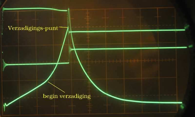
1A/div
http://www.pa4tim.nl/?p=1859 here the rest of the pictures. -
Hi PA4TIM,
The circuit that you show certainly, works as evident in the scope photograph that you provided.
The Energy that is stored in the is = 1/2 L I2
The power that is dissipated in the resistor R2 is = Frequency x 1/2 L I2
Where
Frequency equals the repetition rate of the test
L = the value of the inductance in Henries
I = peak inductor current
Some of the power will be dissipated in the MOSFET Q1, depending on the speed of the switching.
V2 can be made variable. Lower values of V2 can be used for smaller value inductors.
The current probe can be replaced with a current transformer, of the type found in switch mode power supplies.
The complexity of the circuit that I presented comes form the original posters request to recover the energy. My circuit will work with a very wide range of inductor and saturation current values.
You could put a current sense resistor between the negative end of the power supply and ground. The voltage across the resistor can be used to display the current.
Regards,
Jay_Diddy_B -
It is time to report on the Inductor saturation tester project. I have built a new version.
Duh ... ok, this is a bit of embarrassing, I'm the who started this thread still haven't started anything yet, while you already built your 2nd one. 
Low voltage operation, long pulse operation. The voltage applied to bridge was 0.7V
This ... exactly as I was expecting, with the low voltage, the trace is not straight anymore and becoming more like a curve, thanks a lot for this particular scope shot. Also this makes me to put a note when designing the pcb to add a reserve space for more additional bulk caps just in case I will be doing lots of low voltage testing. High speed 1us pulse. You see that one side of the bridge is delayed by about 300ns. For this screen shot 30V was applied to the bridge.
This one is interesting, but to be honest I'm lost, are you saying that when at the ON time, the lower fet was turned off late about 300ns compared to upper one ? A quick scratch on that shot using ms paint job to explain it if not troubling you too much.
JDB, as the pulse generator, my plan is to use the 555 as the oscillator (with pot for freq adj.) which generates a triangle, then this signal will serve as SYNC signal to the scope and also to a 311 comparator with pot for duty cycle adjustment. The noob question is, does the 311 output (with pull up resistor say 1 K) beefy enough to be connected to the input (R14) ? R13 will be omitted since its no longer needed.R8 is going to dissipate a lot of power when your two-transistor over-curent SCR fires. You'd be better off using the SCR to pull the collector of Q4 low.
How much power is that ? As my EE wannabe calculation, that R8 (22 Ohm) should not dissipate more than 0.3 watt, CMIIW.
@PA4TIM
The one that JDB made here returns the rest of the inductor's energy back to the voltage source (bulk caps), so overall the circuit it self will consume quite low current as JDB previous post to proof that, of course with the exception of charging those bulk caps when powering them for the 1st time.
As strange as it sounds, like Janne said, this circuit is like a boost circuit but boosting it back to it self.
-
Hi BravoV and the group,
I will answer the most important questions today.
Here is a revised schematic, with the modification proposed by GK, this removes the possibility of high dissipation in R8.
The delays in the 1us pulse are a combination of the extra propagation through the inverting stage Q9. Selecting a special transistor for this location will shorten this delay. suitable transistors are 2N2369A or BSX20. These transistors have special doping which results in very short switching times. I didn't use these in the design for a couple of reasons:
1) I was determined to use readily available parts.
2) The distortions occur after the inductor performance has been measured. Note the difference between the current probe waveform, which is measured in series with the inductor, and the current measured from the sense resistor in the source of the N Channel MOSFET. The current probe has a bandwidth of DC to 50 MHz, so the current probe is giving a true representation of the waveform.
I will post a few more waveforms when I get back in the lab.
Jay_Diddy_B
-
I like youre desing, that is not why i posted mine but I had dissipation and psu problems too at first. My 10A powersupply was not enough, i had to use a 100A PSU. But with the small changes all ks without cooling build in a small plastic cabinet and i can use allmost any psu. But I have never been over 10A for testing ( had no need for that)
A very handy piece of kit, used it always when I build a smps.
I do not measure current using probes like on the ( old) photo, this was the first version, i now use most times a Tektronix CT1 inline current probe or my P6042 that has a calibrated current/div reading. -
How much power is that ? As my EE wannabe calculation, that R8 (22 Ohm) should not dissipate more than 0.3 watt, CMIIW.
12V minus ~three Vbe's; approximately ~ 4.5W
Edit; actually it would be closer to half that as you will get a substantial voltage drop across the 2200 ohm pull-up due to the finite beta of Q1; still too high for a 1206.
-
The delays in the 1us pulse are a combination of the extra propagation through the inverting stage Q9. Selecting a special transistor for this location will shorten this delay. suitable transistors are 2N2369A or BSX20. These transistors have special doping which results in very short switching times.
Thanks for the update, regarding the Q9, how significant the difference if using 2N2369A or BSX20 ?
Also need confirmation from experts, is it good enough for this purpose to build the pulse generator using these cheap components like this ?
-
Depends on how fast the Tr of the pulses should be, they can not become faster as transistor in the compartor you used. If you want a sub-nano pulser you tie the base through 10K to gnd, 1M on the collector and the emitter to the bnc center together with 50 Ohm to gnd.
You feed the 1M around 80-110V and the bsx or 2n starts to avalance. I tried both transistors and they were close. I get a Tr under 500 ps ( it is the Jim Williams pulser) -
PA4TIM, I think you misunderstood my intention, I don't need those pico second Tr pulse, yes, I'm aware of that JW pulser, beside its not easy to control the pulse width either and make it useless for this circuit. OT, just wait for few weeks, I might build my self a < 150 ps Tr avalanche pulser, yup. not a typo, a 150 pico second rise time.

For my need, I think starting from 1 us up to few tens of us or max at 100 us is enough, also if the di/dt is too steep like small inductor, all I need is just turn down the voltage at my bench psu and vice versa for huge inductor, so I believe the pulse width range should not be really critical, just need the pot to adjust until "the knee" is starting to form, cmiiw. -
Ok, i did misunderstood it because you used that fast transistor, i thought you were going OT ;-) but now I understand.
150 ps is very fast, you need an even faster scope to do something with it ( and a long enough pulslenght) what is the purpse ? I an anxious to how you make that. -
150 ps is very fast, you need an even faster scope to do something with it ( and a long enough pulslenght) what is the purpse ? I an anxious to how you make that.
Ok, since you asked, even though out of topic.
To get the hint click -> Here , and also check the list with my name that has the suffix "BFG" on it -> Here, now you know why.
The reason is currently I'm lurking & stalking for quite sometime at local market at few used a Tek 7104 mainframes, so this 150 ps pulser might be useful for on spot checking if needed.
-
Then hou have to use a chargeline to make the pulsewidth longer. I use a 500 ps 40 MHz squarewave geberator to test high BW scopes. I can not get the 1S2 to trigger on an avalance pulser . Frequency and amplitude are too unstable. Frequency is to low for the prinitive triggering a a 1S2. Fror a 7104 it will do, but for adjusting/calibration you need a much longerpuls ( i did not get that trsnsistor to avalnce. The fastest I can make is 90 ps, the fastest pulse I build my selve was around 100 pds but that was with a thing I thought was an S-band diode but it dyed while experimenting. Later i saw a picture of something similair and that was a sort of VDR/spracgap thing ( a transient orotction) so maybe it was no diode. It was in my diode junkbox anf I just tried hoping one was a tunneldiode. Most ad no typenumbers printed on them.
-
Hi Group,
We got a bit off topic with the avalanche pulse generator.
Here is an alternative to the Pulse generator proposed by BravoV
I used two 555 timer, the CMOS version of the 555 should also work, and probably better. The first 555 is configured as a fixed frequency oscillator at around 7kHz. This could easily be made variable. This is used to trigger a 555 monostable. The monostable is configured to give pulses from 1us to 23us with a 20K pot. The LTspice shows a voltage controlled resistor. The resistor is changed from 0-20K to show the variation in pulse width.
The advantage of this circuit is there is a hard stop on pulse width.
Here are the simulation results:
I have attached the LTspice model
I have not built this circuit, so consider it experimental.
Jay_Diddy_B
-
Here is an alternative to the Pulse generator proposed by BravoV
The advantage of this circuit is there is a hard stop on pulse width.
I have not built this circuit, so consider it experimental.
Thanks for the new pulsegen circuit, yep, confirmed it has the hard stop and since its quite easy, built it in just few minutes and here are the results on the pulse it generated at the attached picture.
Pardon the rat nest breadboarding, yeah, it looks scary but it works, the pot for pulse width adjustment is not in the pic.
Scope shots, the whole signal, running approx 1.3Khz at quite low duty cycle with those floating dots represent very narrow/low duty cycle, and two last shots were the different pulse width adjusted approx. from 12 us down to about 3 us, didn't have the right pot yet.
Again, thanks JDB, now the hard part, going to build the pcb.
-
Note: in the LTspice model the inductors do not have their saturation characteristics modelled.
They can. Set the inductance to "flux=L*N*tanh(x/N)" where L = inductance and N = saturation current.
I just built this tester as noted in this thread, and BravoV (who suggested it to me in the first place) said I ought to post pictures and whatnot here, so here you go. Thank you very much, Jay_Diddy_B, this works quite nicely.
Scope captures:
1. 200uH inductor wound on improper core (high permeability ferrite toroid)
2. 1mH inductor wound on the same core
3. Inductor from #2 with the core broken and glued back together. The inductance fell to 32uH.
4. Murata 32101C (100uH 1.4A)
Modifications:
1. AC terminated the trigger input (makes it easy to just throw in a square wave without worrying about overheating the termination or having to use a big one).
3. RC (1k/22nF) snubber keeps the inductor from ringing horribly when the diodes shut off.
Those transistors and diodes hardly get warm at all.
-
Thanks for sharing this !
Damn, I'm impressed, you built it just in few hours ? I just introduced you to this circuit yesterday, did you etch the board using film transfer ?Scope captures:
Great results !
1. 200uH inductor wound on improper core (high permeability ferrite toroid)
2. 1mH inductor wound on the same core
3. Inductor from #2 with the core broken and glued back together. The inductance fell to 32uH.
4. Murata 32101C (100uH 1.4A)
On the gap matters, especially I love to salvage those big beads and turning them into power inductor, those glued core can be further "enhanced" by widening the gap like this, sometimes hundred fold increase.
The wide air gap at the left one is created using cut-off rotating wheel.Modifications:
1. AC terminated the trigger input (makes it easy to just throw in a square wave without worrying about overheating the termination or having to use a big one).
3. RC (1k/22nF) snubber keeps the inductor from ringing horribly when the diodes shut off.
Mind post this mods in circuit picture here please, as a noob I'm not very sure how to visualize it in circuit.
About the snubber values, did you go through calculating them or just slap in what ever R & C you could find ?
-
Thanks for sharing this !
Damn, I'm impressed, you built it just in few hours ? I just introduced you to this circuit yesterday, did you etch the board using film transfer ?
Even faster: toner on magazine pages!QuoteModifications:
1. AC terminated the trigger input (makes it easy to just throw in a square wave without worrying about overheating the termination or having to use a big one).
3. RC (1k/22nF) snubber keeps the inductor from ringing horribly when the diodes shut off.
Mind post this mods in circuit picture here please, as a noob I'm not very sure how to visualize it in circuit.
About the snubber values, did you go through calculating them or just slap in what ever R & C you could find ?
The termination is C2 and R2. During the edges of the input waveform, the capacitor allows current to flow into the termination resistor, but then tapers off between edges. It rounds the waveform significantly, but does prevent reflection. C2 and R2 are visible in the first photo, right next to the left BNC jack.
The snubber is R1 and C6. And yes, I pretty much slapped in any R/C, after verifying that they wouldn't introduce too much error. There's not much to calculate, as the proper values will depend on the inductor being tested. It didn't really matter, though, pretty much anything clamped off the violent ringing significantly. R1 and C6 are visible in the third photo: C6 is the green film cap, and R1 is the brown resistor directly under the large diode.
Your gapped toroids are much more "proper" than mine! I just put the toroid in a bag and smacked it with pliers
-
Hi c4757p and the group,
You have done a nice job implementing the Inductor saturation tester in thru-hole. !!!
I had a quick look at your schematic. D2 should be a Schottky diode like D3
I am pleased that it worked for you. Did you have any trouble at all?
Jay_Diddy_B -
Your gapped toroids are much more "proper" than mine! I just put the toroid in a bag and smacked it with pliers
LOL ... thats the Neanderthal's way of breaking ferrite core.
I guess that leaves lots of other unusable small pieces, and ended up with a ugly core with tons of chipped surface, just becareful on those rough surface, they may scratch the copper wire.
My method is to wrap the core with some soft cloth, the secure half of it in a vise, while using plier or even better using vise grip to clamp the other half, then blow the vise grip with a small hammer. That will ended up splitting the toroid core into two pieces without any chipped surface and nice & smooth join.
To glue it back in one piece seamlessly, I use PC-Fahrenheit epoxy, and capable of yielding a really tight gap. Sort of controllable gap creation, and the increase at the core saturation is like only few times rather than wildly hit & miss results that sometimes ended up with too low core permeability to be usable.
Interesting experiment, while running with this circuit, try heat up the core like blowing it with warm air from hair dryer, sometimes you can get interesting results when the core is heated up or cooled down.
-
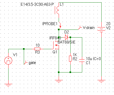
Jay_Diddy_B, D2 is indeed a Schottky - thanks for pointing out that I have the wrong symbol in my library. I'll have to fix that.
Nope, no problems at all. It worked perfectly on the first try. I did "cheat" a bit by double-checking in SPICE where all the critical current paths were, but they were all the obvious ones anyway, so nothing gained from cheating as usual
BravoV, clearly from the pathetic etch job, I've been having a Neanderthal kind of day! The surface is quite chipped, but I don't really care. The inductor was wrapped sparsely enough that it could have been done with bare copper wire anyway. I used cyanoacrylate to reassemble it.
I didn't think of heating the core. It makes sense that it would have an effect, though. Definitely something to experiment with. -
I didn't think of heating the core. It makes sense that it would have an effect, though. Definitely something to experiment with.
The core heating experiment is really useful especially when you have a really tight margin on the core saturation point at your swicher circuit. Highly recommended to try it especially when the circuit might exposed to wide temperature fluctuation range.
For one off project using random ferrite cores or enthusiast like me that love to play with switcher + salvaging inductors, this circuit is a really handy tool to get a unknown inductor saturation profiles.
-
Just ordered my variant of the board at OSH Park, hopefully will get it before Christmas.
-
Looks pretty small, thanks for sharing, can't wait to see the real circuit in work.
Btw, I see you have the trigger output and assuming you have your own modded circuit from the original design maybe ? -
@BravoV, I used your schematic. The only thing I added was a jumper to turn off current limit. I also used compl.pairs instead of single transistors so I won't mix them - there are two distinctive packages. I'm going to try 2N2369A (and 2N2501) in the inverter so also added pads to Q4 to accommodate a TO-18.
The board will be attached directly to the scope's vertical input. -
I can see you're also interested with the experiment to shorten propagation time at the inverting stage, great to hear that, please share the results too.
Fun experiments, cold (normal room temp) vs hot inductor, and the most weirdest effects I found are using magnet on the inductor with various distances to the inductor.
Btw, its not my circuit, credit should goes to Jay_Diddy_B.
-
Here is my build (see pictures). Works very well. Now I need to figure out how to get more current into the inductor (in this circuit current levels at about 20A).
The inductor used in the scope screenshot is secondary winding of Coilcraft DA2032-AL flyback transformer, ~1mH on ferrtite. The sense resistor is 50 mOhm.
-
mazurov,
Congratulations !!
The circuit board looks great. The results you see are the expect results.
Excellent !!
Jay_Diddy_B
-
JDB,
Thank you for designing this!
To all - the PCB can be ordered at OSH Park -> http://oshpark.com/shared_projects/BzgNwX3Y . It seems that Gerbers can also be downloaded from there so if you don't like OSH Park you can fab the board elsewhere. Compl.transistors are FMB3946, all other parts are as per JDB's docs.
Oleg. -
Oleg, thanks for sharing, that is beautifully built & made, it looks so tiny !
Also its cute to see that TO-18 transistor (Is that 2N2369A ?) soldered among that two big caps.
Geezz... 20A is not enough ? Whats the max supply voltage rail for the inductor did you use at that 20 A ? Please keep us updated on your quest for > 20A current setting.
-
First screenshot shows max.current achieved with some pretty large iron powder core inductor at 30V. Second screensot shows what is happening when I increase pulse width. Note that the rep.rate was decreased 10 times since P-FET started melting solder. I can't go past 30V since caps are 35V and they are also quite warm.
The Rsense is 50 mOhm, to get the current multiple the voltage by 20.
I don't know what causes that, seems to be the P-FET. I'll get a bigger one and try again (D2PAK footprints were used here for a reason :-)). It also appears that 2x4700uF bank is an overkill. I'll build another unit capable of higher voltage and try again.
-
About your example here, since it is not clear on the "knee", how do you determine the saturation point ?
Since the 2 x 4700uF are overkill, at what inductor current did you max out ? That 20 A ? (assuming it was max at 30 V)
Keep us updated on your new build, it will be interested to watch.
-
BravoV and the group,
Read this application note from Micrometals: Iron Powder Cores for Switchmode Power Supply Inductors
It can be found here:
http://www.micrometals.com/appnotes_index.html
This will be more than you will ever want to know about inductors
Micrometals is one of the leading manufacturers of powered iron cores.
Jay_Diddy_B
-
About your example here, since it is not clear on the "knee", how do you determine the saturation point ?
The saturation point is where you decide it is.
And as in all electronics, there is no single point, it's always a range/region/area. Some are bigger than others.
It's somewhere between where the curve leaves one asymptote and joins the other asymptote. Take your pick. It all depends on what the application requires.
-
Saturation point is not that interesting by itself. What is interesting is inductance change. When core gets saturated it is not contributing to the inductance anymore , i.e., the inductor becomes "coreless", its inductance decreases (often substantially) and if, for example, this inductor is a part of DC-DC converter, the output ripple will grow.
Ghydda's picture illustrates that. The straight line on the left shows the region where the core is not saturated. From zero current to the point where current curve stops following this line the inductance of the part is the one any old inductance meter will show you. Past this current inductance starts decreasing and the curve will eventually start following the right side straight line when core "disappears".