-
I would stay away from 7 segment displays and any logic IC for counting and 7 seg decoding. I would like to keep everything discrete. Either 10 leds for each player using simple transistors to shift increment the score, or, with the exact same transistor shift increment, provided the output transistors are open-collector and can withstand the HV, send the 10 outputs to nixie tubes for a 0 to 9 count display.
Basically, 1 all transistor circuit, 2 optional displays, 1 LV for leds, of with an HV supply, nice numeric tube display.
What about printing the score on the screen? In an earlier thread on a DIY analog computer, someone (possibly GK?) calculated the patterns needed to print numbers to a scope in a purely analog fashion, so that *could* be used, though I'm not sure how complex the implementation would be.
Failing that you could do a pair of discrete resistor ladder DACs for X and Y; the data for drawing the numbers would come from a ROM (you could use an array of diodes in place of the ROM to stay discrete), then just raster scan them out during a multiplexing time slot. That's how Tektronix did readouts on their CRT based scopes. -
For basic through-hole home-brew stuff I use a 50/100 thou grid. Small-signal component leads get big 80 thou. dia. pads with 32 thou (0.8mm) dia. holes exclusively. This makes for easy manual manufacture still allows a decent packing density. 671 individual components on this 150mm x 300mm board (from another project that I am steadily beavering away at behind the scenes......):
-
I would stay away from 7 segment displays and any logic IC for counting and 7 seg decoding. I would like to keep everything discrete. Either 10 leds for each player using simple transistors to shift increment the score, or, with the exact same transistor shift increment, provided the output transistors are open-collector and can withstand the HV, send the 10 outputs to nixie tubes for a 0 to 9 count display.
Basically, 1 all transistor circuit, 2 optional displays, 1 LV for leds, of with an HV supply, nice numeric tube display.
What about printing the score on the screen? In an earlier thread on a DIY analog computer, someone (possibly GK?) calculated the patterns needed to print numbers to a scope in a purely analog fashion, so that *could* be used, though I'm not sure how complex the implementation would be.
Failing that you could do a pair of discrete resistor ladder DACs for X and Y; the data for drawing the numbers would come from a ROM (you could use an array of diodes in place of the ROM to stay discrete), then just raster scan them out during a multiplexing time slot. That's how Tektronix did readouts on their CRT based scopes.
But you've just ~doubled the complexity of the project. If you want to accommodate that as an optional add-on the current multiplexer logic will have to be scrapped and majorly redesigned for a start. I say just stick to the current specification.
Also, yes, that was me in the analog computing thread where development of my "Fourier synthesis character generator" was documented:
http://www.glensstuff.com/fouriersynthchargen/fouriersynthchargen.htm
-
I would stay away from 7 segment displays and any logic IC for counting and 7 seg decoding. I would like to keep everything discrete. Either 10 leds for each player using simple transistors to shift increment the score, or, with the exact same transistor shift increment, provided the output transistors are open-collector and can withstand the HV, send the 10 outputs to nixie tubes for a 0 to 9 count display.
Basically, 1 all transistor circuit, 2 optional displays, 1 LV for leds, of with an HV supply, nice numeric tube display.
What about printing the score on the screen? In an earlier thread on a DIY analog computer, someone (possibly GK?) calculated the patterns needed to print numbers to a scope in a purely analog fashion, so that *could* be used, though I'm not sure how complex the implementation would be.
Failing that you could do a pair of discrete resistor ladder DACs for X and Y; the data for drawing the numbers would come from a ROM (you could use an array of diodes in place of the ROM to stay discrete), then just raster scan them out during a multiplexing time slot. That's how Tektronix did readouts on their CRT based scopes.
But you've just ~doubled the complexity of the project. If you want to accommodate that as an optional add-on the current multiplexer logic will have to be scrapped and majorly redesigned. I say just stick to the current specification.
Also, yes, that was me in the analog computing thread where development of my "Fourier synthesis character generator" was documented:
http://www.glensstuff.com/fouriersynthchargen/fouriersynthchargen.htm
Yeah, I concur it would majorly up the complexity. I just thought I'd throw it out there.
Personally, I think using some of those cute HP bubble 7-seg displays or even just a row of individual LEDs would be the way to go. -
Yeah, just route the "End match" and "Paddle hit" lines to a header. That will permit an off-screen scoring counter to be added as an option without any modification to the design, implemented however who is making and adding it fancies.
-
Continuing with the documentation........... Here is the equivalent diagram of a rather simple section of the game - the Velocity Integrator. The Velocity Integrator provides the complementary potentials, +velocity and -velocity, which are in turn integrated by the Ball Horizontal and Ball Vertical Movement circuits, and thus determine the speed at which the ball moves across the screen.
The potential across the timing capacitor Cv is initially held at 0V courtesy of the (open collector) discharge line. When the ball is served and a match begins the discharge line is released and Cv begins a linear charge towards the positive supply rail. An initial offset potential of approx 0.6V (courtesy of a transistor Vbe-drop in the timing capacitors buffer circuit) provides the initial velocity, or speed at which the ball begins to move the instant it is served.
-
Equiv. diagram for the Ball Horizontal Movement circuit:
-
Might as well mention it; The other night in a fit of immodesty for the first time I tipped a personal project for the Hackaday blog!
"Every scrap of it is circuits of his own design, executed dead bug style, apparently because [GK] enjoys life on hard mode."
-
Enlarge all the pads hole to at least 0.8, especially C2.Tim, great work, if you're fussy about layouts they do take some real time.
May I ask what size annular ring size you're using and the pad hole size ?
I've had some pads lift when reworking PCB's and as a result my preference is for larger pads to minimize the chance of this.
When I can I stick with 100 mil and maybe alter the shape from round if more clearances are needed.
As promised: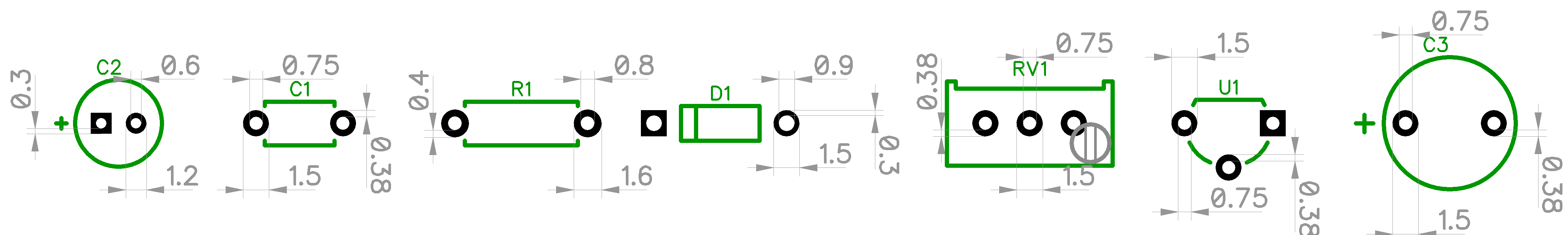
http://timb.us/PDF/Scope_Pong_Pad_Sizes.pdf
Enlarge all the pad outer diameters to 1.6, and make C3's pad size 1.8.
Remember, home build PCBs usually are drilled with 1 drill size for as much of the PCB as possible as we may be working with something like a mini Dremel drill press.
For the 1N400x diodes, make the holes 1mm, pads 2mm.
-
Thanks Tim, check GK's comments, they somewhat align with mine that your annular rings could be a tad larger.Tim, great work, if you're fussy about layouts they do take some real time.
May I ask what size annular ring size you're using and the pad hole size ?
I've had some pads lift when reworking PCB's and as a result my preference is for larger pads to minimize the chance of this.
When I can I stick with 100 mil and maybe alter the shape from round if more clearances are needed.
As promised:
http://timb.us/PDF/Scope_Pong_Pad_Sizes.pdf
He suggests 80 mil which is 2 mm. Hole sizing looks great. -
Ummm, I go about it the other way, drill everything at 0.6 mm and then enlarge those that need to be bigger.
Enlarge all the pads hole to at least 0.8, especially C2.Tim, great work, if you're fussy about layouts they do take some real time.
May I ask what size annular ring size you're using and the pad hole size ?
I've had some pads lift when reworking PCB's and as a result my preference is for larger pads to minimize the chance of this.
When I can I stick with 100 mil and maybe alter the shape from round if more clearances are needed.
As promised:
http://timb.us/PDF/Scope_Pong_Pad_Sizes.pdf
Enlarge all the pad outer diameters to 1.6, and make C3's pad size 1.8.
Remember, home build PCBs usually are drilled with 1 drill size for as much of the PCB as possible as we may be working with something like a mini Dremel drill press.
For the 1N400x diodes, make the holes 1mm, pads 2mm.
I set hole size for everything at 20 mil (0.5 mm) which then helps center the drill bit in the pad, but I use paxolin PCB like GK that is much kinder on bits and you can successfully use HHS bits and not need tungsten. -
Yes, having a smaller hole does add more copper contact and working with 1 smaller bit is easier. I agree, 0.6mm would be good, however, if you have a professional PCB made, you can't re-drill these without a mess. I tried to select a values to make any type of manufacturing choice happy.
On this PCB, only the terminal block connectors and the 1N400x diodes will probably need to be drilled a second time to the larger required size. The larger electrolytic caps and sip rail as well... For drill, 0.8mm for the mass majority of everything else should be ok.
-
Enlarge all the pads hole to at least 0.8, especially C2.Tim, great work, if you're fussy about layouts they do take some real time.
May I ask what size annular ring size you're using and the pad hole size ?
I've had some pads lift when reworking PCB's and as a result my preference is for larger pads to minimize the chance of this.
When I can I stick with 100 mil and maybe alter the shape from round if more clearances are needed.
As promised:
http://timb.us/PDF/Scope_Pong_Pad_Sizes.pdf
Enlarge all the pad outer diameters to 1.6, and make C3's pad size 1.8.
Remember, home build PCBs usually are drilled with 1 drill size for as much of the PCB as possible as we may be working with something like a mini Dremel drill press.
For the 1N400x diodes, make the holes 1mm, pads 2mm.
Earlier someone said go with 30mil if I can, 20 mil minimum, so that's what I did. I will enlarge the DO-31 rings as I agree, they're too small.
How about this: What if I did everything 0.75mm/1.5mm, except C3 and D1? I could do those 1mm/2mm. Since a lot of the patterns are already 0.75/1.5mm, I wouldn't have to go back and move most of the stuff I've already put down.
If the extra 0.05mm is that critical, I'll do it, otherwise it would save me a lot of extra work at this point.
Edit: By move stuff, I mean that in some areas, I've routed traces just close enough to pads so that it doesn't break the ground pour with the current pad sizes. If I upped all the transistors to 0.8/1.6, I'd have to go back and reroute a lot of stuff. I can do it, I don't mind, but if the 0.05mm isn't *that* critical, I'd rather spend the time routing new sections. -
You may be fine with all the pads and holes Tim, it's just one of my pet hates, annular rings too small.
I'm somewhat thinking of those that will be buying PCB's or using your files to etch their own PCB. Those that have done some PCB work will have no problem with your work I don't think, moreso those with limited experience taking on this as their first big project. If it's populated without mistake and zero components need to be reworked, then I don't see any problems.
After the effort I know you're putting into this I wouldn't want to see criticism of your efforts by those that have taken on something more complex than they should've.
It's a heap of work Tim, you and GK decide what the outcome should be. -
You may be fine with all the pads and holes Tim, it's just one of my pet hates, annular rings too small.
I'm somewhat thinking of those that will be buying PCB's or using your files to etch their own PCB. Those that have done some PCB work will have no problem with your work I don't think, moreso those with limited experience taking on this as their first big project. If it's populated without mistake and zero components need to be reworked, then I don't see any problems.
After the effort I know you're putting into this I wouldn't want to see criticism of your efforts by those that have taken on something more complex than they should've.
It's a heap of work Tim, you and GK decide what the outcome should be.
Yeah, I agree with the hate for small annular rings! The diode pattern really needs bigger rings and it's something I forgot to go back and fix. (I copied the DipTrace pattern for the DO-31 package and simply changed the pad spacing without fixing the pad sizes.)
For C2, I had the pad/holes larger, but I felt they were too close together, so made them a bit smaller. In reality, they need to be 0.75/1.5, so I'll go back and fix that. (Lead diameter for the caps is 0.5 +-0.1, so after accounting for hole plating on a professional board, it really needs to be 0.75mm minimum.)
I went with 2mm caps for the 10uF parts as they're at least easy to obtain; 1.5mm is starting to be more common, but the pad spacing would have been absolutely tiny!
I'll make some changes tonight and post another picture of the pad/hole sizes for you guys. I want to do this right, so if 0.8 vs 0.75 will really make a difference, I don't mind going back and changing stuff I've already laid out. Like I said, if the extra 0.05mm isn't that big of a deal, my time could be spent elsewhere. I'll defer to you guys, the much more experienced DIY board makers, on that.
I haven't hand etched and drilled a board in close to 20 years, so I appreciate all the advice and tips from everyone on making this home etchable. I should pickup some supplies and try to etch a few smaller TH boards myself, to get a feel for the process. (The last board I did, I was in my early teens and used a Sharpie and some of those rub down traces and holes, with an etching kit from Radio Shack!)
Edit: When I originally did the patterns, I did it with the intent that most people would buy a professionally made PCB (at $15 for two boards it seems like a bargain), however I made sure the holes were at least 20mil and optimally closer to 30mil, per one of your recommendations. I didn't think about having to change drill bit sizes, so I can see how having as many of the holes as possible one size would be advantageous. -
Considering the size and number of holes you'd be pretty nuts to home-brew a PCB like this. For something like this, the last thing you need is the additional hassle of tracking down shorts & broken tracks.
It also adds some constraints on the design - e.g. not using top connections to parts that can't be top-side soldered, like multiturn trimmers & connectors.
A PTH board will be a lot more robust, and it's so cheap now, especially as I suspect enough people would be interested to do a small group order, that it's probably not worth going too overboard making the design optimised for homebrew PCBs.
That being said there's never any harm in making track widths & gaps as wide as practical, as this also increases yield on production boards and improves reworkability.
-
It also adds some constraints on the design - e.g. not using top connections to parts that can't be top-side soldered, like multiturn trimmers & connectors.
These 2 parts in the design are not too terrible a constraint. It's the reason for making all the other footprint solder-able on both sides and using the TO-92 footprint with the off-center pin #2.
Home etched can be of quality and PCB milling machined boards I can have done locally for 5$, there wont be shorts or breaks, but you still need to solder on both sides.
-
Okay boys and girls (if there are any girls), I have finally finished all of the equivalent diagrams and amended circuit diagrams and have collated them into a single 25 page (21 Mb) PDF document. Here it is:
http://www.glensstuff.com/pong/Oscilloscope_Pong.pdf
-
Okay, so I didn't get nearly as much done as I planned tonight, feeling a bit under the weather so I decided to make an early night of it.
I finished the Function Generator section, but forgot to upload the PDF/images for them, doh!
I also did the Multiplexer FET Gate Drive section; I implemented it as a sub-section of the Multiplexer Logic; the Horizontal and Vertical section will be placed directly above the Multiplexer section. That way the X, Y and Z BNC connectors will all be facing the same side on one board.
I also added some test points and cleaned up some traces in the Multiplexer Logic section.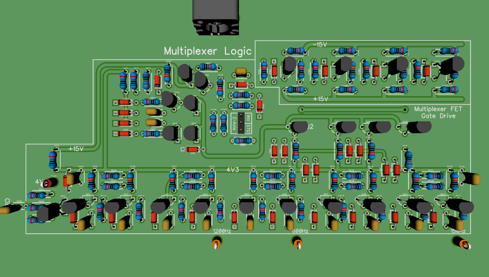
http://timb.us/PDF/Scope_Pong_Multiplexer_Logic_FET_Drive.pdf -
Okay boys and girls (if there are any girls), I have finally finished all of the equivalent diagrams and amended circuit diagrams and have collated them into a single 25 page (21 Mb) PDF document. Here it is:
http://www.glensstuff.com/pong/Oscilloscope_Pong.pdf
Sweet! Nice work.Considering the size and number of holes you'd be pretty nuts to home-brew a PCB like this. For something like this, the last thing you need is the additional hassle of tracking down shorts & broken tracks.
It also adds some constraints on the design - e.g. not using top connections to parts that can't be top-side soldered, like multiturn trimmers & connectors.
A PTH board will be a lot more robust, and it's so cheap now, especially as I suspect enough people would be interested to do a small group order, that it's probably not worth going too overboard making the design optimised for homebrew PCBs.
That being said there's never any harm in making track widths & gaps as wide as practical, as this also increases yield on production boards and improves reworkability.
Once I finish the board, my plan was to do a group order that includes the boards and all parts (over 700 of them, per kit) which should significantly bring the price down. Based on the response to my initial inquiries, I think most people will go this route, but there were a few people who wanted to etch their own boards, so I'm trying to to at least make it possible.
-
First of all can I say what a great thread this is. I always follow GK's projects, and this time around I should be able to build it too thanks to the group effort here.
I've been thinking (a little) about the discussion on adding scorekeeping to the game.
I like GK's all discrete analog construction, so I'm in the camp that thinks 7 segment displays or LEDs would be out of place here.
So, we already have a scope as the court, how about using a meter or two to display the score? Let's bring more test equipment into the game!
Some possibilities:
Two volt meters, one per player, 1v per point.
A volt meter that reads +ve or -ve depending on the player, 1v per point. Would show the running points difference.
One volt meter, but with different voltage increments per player, so for example 3.5v would be a score of 3 to 5.
Exchange volt meters for frequency counters or totalisers?
I'll defer to GK to assess the complexity, but hopefully the two volt meter option would be straightforward - perhaps just a couple of integrators? -
Thinking about how you could add an option connector to add onscreen scoring.
If the design just included some dead-time in the display cycle, and a way to switch the outputs to the option connector during that time, that would allow for an external renderer. The switch-over/mux could be on the option board, and jumpered out when not fitted.
-
I like GK's all discrete analog construction, so I'm in the camp that thinks 7 segment displays or LEDs would be out of place here.
Well, LEDs are still discrete. You could even make a 7-segment display with discrete LEDs if you really wanted (though I think some of those little HP bubble 7-segment displays wouldn't look out of place, and they *are* period appropriate).
It isn't all analog, either. Sure, the graphics are drawn though a combination of sine, cosine, triangle and square waves generated by discrete integrators and op-amps, but that's not the end of the story... It's also full of discrete digital components as well; flip-flops, logic gates, inverters and latches! There are also comparators, which are half-digital (kind of). In fact, I'd say at least half of the circuits are digital in nature.
So, personally, I don't see where a discrete counter circuit that outputs to a period appropriate LED display would be out of place. In fact, I think it could kind of balance out the "other side" of the underlying circuits. That is, you'd have an analog (the scope) and digital (the LEDs) output for a project that's already both analog and digital!
Just my two cents, anyway. -
Okay, so I didn't get nearly as much done as I planned tonight, feeling a bit under the weather so I decided to make an early night of it.
I finished the Function Generator section, but forgot to upload the PDF/images for them, doh!
I also did the Multiplexer FET Gate Drive section; I implemented it as a sub-section of the Multiplexer Logic; the Horizontal and Vertical section will be placed directly above the Multiplexer section. That way the X, Y and Z BNC connectors will all be facing the same side on one board.
I also added some test points and cleaned up some traces in the Multiplexer Logic section.
Hi Tim. You're making some good progress, but there are some important layout points I should probably interject here with. In the gate drive circuit there is associated with each JFET pair a 20k resistor terminating the gate terminals to ground and a commutation diode. In your schematic these are R1101, R1105, R1109, R1113, D1101, D1102, D1103 and D1104.
When a JFET pair is turned ON its respective commutation diode is reverse biased and the gates are effectively isolated and terminated to ground through the respective 20k resistor. We don't want this termination resistor to be half a board width away with a long inductive track in between. And although the discrete op-amps in the horizontal and vertical deflection circuit do not have a super high GBWP, it is still good practice to minimize the virtual earth nets.
These requirement make it necessary to bunch up to some degree the JFETs and their associated gate diodes and resistors around the inverting inputs of the respective op-amps. Attached is a scribble of a quick/rough diagram approximating an acceptable layout that meets these requirements.
The length of the logic-level digital control lines emanating from the cathodes of the gate commutation diodes really doesn't matter; it's just these components that you have to keep reasonably compact.
-
In addition to the above I should have also mentioned that the input resistors which connect directly to the JFET drains should be placed as close to the JFETs as practical.