-
No, you need to generate wait states.
You could build it and try out with a Z80 clock speed of 4MHz - if that works you can go back to 8MHz and see what happens.
Wait states? Something new to learn about there!
Okay, so you're suggesting before I get too wrapped up in timings I should confirm it all works at 4MHz then try it at 8 as there's a chance it could still work and either way would save me a lot of hassle by not jumping the gun? I really need to change my methodology as I'm in too much of a rush to get it working all the time!
The only consideration I can think of is that the serial comms speed will need to be halved if I do that, otherwise it should be pretty straightforward, I'm hoping?
Will let you know how it goes!
We have seen with some of Grant's designs that he has run older peripheral chips much faster than their design speeds but has got away with it - so you might be lucky.
That said you should probably budget a couple of 74xx74's and a couple of gates to generate the wait states if necessary.
Or drive the whole thing from a Z80 PIO and bit-bang the control signals. -
OK.
The following will add two wait states to any I/O cycle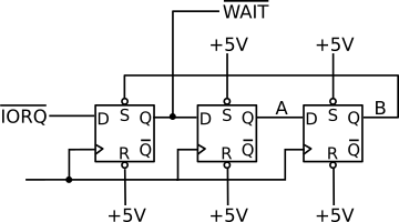
It is based on the circuit in the Z80 user manual for adding wait states to the M1 cycle - but with an extra 1 clock cycle delay before de-asserting \$\small\overline{WAIT}\$. I'm not sure if it is possible to do two wait states with just two flip-flops.
The timing is as follows, TW0 is the automatically inserted wait state generated by the CPU TW1 and TW2 are the two additional wait states.
EDIT: Oops, the 2nd "T1" should, obviously, be "T2"
This stretches the active length of the I/O cycle with an 8MHz CPU clock to about 550ns - which should be fine for the AY-3-8912.
If you don't want to slow all I/O cycles use a select signal generated from \$\small\overline{IORQ}\$ and relevant address lines rather than just \$\small\overline{IORQ}\$ as input to the 1st flip-flop. -
This stretches the active length of the I/O cycle with an 8MHz CPU clock to about 550ns - which should be fine for the AY-3-8912.
If you don't want to slow all I/O cycles use a select signal generated from \$\small\overline{IORQ}\$ and relevant address lines rather than just \$\small\overline{IORQ}\$ as input to the 1st flip-flop.
Wow, thanks grumpydoc, that's awesome!
I've just written a test routine in my monitor ROM code to write a value to the PSG IO port and read it back. I've yet to burn it to the ROM and test it, but I'm guessing it'll be a quick test (without writing the routines to play sounds) to see if the AY-3-8912 can handle 8MHz. If not, I'll run the SBC clock through a divide-by-2 flip-flop to drop the clock under 4MHz (it'll be 3.62..blah MHz instead, but the pulse widths should be fully compatible with the PSG then.) If and when it works at that speed, I'll get to work on your wait-state solution and bump the clock speed back up to 8MHz.
Out of interest, are there any more modern versions/alternatives of the AY-3-891x PSG chip? -
Hmm, okay, it seems that it doesn't like 8MHz - no surprises there, really. I've tried reading and writing to the IO port on the 8912, but it's not playing. If I read Port A I'm getting FF or 00, seemingly randomly, as values no matter whether I ground one of the IO pins or not. Writing to the IO port after setting it up as an output also seems to have no effect - the pins are all high irrespective of what values I write to the port.
Just for info (and in case I'm making an error in the way I'm accessing the PSG), below is the code I've written to test reading/writing to the IO port:Code: [Select]CPSGOUT:
POP HL ; Get command line pointer
CALL GETBYTE ; Get 1-byte value from command line into E
LD HL,AYPWRITE ; Display the port write text
CALL MPRINT
LD A,E ; Load value into A
CALL PHEX ; Display it as a hexadecimal
LD A,'H' ; ...with an 'H' on the end
CALL TXA
; Set IOA to OUTPUT
LD A,07H ; Select address R7 (ENABLE register)
OUT (AY_LATCH),A ; Latch address R7
LD A,40H ;
OUT (AY_WRITE),A ; Set R7 to 40H (IOA set to output - bit 6 HIGH)
; Set value in IOA
LD A,0FH ; Load A with Register 16 (IO Port A)
OUT (AY_LATCH),A ; Latch Register 16 in PSG
LD A,E ; Load A with value from GETBYTE
OUT (AY_WRITE),A ; Write value to PSG
JP COMMAND ; Return to Direct Mode CLI
CPSGIN:
POP HL ; Dump command line pointer
LD HL,AYPREAD ; Display read text
CALL MPRINT
; Set IOA to INPUT
LD A,07H ; Select address R7 (ENABLE register)
OUT (AY_LATCH),A ; Latch address R7
LD A,0
OUT (AY_WRITE),A ; Set R7 to 0 (IOA set to input - bit 6 LOW)
; Read IOA
LD A,0FH ; Load A with Register 16
OUT (AY_LATCH),A ; Latch Register 16 in PSG
IN A,(AY_READ) ; Read register R15
CALL PHEX
LD A,'H'
CALL TXA
JP COMMAND ; Return to Direct Mode CLI -
After a little more playing around and dropping the SBC's clock to 3.6864 MHz, changing the BC2 input from just an inverted Y1 to Y1 AND IORQ to reduce false activations of the PSG and re-writing the IO routines slightly (IOA is 0Eh, or register 15 not 0Fh, register 16) I have managed to get some values read from IOA that match up to what I've set up on the breadboard.
Here's the rewritten code I'm using:Code: [Select]CPSGOUT:
POP HL ; Get command line pointer
CALL GETBYTE ; Get 1-byte value from command line
LD HL,AYPWRITE ; Display the port write text
CALL MPRINT
LD A,E ; Load value into A
CALL PHEX ; Display it...
LD A,'h' ; ...with an 'H' on the end
CALL TXA
; Set IOA to OUTPUT
LD A,$07 ; Select address R7 (select ENABLE register)
OUT (AY_LATCH),A ; Latch address R7
LD A,40H ;
OUT (AY_WRITE),A ; Set R7 to 40H (IOA set to output)
; Set value in IOA
LD A,0EH ; Load A with Register 16
OUT (AY_LATCH),A ; Latch Register 16 in PSG
LD A,E ; Load A with value
OUT (AY_WRITE),A ; Write value to PSG
JP COMMAND ; Return to Direct Mode CLI
CPSGIN:
POP HL ; Dump command line pointer
LD HL,AYPREAD ; Display read text
CALL MPRINT
; Set IOA to INPUT
LD A,$07 ; Select address R7 (select ENABLE register)
OUT (AY_LATCH),A ; Latch address R7
LD A,0
OUT (AY_WRITE),A ; Set R7 to 0 (IOA set to input)
; Read IOA
LD A,0EH ; Load A with Register 16
OUT (AY_LATCH),A ; Latch Register 16 in PSG
IN A,(AY_READ) ; Read register R15
CALL PHEX
LD A,'h'
CALL TXA
JP COMMAND ; Return to Direct Mode CLI
So it seems reading IOA is working, albeit not quite 100% of the time (sometimes I just get FF returned instead of a smaller value determined by the grounding resistors I've placed on the IO pins).
Setting IOA to output and sending a value to it doesn't seem to be doing anything - so I'd appreciate some comments from anyone who knows anything about interfacing an AY-3-8912 to the Z80. All the IO pins seem to be high, no matter what value I send to the IO port. I'm wondering if I'm using the wrong value (40h) to send to Register 7 - it should be specifying bit 6 high to set IOA into an output state, but I'm not sure that's happening, or even if 07h is the right address to latch to set the enable values in register 7....? -
Can you post the exact arrangement for driving BDIR, BC1, BC2 and A8/9 if applicable?
-
Can you post the exact arrangement for driving BDIR, BC1, BC2 and A8/9 if applicable?
Sure.. see below:
First, the image above shows the '138 setup (IO addressing) on the SBC as per Grant's CP/M schematic. My SBC IO is identical to Grant's schematic. I'm using Y1 on the '138 to control chip select on the AY-3-8912 (via pin BC2) - this equates to an IO address range of 08h-0Fh, if my calculations are correct.
Next - the PSG circuit (focusing on the SBC interface):
Above is a closeup of the interface for the PSG. As you can see, BC1 is driven by A1, BDIR by A0, and BC2 (which should be HIGH for the PSG to do anything) is driven from an inverted signal from ~IORQ and ~Y1.
This should, if I'm right (a big if I know!), give me the following addresses for the following commands:
So, to write to the PSG, I'd use OUT (09H),value. Address 09 is within the IO range of the PSG (being 08-0F), so Y1 will go low (which is high after the inverter) and BDIR will go high as it's driven by A0, providing the WRITE command to the PSG.
That's the plan, anyway...
-
OK, so BC2 will be low unless both \$\small\overline{IORQ}\$ and \$\small\overline{Y1}\$ are low - that's fine.
But BC1 and BDIR are just driven from A0 and A1, lets have a look at the command table in the manual:BDIR BC2 BC1 0 0 0 Inactive 0 0 1 Latch address 0 1 0 Inactive 0 1 1 Read 1 0 0 Latch address 1 0 1 Inactive 1 1 0 Write 1 1 1 Latch address
Just concentrate on the entries with BC2 = 0BDIR BC2 BC1 0 0 0 Inactive 0 0 1 Latch address 1 0 0 Latch address 1 0 1 Inactive
As you can see even when BC2 is low you can latch an address, in fact any time A0 != A1 - so there's a good chance that the LD A after the write that you intended to latch the address for the register will cause a different address to be latched. There are three opportunities for doing so - the M1 cycle of the LD, the refresh, and the read of the operand - in fact either the M1 or the opcode read is guaranteed to have A0 != A1 and the refresh will have that pattern two cycles out of four. And if that instruction doesn't mung things it will probably happen (again) as you read the opcode for the OUT and then as you read the operand for the port number.
You need to make sure that an inactive combination is presented on BDIR, BC1 and BC2 any time the AY-3-8912 is not selected. I think I suggested as way of doing that a couple of posts back.
EDIT - I did but I got it wrong, it should have been
BC2 and A8 should be tied high.
If the select ( \$\small\overline{IORQ}\$ + \$\small\overline{Y1}\$ in your case) is active low then when inactive (high) it will force BC1 and BDIR low, i.e when the chip is not selected.
For some reason I drew it out for an active high select then wrote an active low one in
-
 I overlooked my inexperience with this stuff and didn't think of the obvious - that the PSG was being latched/read/written to inadvertently by the ungated A0 and A1 lines!
Thanks grumpdoc, as usual you're spot on.
Question though regarding the proposed solution - given my existing setup, would it be sufficient to take the inverted input to BC2 and connect that to A8, and instead pull BC2 high by connecting to Vcc?
That way, A8 will be held low all the time the PSG isn't being accessed (and, if I've read the manual right, should effectively disable the PSG). When the CPU wants to latch, read or write the PSG's registers, A8 will go high and the PSG will be available (as BC2 is permanently held high), leaving A0 and A1 to select the correct function through the BC1 and BDIR pins...?
That way I can save adding any extra logic chips and just swap a couple of wires...
EDIT: Hmm... no, that appears not to be working either.
-
Question though regarding the proposed solution - given my existing setup, would it be sufficient to take the inverted input to BC2 and connect that to A8, and instead pull BC2 high by connecting to Vcc?
I was going to say give it a go
That way, A8 will be held low all the time the PSG isn't being accessed (and, if I've read the manual right, should effectively disable the PSG). When the CPU wants to latch, read or write the PSG's registers, A8 will go high and the PSG will be available (as BC2 is permanently held high), leaving A0 and A1 to select the correct function through the BC1 and BDIR pins...?
That way I can save adding any extra logic chips and just swap a couple of wires...
EDIT: Hmm... no, that appears not to be working either.
The way I read the datasheet it wasn't completely clear that having A8 low deactivated the chip, rather than just the data bus buffers.
Edit: Though I suppose it should given the intended CPU interfacing. However to be certain I'd make sure that BDIR/BC1/BC2 are forced inactive when you don't want to talk to the chip.
-
I was going to say give it a go
The way I read the datasheet it wasn't completely clear that having A8 low deactivated the chip, rather than just the data bus buffers.
Edit: Though I suppose it should given the intended CPU interfacing. However to be certain I'd make sure that BDIR/BC1/BC2 are forced inactive when you don't want to talk to the chip.
I don't seem to be getting any consistency in the results or even results that I would expect. With the change I made in my last post, I'd have thought the IO from the chip would at least be predictable - having A8 low should make the buffers inactive and thus prevent any miscellaneous signals from reading/writing or latching the PSG unintentionally. Instead, I'm just getting 00 as a result from the IO port.
It doesn't help that I'm not sure which IO register I should be addressing... According to the datasheet, Registers R16 and R17 control IOA and IOB. I'm using an 8912 which only has IOA, so R16 is the logical register for addressing the IO port, which should be 0F. However, I've read elsewhere http://forum.6502.org/viewtopic.php?f=4&t=3339&sid=9ab9958abd00ad39541ab00a72050380&start=15 that the registers should be dropped by 02 - so R16 for IOA becomes 0D??
So I should do the following to read from IOA:Code: [Select]LD A,$07 ; Select address R7 (select ENABLE register)
OUT (AY_LATCH),A ; Latch address R7
LD A,0
OUT (AY_WRITE),A ; Set R7 to 0 (IOA set to input)
; Read IOA
OUT (AY_LATCH),0DH ; Latch Register 14 in PSG
IN A,(AY_READ) ; Read register R14
But that is just returning 00 as well. (I'm reading a value from memory for the IO register, so I can just POKE 0D, 0F, or whatever to that location and when I read the IO port it gets that value and uses it as the register to latch, making testing different register values much quicker.) I can't seem to replicate my results yesterday when I was (albeit not totally reliably) able to get values from the IO port.
I'm running the clock through a flipflop configured as a clock divider, which is halving the SBC clock from 3.68 MHz down to 1.84 MHz, well within the stated 1-2 MHz clockspeed for the PSG. The audio circuit is circumstantial as I'm testing the PSG's IO first. The PSG is otherwise a simple data bus connection to the SBC and control signals for BC1, BC2 and BDIR. I'm hoping it's just very particular about how those control signals are managed.
I'm going to implement your suggestion, grumpydoc and see if that works. -
Okay, this is how I've interpreted your solution, grumpydoc - I hope it's correct. Ironically, if I'm reading your solution properly, it means I can drop the inverter and replace it with the NOR gate, so the chip count remains the same.

Is this what you're suggesting? So long as ~Y1 and ~IORQ remain high, BC1 and BDIR will be low. But when the PSG is being accessed, ~Y1 and ~IORQ will go low, allowing either (or both) A0 and A1 to pass a high through to the PSG to read/write/latch as appropriate - am I right?
-
I'd drive BDIR from \$\small\overline{WR}\$ but I don't see why driving it from A0 would not work.
-
Am I messing something or are you?
Grant's 138 is just address decode. So any time Y1's address range appears on bus then Y1 goes low. This could be anything and includes the time from one address changing to a different address.
Y1 output is noise or garbage.
This only becomes valid when gated with more signals.
Each IO access to AY-3-8912 must have two of three signals valid low to be a valid IO read or IO write..
IORQ & RD is one and IORQ & WR is second.
IORQ by it's self is not enough as IORQ goes low at other times then just IO read & write.
Now think about what is happening now!
What is keeping two things from responding when RD is low and only one device on data bus should be active?
Is the AY-3-8912 being told to drive the data bus for a memory read of ??08H to ??0FH?
Even this is not correct because only IOWR is used.
So AY-3-8912 drives data bus any time IOWR is high and ??08H to ??0FH is on address bus.
I see no use of RD in access of AY-3-8912.
Grant creates two signals that must be used if you are not using the Z80 signals directly. IORD & IOWR
I see you needing to use 138 Y1 low AND ( IORD low OR IOWR low ) as a chip select signal.
A0 should be used to select between the two data bus ports on AY-3-8912
You have a read & write data port.
You have a write address port with read address port not used.
Okay, this is how I've interpreted your solution, grumpydoc - I hope it's correct. Ironically, if I'm reading your solution properly, it means I can drop the inverter and replace it with the NOR gate, so the chip count remains the same.
Is this what you're suggesting? So long as ~Y1 and ~IORQ remain high, BC1 and BDIR will be low. But when the PSG is being accessed, ~Y1 and ~IORQ will go low, allowing either (or both) A0 and A1 to pass a high through to the PSG to read/write/latch as appropriate - am I right?
Here you are not using RD or WR, so what address is used sets data bus direction of PSG.
You would look at all states of Z80 to verify that when PSG is driving bus nothing else will.
When is data bus written to PSG?
A low to high of WR is the Z80 normal transition. Here you have IORQ going high as a PSG write transition and end of PSG read. Again timing matters and needs to be checked -
A low to high of WR is the Z80 normal transition. Here you have IORQ going high as a PSG write transition and end of PSG read. Again timing matters and needs to be checked
Using A0 to drive the bus direction is unusual, certainly, and I would choose to use WR as I have said a couple of times but it would actually work - as long as one address is always used for read and one for write.QuoteIORQ by it's self is not enough as IORQ goes low at other times then just IO read & write.
Ah, yes - I was forgetting something myself. IORQ is active with M1 to indicate an interrupt acknowledge so, yes, you are right as it stands there can still be problems. I get so used to running IORQ and M1 into the enable pins on I/O decode that I didn't think about this - Grant's design does not do so and you need to make sure that the select is not active if M1 is low. -
Ah, yes - I was forgetting something myself. IORQ is active with M1 to indicate an interrupt acknowledge so, yes, you are right as it stands there can still be problems. I get so used to running IORQ and M1 into the enable pins on I/O decode that I didn't think about this - Grant's design does not do so and you need to make sure that the select is not active if M1 is low.
I was wondering if something else was going on, but don't know enough about the system to have spotted it. One question I have about Grant's I/O decode design though - and it's been bugging me since I moved from the v1 (non-CP/M) SBC to the v2 one - and that's why doesn't he have IORQ and M1 going to the enable pins on the '138?
Anyhow - the SIO/2 is interrupt driven on the Rx side, so that's likely causing problems with the interrupt causing chaos with the PSG. So, another gate is required for the PSG select signal (currently ~Y1 and ~IORQ) to ensure the PSG is not active when M1 is low? -
Using A0 to drive the bus direction is unusual, certainly, and I would choose to use WR as I have said a couple of times but it would actually work - as long as one address is always used for read and one for write.
I only went with using A0 and A1 as it was the first solution that sprang to mind with needing to be able to read, write AND latch using only 2 lines. If there's benefits to using ~WR instead of A1 (presumably) then let me know and I'll change the design - it's only a few equates I need to change in the assembly.
-
Ah, yes - I was forgetting something myself. IORQ is active with M1 to indicate an interrupt acknowledge so, yes, you are right as it stands there can still be problems. I get so used to running IORQ and M1 into the enable pins on I/O decode that I didn't think about this - Grant's design does not do so and you need to make sure that the select is not active if M1 is low.
I was wondering if something else was going on, but don't know enough about the system to have spotted it. One question I have about Grant's I/O decode design though - and it's been bugging me since I moved from the v1 (non-CP/M) SBC to the v2 one - and that's why doesn't he have IORQ and M1 going to the enable pins on the '138?
Anyhow - the SIO/2 is interrupt driven on the Rx side, so that's likely causing problems with the interrupt causing chaos with the PSG. So, another gate is required for the PSG select signal (currently ~Y1 and ~IORQ) to ensure the PSG is not active when M1 is low?
There is a lot about Grant's design I do not care for.
When using 374's for IO the common practice is to have two 138's used. One would have RD as final signal to enable 138 outputs, while other uses WR.
In front of this would be an additional 138. Timing then determines where IORQ is connected. Connected to first two is great as you have most time for a stable address.
But if you are using chips like SIO, it can be better to connect IORQ to the last 138.
So first two 138's gives you 8 input & output ports jusing A0-A2
Third 138 uses 3 more address lines A3-A5
Now if you look at 139, you see a dual 1 of 4 so 1 139 can give you 4 IO read write ports. This matches better with chips like SIO that need two address lines and makes using some SIO,PIO and others along with ports based on 374's
The above is built to expand while working with the Z80.
There are good reasons to have separate WR & RD signals like Z80 uses compared to one signal like some CPU's use. One problem is when is the combined RD/WR valid. With separate signals valid & signal are one.
Like I said
use IORQ & RD for IO Read
use IORQ & WR for IO Write.
and you will not need to worry about other times IORQ goes active with a good design.
When you do not do this then you have to worry more about things like PSG read driving data bus while the Z80 starts driving the data bus for next bus step..
Need to look real close if your logic can create a glitch.
For example PSG can go from idle to write mode with no actual write then read mode for a Z80 read.
It is BAD For example to have PSG go from idle to read mode then write mode for a Z80 write. You have Z80 & PSG both driving bus for a time.
Best to us RD to enable PSG to put data on Data bus.
Best to use WR to write data into PSG with the actual write happening on rise of WR
Edited to add Problem above -
It violates the law of least surprise (but only a little) as it means that you have to read/write the same data at different addresses.Using A0 to drive the bus direction is unusual, certainly, and I would choose to use WR as I have said a couple of times but it would actually work - as long as one address is always used for read and one for write.
I only went with using A0 and A1 as it was the first solution that sprang to mind with needing to be able to read, write AND latch using only 2 lines. If there's benefits to using ~WR instead of A1 (presumably) then let me know and I'll change the design - it's only a few equates I need to change in the assembly.
It also means that a software bug has the capacity to damage the hardware (by writing to a "read" address) - which is never a good ideaThere is a lot about Grant's design I do not care for.
Agree but he is mostly aiming for a minimalistic design, so corners are going to be cut.Quote.... the common practice is to have two 138's used. One would have RD as final signal to enable 138 outputs, while other uses WR...
If you only have to interface to a few LSI peripheral chips then the scheme you propose is overkill - and most Z80 systems being designed today are going to be fairly modest, not complex systems on acres of PCB with loads of I/O built from discreet buffers and latches.
A single 138 arranged to split ports 0x00-0x7F into 8, 8 port chunks is a very good starting point. It should use M1 and IORQ iinto the enable pins to ensure the select lines thus generated are only active during an I/O cycle to that address block.QuoteThe above is built to expand while working with the Z80.
OK, but the AY-3-8912 has a single input specifying bus direction, not two. You can drive it from either RD directly or WR inverted but not both.
There are good reasons to have separate WR & RD signals like Z80 uses compared to one signal like some CPU's use. One problem is when is the combined RD/WR valid. With separate signals valid & signal are one.
Like I said
use IORQ & RD for IO Read
use IORQ & WR for IO Write.
and you will not need to worry about other times IORQ goes active with a good design.
When you do not do this then you have to worry more about things like PSG read driving data bus while the Z80 starts driving the data bus for next bus step..
Need to look real close if your logic can create a glitch.
For example PSG can go from idle to write mode with no actual write then read mode for a Z80 read.
It is BAD For example to have PSG go from idle to read mode then write mode for a Z80 write. You have Z80 & PSG both driving bus for a time.
Best to us RD to enable PSG to put data on Data bus.
Best to use WR to write data into PSG with the actual write happening on rise of WR
Edited to add Problem above
Driving it from A0 is not great because if you try to write to an even address you will have a bus contention at that point - however if you are careful to always choose the correct address it will work - but I have never proposed driving it from an address line.
As a generalisation you do not always need to look at \$\small\overline{WR}\$ and \$\small\overline{RD}\$ - if you have decoded the I/O cycle correctly you can assume "if not a read then it's a write" and also "if it's not a write then it's a read".
As to glitches - OK, well the 8MHz Z80 guarantees 75ns of address set up time and 20ns of address hold time relative to \$\small\overline{IORQ}\$ - the start of the I/O cycle is safe enough as is the end with "typical" 74LS138 propagation delays but if you want to design to cover worst case you might want to stick a 74ALS138 in there or a 74AC(T)138.
For a read cycle there is no additional delays to consider - \$\small\overline{WR}\$ will be high throughout, for a write cycle there is the fact that the Z80 spec does not say anything about the edge of \$\small\overline{WR}\$ compared with \$\small\overline{IORQ}\$ - just that both are referenced to the rising edge of the clock at the start of T2 (max 55ns delay for \$\small\overline{IORQ}\$ and 60ns for \$\small\overline{WR}\$) - so \$\small\overline{WR}\$ could fall after IORQ and generate a short glitch where the AY-3-8912 is being told it is a read cycle and asked to drive the bus when the Z80 is also doing so. However the delay through the LS138 should save us here because we apply \$\small\overline{WR}\$ directly to the NOR gate but (effectively) \$\small\overline{IORQ}\$ delayed through the '138 - thus, in practice, \$\small\overline{WR}\$ will have settled before we gate it through to BDIR.
-
Okay guys, I have to admit to half of the conversation so far completely going over my head.
So I just need to redesign the interface, using ~WR and A0 for BDIR and BC1 respectively, and gate those two signals with ~IORQ and ~M1 somehow to ensure that BDIR and BC1 are held LOW, no matter what ~WR and A0 are doing, if ~M1 is LOW or ~IORQ is HIGH?

-
I think what I would suggest is the following
Connect \$\small\overline{M1}\$ to the active high enable of the 138, OR together A6 and A7 and connect the resulting signal to one of the active low inputs to the 138, and connect \$\small\overline{IORQ}\$ to the other.
That will give you a set of clean I/O select lines to use and will not change the decoded address ranges.
Then gate A0 and \$\small\overline{WR}\$ to BC1 and BDIR as suggested, with BC2 and A8 tied high, A9 tied low.
That should give you clean signals to drive the sound chip - note that with BC1 and BDIR both low the AY-3-8912 buffers are high impedance so you don't need to use A8/A9 as additional chip selects.
If you can't make the modifications to the 138 enable inputs then you could connect M1 to A8 but it would be better to have all the I/O address select lines active only during an I/O cycle and not accidentally during an interrup acknowledge. -
data sheet
[url][http://map.grauw.nl/resources/sound/generalinstrument_ay-3-8910.pdf/url]
I see some problems with DA7-DA0 when directly connected to Z80 data bus.
#1 a Z80 Read from AY-3-8912
Fig. 11 Tristate Delay Time (Tts) = 400 ns
PSG driving data buss after Z80 read
#2 a Z80 Write to AY-3-8912
Fig. 10 Write Data Hold Time (Tdh) = 400 ns
PSG needing data stable after end of Z80 Write
#3 a Z80 Write address to AY-3-8912
Fig. 9 Address Hold Time(Tah) = 50 ns
PSG needing data stable after end of Z80 Write
I should not leave out the Write to PSG time of 1950 ns.
For #1 A Tristate buffer between Z80 & PSG DA7-DA0 might work.
For #2 & #3 a data latch between Z80 & PSG DA7-DA0 might work.
A latch is probably needed for PSG's Bus Control Decode.
This now looks more like what a 8255 or PIO does, but could be done with standard logic. You might think of this as bit-banging or creating the interface bus.Okay guys, I have to admit to half of the conversation so far completely going over my head.
When things are going over your head, Say something & ask questions.
1. As long as you use the Z80 as it is designed to be used, then M1 is not needed for a IO read or write.
WR's rising transition is when actual write should happen. Data direction is from
Z80. The data written should be stable before this time and meet timing needs of chip being written.
RD is used to put data on data bus with direction to Z80 One driver per line of data bus. For example for memory that is many chips, only one can have and enabled path back to Z80. This is normally one 8-bit wide memory chip.
MERQ & IORQ are selectors of which address space is to be used. These signals also specify when address bus becomes a valid stable address.
So I just need to redesign the interface, using ~WR and A0 for BDIR and BC1 respectively, and gate those two signals with ~IORQ and ~M1 somehow to ensure that BDIR and BC1 are held LOW, no matter what ~WR and A0 are doing, if ~M1 is LOW or ~IORQ is HIGH?
With the timings above and need of latches, buffers, a PIO is low chip count interface. The Z80 software working with PIO needs to create proper timing for PSG.
-
I should not leave out the Write to PSG time of 1950 ns.
I'm not clear where you get 1950ns from - the write pulse for the AY-3-8912 is 500ns. The AY-3-8913 is much slower, needing a 1800ns write pulse.
For the record I also suggested a PIO and bit banging the interface as a possibility but I don't see why interfacing direct to the Z80 should be a problem. Largely because that is the way I did it as a teenager and it worked just fine. At least it did with a 4MHz Z80, it will need wait states at 8MHz though, as previously noted.
I'll try to look at the timing diagrams in detail this evening, but have a few other things to sort first. -
In scrolling around got the values from AY-3-8913 section
#1 a Z80 Read from AY-3-8912
Fig. 11 Tristate Delay Time (Tts) =400 ns200 ns
PSG driving data buss after Z80 read
#2 a Z80 Write to AY-3-8912
Fig. 10 Write Data Hold Time (Tdh) =400 ns100 ns
PSG needing data stable after end of Z80 Write
#3 a Z80 Write address to AY-3-8912
Fig. 9 Address Hold Time(Tah) =50 ns100 ns
PSG needing data stable after end of Z80 Write
I should not leave out the Write to PSG time of1950 ns650 ns.
650 = Tdw + Tds+ Tdh
-
I think what I would suggest is the following
Connect \$\small\overline{M1}\$ to the active high enable of the 138, OR together A6 and A7 and connect the resulting signal to one of the active low inputs to the 138, and connect \$\small\overline{IORQ}\$ to the other.
That will give you a set of clean I/O select lines to use and will not change the decoded address ranges.
Then gate A0 and \$\small\overline{WR}\$ to BC1 and BDIR as suggested, with BC2 and A8 tied high, A9 tied low.
That should give you clean signals to drive the sound chip - note that with BC1 and BDIR both low the AY-3-8912 buffers are high impedance so you don't need to use A8/A9 as additional chip selects.
What I'm getting from all this is the existing IO decoding setup in Grant's design, whilst fine for the job it is designed for, isn't up to the task of handling the sort of IO I'm planning to implement.
I'm not entirely sure why he went with the design he did and didn't keep to the non-CP/M design which seemed much more robust, but I can't ask him and may never know.
In any case, a redesign of the IO decoding is in order and I intend to follow grumpydoc's suggestion, at least if it doesn't change any of the existing address functionality.
So I'm going to make some changes to the IO decoding and then will come back to the PSG problem after I've fully tested the new IO setup. I'm away this weekend though so it might be a few days into next week before I can update progress.