-
Generating a "Composite" 1PPS/5MPPS TTL Pulse Signal from GPSDO Outputs
Posted by W3AXL on 17 Oct, 2023 15:23 -
Hi all!
In the two-way radio world, there's a pseudo-standard "composite" 5MHz/1PPS signal used for accurate timing reference in simulcast systems - it allows for sending both 5 MHz and 1PPS signals over a single coax run. There are a few commercial frequency reference units that can generate this signal, one of them is the TRAK 9100. These are hefty and expensive units taking up several rack units, and I got to thinking about how I would generate such a signal using a low-cost selfbuilt or off-the-shelf GPSDO. We're setting up a new ham simulcast system, and have several linking units that require this "composite" reference signal. We've already got GPSDOs at the sites, so buying entirely new and expensive reference units for each site is not an option.
The technical manual for the TRAK 9100 fortunately spells out how this composite signal is expected to look:
I'm trying to come up with a relatively simple circuit that could take in the 1PPS + 5MHz from an off-the-shelf GPSDO and generate this composite signal. Does anyone have recommendations for a low-jitter variable pulse width circuit? I'm thinking once I've generated my separate 50ns 5MHz and 150ns 1PPS pulse trains, it would be easy enough to OR the two together (assuming they're in-phase with each other, which they should be if they're coming from a GPSDO). I think this could be done pretty simply with some high-speed comparators, but my google-fu is failing me as far as example designs go.
Let me know what you all think!
-
It doesn't seem like anyone here has any guidance for you. You'll probably have to put on your designer's hat.
The easy solution would be the baby Trak 8835. You just missed out. Four sold a month ago on the auction site.
Keep us posted on your project. The need for 1PPS suggests simulcast P25 or mixed mode? MLC8000? Quantar? -
The examples below assume that a 1 PPS strobe is already produced.
The "analog" method could be to have the 1 PPS strobe trigger a monstable multivibrator which gets ORed/NANDed with the 5 MHz output to lengthen the pulse.
What I might do instead is use the 1 PPS strobe to set a flip-flop when enables a digital countdown of a 10 or 20 MHz source until reset to generate the lengthened pulse, which makes me think that they are generating both signals from a 10 MHz source for the 50 and 150 nanosecond timing.
-
... I'm thinking once I've generated my separate 50ns 5MHz and 150ns 1PPS pulse trains, it would be easy enough to OR the two together (assuming they're in-phase with each other, which they should be if they're coming from a GPSDO).
Not a good assumption that the 1PPS and 5MHz outputs of a GPSDO are in phase, if that's what you're assuming. The 5MHz will be disciplined by the 1PPS, but the edges of the two will drift back and forth. -
My solution might be to use a GPSDO @ 20MHz as the main oscillator clock for a microcontroller, say, ATtiny.
Then I would write some tight assembly code to (hopefully!) deterministically produce the requisite 1pps & 5MHz signals on the GPIO pins.
The 1pps & 5MHz should be in-phase with each other, but of course there will be a potentially variable delay with the main oscillator, which may or may not be important. -
My solution might sound overkill, but the smallest FPGA you can find should be more than adequate for the job and will not cost a lot more than a microcontroller or a bunch of discrete components.
-
It doesn't seem like anyone here has any guidance for you. You'll probably have to put on your designer's hat.
The easy solution would be the baby Trak 8835. You just missed out. Four sold a month ago on the auction site.
Keep us posted on your project. The need for 1PPS suggests simulcast P25 or mixed mode? MLC8000? Quantar?
You got it - analog simulcast with MLC8000s and Tait base stations as the repeaters. We're currently using RTCMs/AllStar and that combo leaves a little to be desired. We've already got the MLCs on hand but can't really justify buying a bunch of new timing units.Not a good assumption that the 1PPS and 5MHz outputs of a GPSDO are in phase, if that's what you're assuming. The 5MHz will be disciplined by the 1PPS, but the edges of the two will drift back and forth.
Good call - I wasn't sure. I know on Lars-derived GPSDO designs the 1PPS edge is used to discipline the 10 MHz reference by minimizing the delay between the two, but it doesn't surprise me that commercial GPSDOs might do it differently or more efficiently. That does complicate things significantly though.
Unless I'm misreading, I think a lot of the proposed solutions so far require the 1PPS & reference osc to be in-phase. And I'm not entirely sure how you'd do it deterministically without that assumption - any solution that just divides down from a 10MHz or 5 MHz source wouldn't guarantee the 1PPS arrives at the same time across sites.
More pondering to be done. -
Unless I'm misreading, I think a lot of the proposed solutions so far require the 1PPS & reference osc to be in-phase. And I'm not entirely sure how you'd do it deterministically without that assumption - any solution that just divides down from a 10MHz or 5 MHz source wouldn't guarantee the 1PPS arrives at the same time across sites.
Neither of my solutions require them to be phase locked, although the first one requires a set-reset flip-flop to be added so that PPS sets the flip-flop which causes the next or current 50 nanosecond pulse to be extended.
It would be kind of silly for the signals not be be phase locked because then the PPS would have 200 nanoseconds of jitter added, but maybe that is acceptable in their application.
-
That "spec" in the opening post does not say when the train should revert to 50ns pulses. After one 150ns pulse, after some fixed number greater than one or after some variable number but allowing at least one 50ns before the next 1pps?
-
Neither of my solutions require them to be phase locked, although the first one requires a set-reset flip-flop to be added so that PPS sets the flip-flop which causes the next or current 50 nanosecond pulse to be extended.
It would be kind of silly for the signals not be be phase locked because then the PPS would have 200 nanoseconds of jitter added, but maybe that is acceptable in their application.
Okay, I'm understanding your idea a little better now. My concern is that you could have diferences in where the PPS "hits" per site with this setup (i.e. current pulse vs next pulse) depending on the phase difference of the 5 MHz, but I can't really say how this would affect the performance of the simulcast system since I'm not entirely sure how the MLC units are "demuxing" the PPS signal from the 5 MHz clock anyway. This may be one of the times when "just experiment and see what happens" is the proper way to go about doing things.That "spec" in the opening post does not say when the train should revert to 50ns pulses. After one 150ns pulse, after some fixed number greater than one or after some variable number but allowing at least one 50ns before the next 1pps?
My interpretation is that at the PPS strobe, you get a single 150 ns pulse in the train of 50 ns pulses. Like I mentioned above, how the MLC actually identifies that extended pulse would determine how precise I need to get with my implementation. Unfortunately since they just expect you to use the equipment they suggest, there's not much more information available than what I've already shared. -
I don't know the problems of generating a 1pps / 5 MHz signal. You need to take any GPSDO generator with a 10 MHz output (current standard), divide it by 2 and the signal is ready.
-
Alright digital gurus, this analog guy is struggling with what is presumably a simple logic gate puzzle.
I've managed to fairly easily generate the 5 MHz 50ns pulse train easily, by a simple /2 flip flop and ANDing with the 10 MHz square input. I've also created the 150ns pulse by just ORing the two. What I'm trying and failing to figure out is how to implement a "one shot" gate of the 150ns pulse on the rising edge of the 1 PPS signal. Once I get that, it's just a simple OR of the 50ns and gated 150ns signals and we're done.
Here's my sim so far. Sorry if it's a little hard to see but LTSpice is not the best when it comes to data visualization.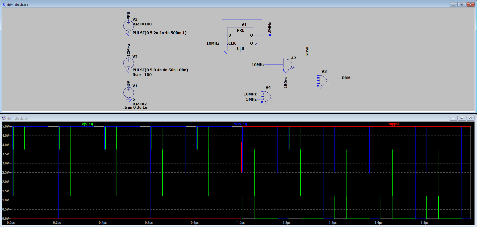
I think I should be able to use the PPS rising edge to set a flip flop, and reset that with the rising edge of the next 5 MHz pulse, but I think I would need an edge triggered SR latch for that which isn't something that exists as far as I can tell.
(As a sidenote, I'm noticing propagation delays are coming into play here, even with high speed logic gates (~5ns Td), but I don't think that's going to cause problems since all sites will be using the same hardware) -
Logic experts - still looking for help on this one (might move to a different subforum since we're all analog RF people here, hah)
I'm trying to figure out the best way to gate that 150ns pulse once, on the rising edge of the 1 PPS signal. I have basically no logic design experience so I'm really struggling to even search for the proper terms to get me started.
Here's my starting signals, separated this time so you can actually see what's going on: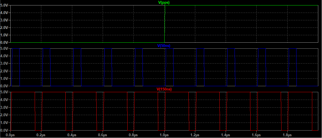
And here's my extremely accurate bespoke diagram of the signal I'm hoping to end up with: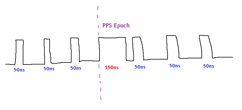
I think the idea mentioned earlier about a counter is a good start - clocked using the 10 MHz, started at the PPS epoch, and stopped after 3 cycles, but I'm at a total loss as to how to actually design that. -
How wide does the 1pps need to be? At the moment you've zoomed in and the 1pps appears as a step. Can the 1pps be a 150ns wide pulse?
-
How wide does the 1pps need to be? At the moment you've zoomed in and the 1pps appears as a step. Can the 1pps be a 150ns wide pulse?
It's currently a 500ms pulse but the uBlox NEO modules I'm using do have a programmable pulsewidth. However I don't think I'd trust their accuracy down to the ns level which is why I'd like to derive the pulsewidth from the 10 MHz clock and just "trigger" the wider pulse from the rising edge of the PPS signal regardless of its pulsewidth. -
If you really want a quick and dirty circuit, and only the rising edge is important, then you might be able to use a 50ns monostable and a 150ns monostable, and "or" the outputs to form the composite signal.
-
I'm thinking what I might do is use a monostable multivibrator as the "gate" signal to gate in the more precise 150ns pulse I'm already generating. I won't care about the precise pulse width of the gate signal as long as it's longer than 150ns and less than 250ns (so it doesn't extend the following pulse) which means I don't have to be super precise with my RC value selection.
Going to try and simulate this today to see what I can come up with. -
Did this get cleared up? It seemed like an interesting idea with maybe a simple solution. Been thinking about it for a while, no simple solution I could see. But I've modelled what looks like a complex solution in ltspice which IN THEORY could be implemented with 2 x 74HC74 dual flip-flops and 1 X 74HC00 quad nand gate. Which is not a big investment. I say in theory because I'm not sure if gate delays will introduce glitches.
I'm not sure how to pass it on. I will attach the ltspice diagram and the output waveform.
An explanation. V1 is a 1MHz pulse train (I don't know the characteristics of the generic ltspice digital models so I chose something slower than 10MHz). V2 is an emulated 1pps, but much faster so several extended pulses appear in a short time. V5 is a logic 1. Used by the generic AND (used here as a NAND) gate which has 5 inputs, only two are used so the rest need setting to logic 1.
When no 1pps is being processed, the pulse signal path is through nand A3 where it gets inverted, then through nand A4, which inverts it again. Only one pulse out of 2 is required, Flip-flop D1 manages this as its output is half the input, it enables A3 via A2 every second pulse.
When a 1pps is detected, the first part of the output pulse is just passing the input pulse. D1 Q goes high, all inputs of A2 are high including the input from V1, meaning A2 is acting as an inverter of the signal from V1 and outputs a low. D4 has not yet received the information about the 1pps so its Qbar is high, all inputs of A3 are high except the input from A2, so A3 outputs a high (the original pulse).
The 1pps detection is done by D2 - it is set by the rising edge of V3. To synchronise this with the pulse train, its value is passed to D3 on a rising pulse from D1. D3 latches D2, D2 output is no longer required so D3 resets D2. A1 is used as an inverter so that D4 latches D3 on a falling edge of the original input pulse. Having latched the D3 value, it resets D3. The D4 Qbar value, which most of the time is high, goes low. It causes A3 to putput a high regardless of the value from A2, until the next falling edge of the input. This extends the output by one cycle of the input.
-
I had further thoughts about this. When the delay caused by real world gates is taken into consideration, the "solution" I gave yesterday may be unworkable.
Problem 1. There is a delay in D1, A2 will not pass on the input pulse until D1 Q goes high, but the tail end of the input is not delayed so the pulse is shortened.
Problem 2. Delays propagating from D3 to D4 might cause D4 Qbar to be delayed too long causing a glitch between the original pulse and the extended pulse.
Problem 3. For the same reason as Problem 2, the extended pulse is too long.
All this can be addressed by rejigging the circuit, but I can't model all of it in ltspice.
Solution to problem 1. Clock D1 from the inverted pulse from A1. This means the rising input pulse happens well after D1 Q goes high, and D1 will lower Q after the falling input pulse. So the full pulse passes through A2, A3. If the delay in rise and fall times is equal, the output pulse is the same length as the input pulse, just delayed by two gate delays.
Solution to problem 2 and 3. D3 can be clocked by the output of A3 and cleared by an RC circuit from D3 Q slightly less than 150ns later. D flip flops can be used this way as one shot, especially ones with schmitt-trigger inputs. The output of D3 Qbar goes to A3 instead of the output of D4. D4 is not required. The D3 Qbar transition occurs within the high of the input pulse so A3 will not glitch. The RC constant is calculated to give the right pulse extension.
D3 could be replaced by any one shot that has an enable (the output of D2). Depending on its output, there is a spare gate on the quad nand that could be used as an inverter.
Is it worth continuing this thought thread?
I've attached the ltspice diagram with Problem 1 solution. The pulse extension still works in ltspice but unlikely to in reality.
-
I was able to find a 74HC library for LTspice that has realistic behaviour for the devices. The simulation gives the desired result. The simulated input was changed to 10MHz so the modelling includes realistic delays. A timing pulse arrives at an arbitrary time (to prove it always produces the right output pulse). The output looks like 5Mhz 50ns pulses, with the timing pulse extending the 50ns to 150ns (about).
The "about" is because the extension is dictated by the RC values (2kohm, 68pF) and the characteristic of the reset on a 74HC74. In the simulation, the reset pin drops to 2.5V before a reset is triggered. It is likely a real 74HC74 has a different trigger and the RC would need adjusting accordingly. The point is, it works.
The final circuit is attached for your perusal and any comments.
-
Sorry for not seeing your replies sooner! This is still an "on the backburner" project, one of many I've got. You know how it goes sometimes haha.
I will definitely take a look at what you proposed. I appreciate the effort! I would definitely consider a couple of logic chips to be a relatively "simple" solution. -
I suggest getting a 10 MHz GPSDO and using a pair of MCU timers to generate the output pulses. You can do it all with just the GPSDO, 50 MHz BP filter and some output buffer amplifiers.
This is happily, one of the easiest MCU programs possible. One step above blink a single LED. Blink 2. There are a slew of cheap MCUs that clock at 50 MHz and faster.
If the GPSDO has a fast rise time (most do) you could filter the GPSDO square wave to pick off the 5th harmonic, resquare it and clock the MCU with that. It *should* be edge synchronized with the GPSDO. Though there is a strong "actual mileage may vary" component to every MCU I've played with.
Have Fun!
Reg -
I suggest getting a 10 MHz GPSDO and using a pair of MCU timers to generate the output pulses. You can do it all with just the GPSDO, 50 MHz BP filter and some output buffer amplifiers.
I did consider something like this, but thought 3 logic IC would be simpler.
This is happily, one of the easiest MCU programs possible. One step above blink a single LED. Blink 2. There are a slew of cheap MCUs that clock at 50 MHz and faster.
If the GPSDO has a fast rise time (most do) you could filter the GPSDO square wave to pick off the 5th harmonic, resquare it and clock the MCU with that. It *should* be edge synchronized with the GPSDO. Though there is a strong "actual mileage may vary" component to every MCU I've played with.
Have Fun!
Reg
Various PIC processors have an internal PLL to multiply the oscillator by 3 or 4. There may be processors that do other multiples. Saves all that filtering. I couple into the GPSDO OCXO output after being buffered in a 74HC04. Just needs a 22pF cap to the clock in.