-
That would be the HP 54600 series scopes.
Its a digital scope so it was easy to add it in as a easter egg in the firmware. -
Yeah, I thought about that! I've never home etched a complex double sided board before, what do you think is the smallest hole most people can reliably drill at home with a cheap drill press?
I know this will sound big and ugly, but make the hole at least 12mil, the outer diameter 30mil. The reason for the huge size is that when exposing home made boards, the top and bottom layer aren't always perfectly aligned and also when drilling though, a slight error in alignment can push off the copper pad on the other side if it is too thin.
The smallest I would go would be 10mil drill with 26 mil outer diameter, but, the above measurements would be better.
Careful with your transistor & passive component library, make sure they don't have smaller holes than what I've listed above.
For transistors, make sure the TO-92 has a the wide off-center center pin footprint spacing. Since we might need to solder on the top and bottom, if the center pin is pushed back, soldering on the top of the PCB is much easier to do without shorting to the 2 adjacent pins. Everything else should be easy to solder on both sides.
For the traces, I would mostly route 12mil, saving 10 mil when going under 1206 smd caps and resistors & sot23.
Thanks! Seems like good advice. When you talk about a wide off center trace for TO-92, do you mean like would be used for "Ammo Pack" style pre-formed leads? Or do you mean more TO-18 style where the center pin is vertically off center from the other pads?
So, I've decided to go mostly through hole, with some SMD. The JFETs will be SOT-23 due to availability and cost; tantalum caps will be SMD size D mainly due to cost (for example, a 100uF TH tantalum costs between $3 and $5 from Digi-Key, whereas a surface mount version would be less than $1). -
Thanks! Once I get back to my computer tonight I'll grab those. That'll make it a lot easier to convert. I can also send you the DipTrace schematics in PDF form if you don't want to download DipTrace. (I've got Ghostscript setup as a PDF printer.)
My intent was just to share it with the forum community. I figure once the boards are done, I'd see how many other people want them, order a batch and then order enough parts to do them all. The parts will obviously be a lot cheaper if ordered in larger quantities. (If just five people are interested in kits the price can be almost cut in half!)
I'm doing this because I think it's an awesome project and I want one myself! It's also a bit of a challenge to do layout for. I'm not looking to commercialize it or to make any money off it; any parts kits would be sold to forum members at cost.
I did plan on releasing the Gerbers and a full BOM though, assuming you're alright with that.
That's all cool. I don't care if you actually make a few trivial bucks here; it's just about fair use of IP, not any anti-capitalist ideology.
The last time I did something like this I sold off the boards above cost (though not by much); not as a money making endeavour as it hardly compensated my time invested (post office trips, filling out customs forms, blah, blah) but just to ensure that after sundry expenses (variations in postage costs to different countries, fuel for 6.3L car engine, etc) the endeavour wouldn't see me in the red.
Heck, if it means enabling half a dozen other members here to get duplicate builds up and running I think you could fairly recoup the cost of your own build; it would only be a knob that would get enviously or narky at you for that.
Oh yeah, totally. I'd planned on putting your name and a link to your site on the boards anyway, crediting you with the circuit design. You clearly put a ton of thought and effort into the design, so you deserve the credit.
So, a couple of questions I've come up with as I've been capturing the schematic:
Is there any particular reason the main rails are +-14.3V instead of, say, +-15V? I'm sure there must be some reason, so just curious.
Should a 20V rating be alright for the polarized caps? I can't see any place that the full 28.6V (between V+ and V-) would go across them. -
+/-14.3V is just what the power supply delivers; will still operate fine on +/-15V rails. A 20V rating is adequate for the polarised caps.
-
WoW very nice!!!
At university we had an HP scope (I don't remember model) with tetris, scope games are awesome
Machine vs machine ends at some point or goes to max freq and still playing?
Hits full speed and just keeps going. -
+/-14.3V is just what the power supply delivers; will still operate fine on +/-15V rails. A 20V rating is adequate for the polarised caps.
Thanks! I just wanted to make sure I wasn't missing something.
-
Thanks! Seems like good advice. When you talk about a wide off center trace for TO-92, do you mean like would be used for "Ammo Pack" style pre-formed leads? Or do you mean more TO-18 style where the center pin is vertically off center from the other pads?
I believe it's the TO-18 style, like this:
O
O O
This makes it easy for a hand soldering of a home made PCB where you can now soldier all 3 legs on the bottom and top without having your weller tip squeezing between 2 pins to solder the center pin.
-
(for example, a 100uF TH tantalum costs between $3 and $5 from Digi-Key, whereas a surface mount version would be less than $1).
Aren't through-hole electrolytics the cheapest?
Question for GK, Should we be using electrolytics or tantalum caps in your circuit?
I know they slightly behave differently with ESR, voltage VS cap value and temperature.
-
Agree with BriangHG, anyway they will be manually soldered one by one.
TO-18 triangle placed pins are easier to solder even with big soldering iron than single line of 3 pins TO-92s.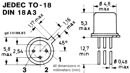

Besides, abit of bending the middle TO-92 pin to fit it isn't that big deal, unless its automated. -
Remember, you used to be able to purchase TO-92 with the center lead bent back already.
Ok, because of tape and reel, today, you have only these flavors A and B, C is rare: (All are top view)
A: (Too difficult to soldier on a home-made PCB)
000
B: (Easier to solder on a home-made PCB)
O O O
C: (Obsolete, but easiest to solder + you can get a fat 10 mil trace between the pads with good clearance):
2
O
O O
1 3
We would just end up purchasing type B and bend the center leg back, or type A and push it in like a tripod...
Careful, TO-18 might have pins 1&3 reversed, double check before blindly using that transistor footprint. Just use type B's footprint, modify the center pin by pushing it up by 2.54mm.
-
(for example, a 100uF TH tantalum costs between $3 and $5 from Digi-Key, whereas a surface mount version would be less than $1).
Aren't through-hole electrolytics the cheapest?
Question for GK, Should we be using electrolytics or tantalum caps in your circuit?
I know they slightly behave differently with ESR, voltage VS cap value and temperature.
I think there are two or three tantalums recommended on the schematic, the rest are electrolytic.
I need to go back and count, but if it's only one then I guess TH wouldn't be a problem cost wise. (Sorry, laying out PCBs for a living has made me very sensitive to parts costs, I know it's not as big of a deal here, it's a hard habit to break!)
Edit: Counted, my bad, it's just one! -
Remember, you used to be able to purchase TO-92 with the center lead bent back already.
Ok, because of tape and reel, today, you have only these flavors A and B, C is rare: (All are top view)
A: (Too difficult to soldier on a home-made PCB)
000
B: (Easier to solder on a home-made PCB)
O O O
C: (Obsolete, but easiest to solder + you can get a fat 10 mil trace between the pads with good clearance):
2
O
O O
1 3
We would just end up purchasing type B and bend the center leg back, or type A and push it in like a tripod...
Careful, TO-18 might have pins 1&3 reversed, double check before blindly using that transistor footprint. Just use type B's footprint, modify the center pin by pushing it up by 2.54mm.
OK, that sounds like a good plan. I agree type C is easier to solder, as they tend to stay in the PCB due to pressure from the leads pre-solder.
Type A is TO-92 JEDEC standard straight lead bulk; type B is called TO-92 2.54mm spacing lead form, "ammo pack" tape and real.
Type A are generally sold loose whereas type B comes taped on those thin cardboard bandoliers (hence ammo pack) that we all hate because it leaves a sticky residue on the pins!
Edit: By the way, I appreciate any and all advice on this. It's been quite awhile since I've laid out a mostly TH board designed for hand soldering. I realize doing kits designed for hand soldering and potential home etching is a lot different than boards designed for production, so these sort of tips are good reminders.
-
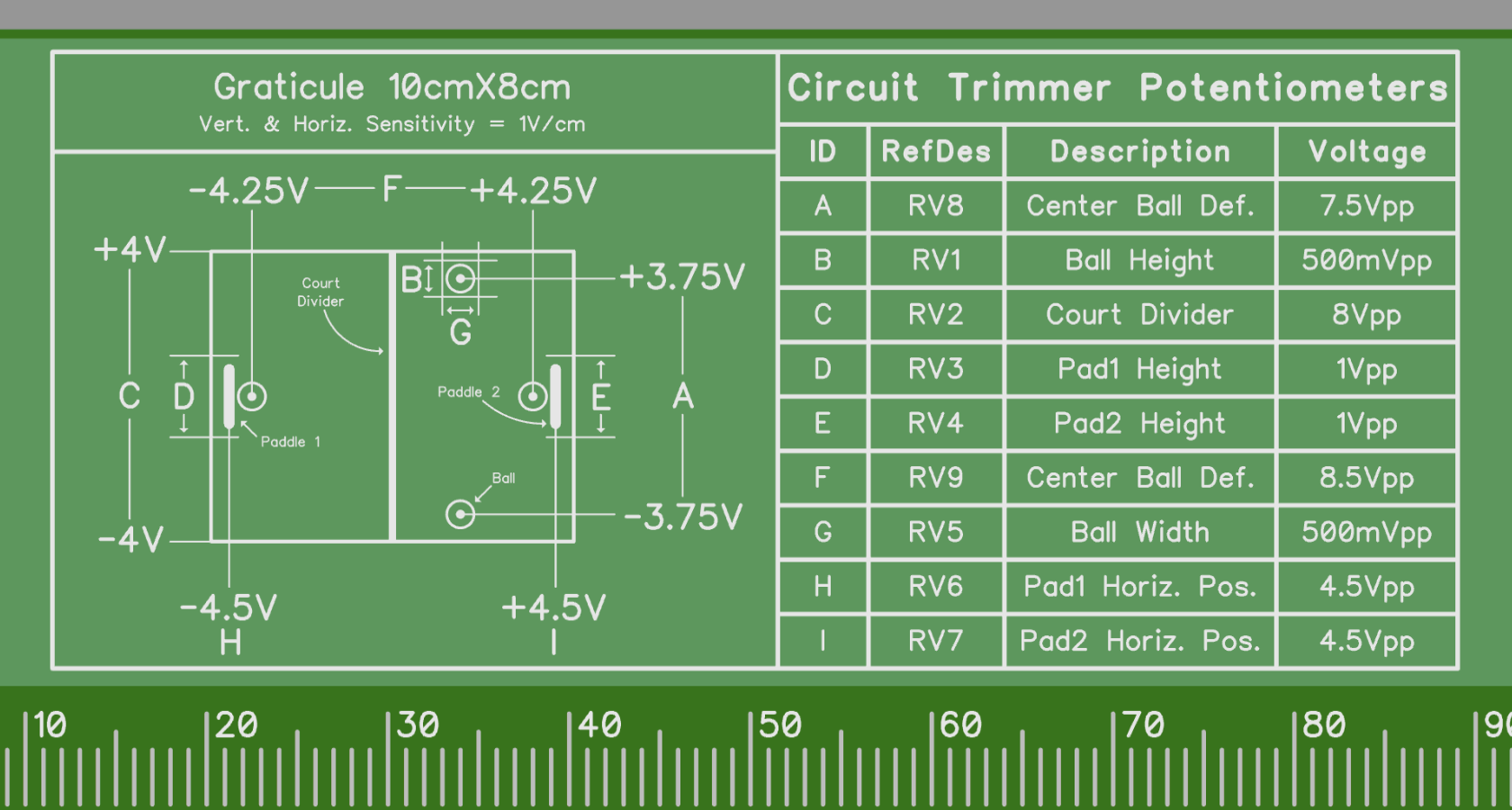
So, I had some time this afternoon while waiting for an appointment to redraw GK's trimmer diagram on my iPad in a vector drawing app. This is for inclusion on the schematic and possibly the silkscreen of the power supply board (since I'll have some free space there; it could also be done on the copper layer instead of silk, if those etching at home want it on their boards).
-
So, I had some time this afternoon while waiting for an appointment to redraw GK's trimmer diagram on my iPad in a vector drawing app. This is for inclusion on the schematic and possibly the silkscreen of the power supply board (since I'll have some free space there; it could also be done on the copper layer instead of silk, if those etching at home want it on their boards).
That looks good, but it might cause come confusion as the ball positions at the ends of "A" are not to scale as the circumference of the ball does not touch the boundary.
-
The only specified tantalum is the 100uF timing cap in the velocity integrator schematic. I specified tantalum here for the (generally) lower leakage as the capacitor is linearly charged with a rather small current (several uA). All of the other polarised capacitors can be electrolytic.
The 1uF integrator capacitors in the horizontal and vertical movement circuits shouldn't be some crappy Z5U/Y5V/etc dielectric and you probably wouldn't want to pay for COG/NPO here. The best pick is a TH polyester. 1uF is readily available in 5.08mm lead pitch in the required voltage rating range.
Similarly of the capacitors marked "*" "Polyester" in the function generator schematic can alternatively be COG/NPO ceramic types if going SMD as the capacitance values are small and the price relatively cheap - definitely do not substitute these with Z5U/Y5V or the like. -
Incredible project. I want to be like you when I grow up... my wife is not sure when that will be, though.
-
So, I had some time this afternoon while waiting for an appointment to redraw GK's trimmer diagram on my iPad in a vector drawing app. This is for inclusion on the schematic and possibly the silkscreen of the power supply board (since I'll have some free space there; it could also be done on the copper layer instead of silk, if those etching at home want it on their boards).
That looks good, but it might cause come confusion as the ball positions at the ends of "A" are not to scale as the circumference of the ball does not touch the boundary.
Ah, good catch. I'll fix that.The only specified tantalum is the 100uF timing cap in the velocity integrator schematic. I specified tantalum here for the (generally) lower leakage as the capacitor is linearly charged with a rather small current (several uA). All of the other polarised capacitors can be electrolytic.
The 1uF integrator capacitors in the horizontal and vertical movement circuits shouldn't be some crappy Z5U/Y5V/etc dielectric and you probably wouldn't want to pay for COG/NPO here. The best pick is a TH polyester. 1uF is readily available in 5.08mm lead pitch in the required voltage rating range.
Similarly of the capacitors marked "*" "Polyester" in the function generator schematic can alternatively be COG/NPO ceramic types if going SMD as the capacitance values are small and the price relatively cheap - definitely do not substitute these with Z5U/Y5V or the like.
Just to clarify do you mean standard polyester film/foil or polyester metalized?
I assume metalized is OK (I've used metalized PET caps in S&H circuits before, so I assume that'll be fine.) -
PET, being the most economical and physically compact (generally), is the logical choice.
-
PET, being the most economical and physically compact (generally), is the logical choice.
Okay, good, that's what I had specified. -
Are you taking orders yet?
I'm in like Flynn. -
Okay, so I've got about half the schematic done now (haven't started on layout yet) and I've settled on pretty much all through hole (the JFETs being the only exception). I've calculated the area the design should take and I'm confident I can fit it on two 200x200mm boards (which will cost under $10/ea).
If there's any issues with home etching a board that size, I could always split the design up into four 100x100mm boards, but that would add some complications when it comes to interconnecting them.
Here's a 3D view showing the size of components for three of the smaller sections of the circuit. Obviously the actual area used will be larger due to routing constraints, component placement, etc.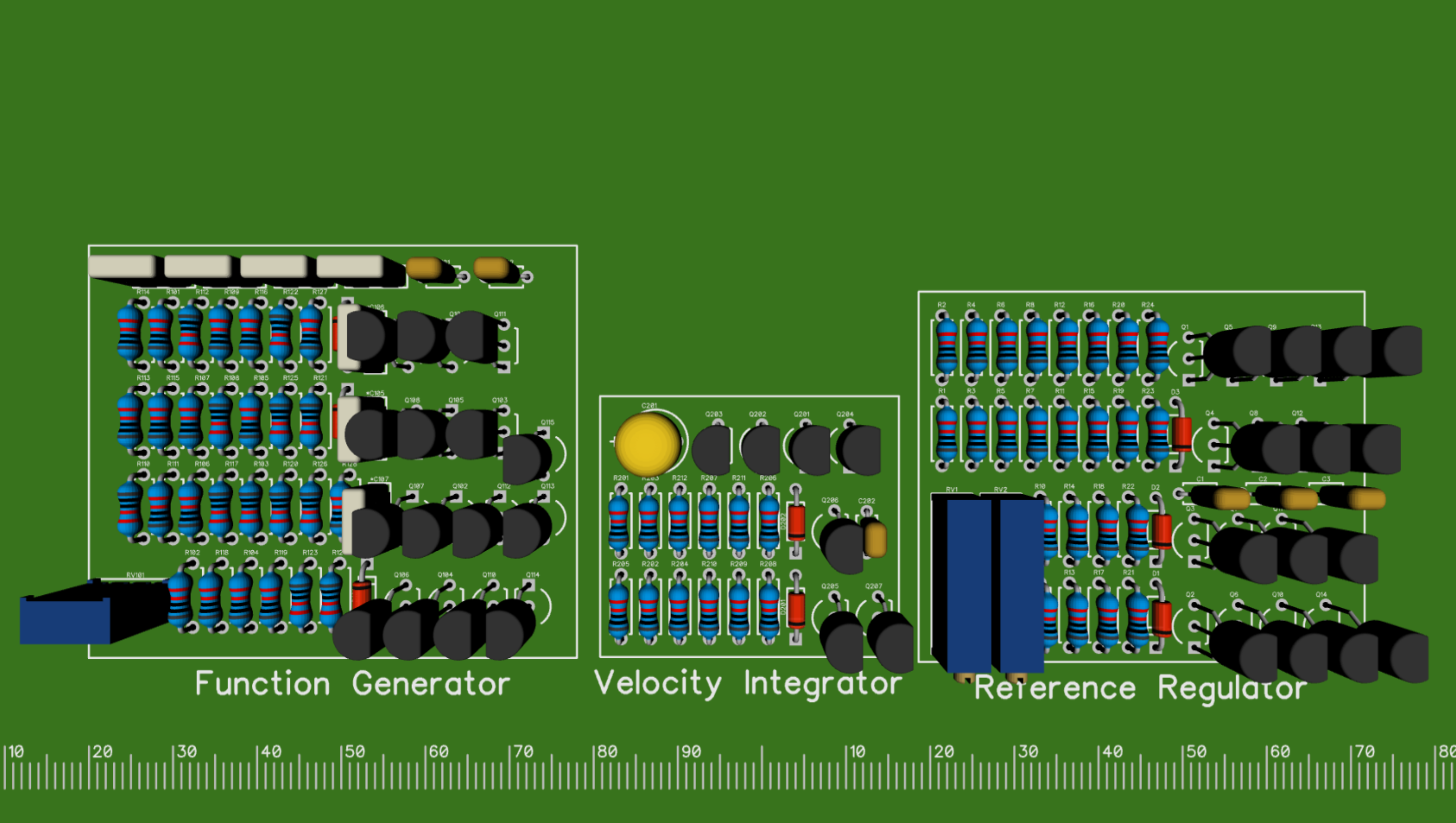
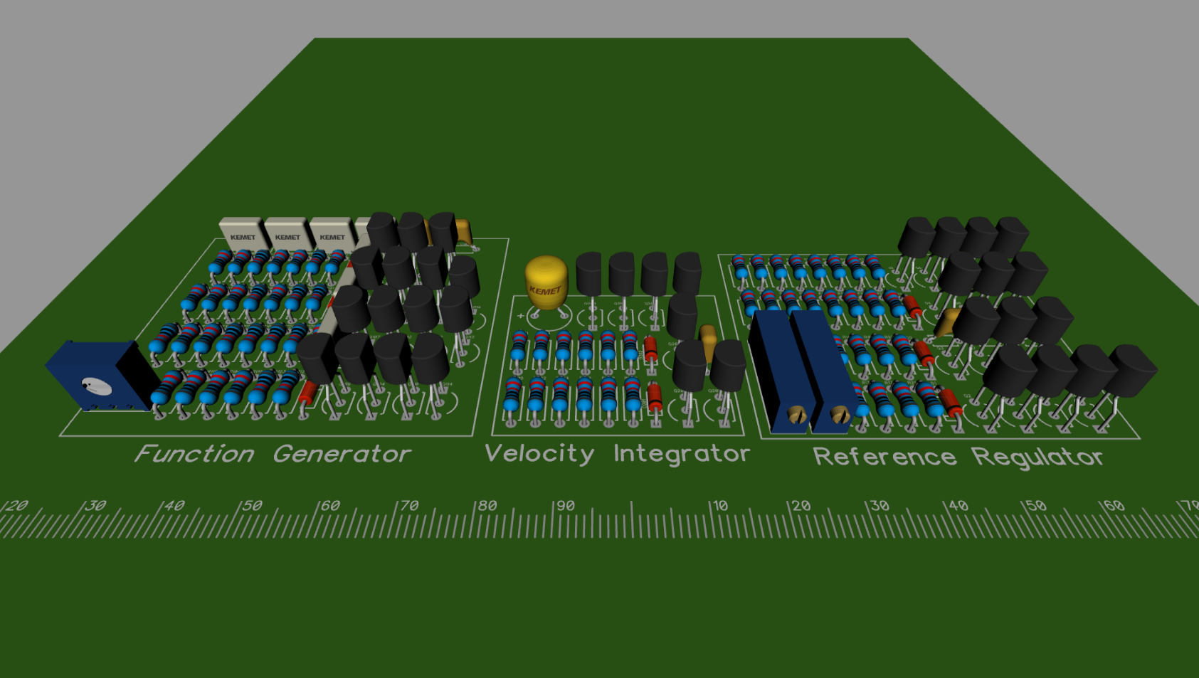
I still need to go in and change the footprint for the TO-92 transistors, but the footprints and pad spacing for everything else is correct. I'm planning on using a 7.62mm spacing for the resistors. I know that normally you wouldn't want to bend the leads right at the part like that (rather you'd use a 10.16 spacing) but this isn't going to be mass produced or subject to a high vibration environment or anything, so the space savings really adds up. If there's any objection to this I could always use a 2.54 vertical footprint, but I really dislike that as it's a pain in the ass when soldering, as they don't stay in the board when soldering and are subject to more bending stress. -
For your trimmers, use vertical adjustable ones. This way, they don't need to be at the edge of the PCB, they can be easilly adjusted where ever you wish to position them. The vertical 10/25 turn trimmers also take less PCB space. Also, since you can't solder between the trimmer and top of the PCB, when wiring those, try to prioritize routing them on the bottom of the PCB.
-
I also think vertical trimmers are better for this
Also i think the layout of the components should be made so that it roughly resembles the schematic rather than going for the old school tidy all resistor in a row thing. Even if it means using resistors mounted standing up (I think such resistor mounting has a certain oldschool charm to it).
Oh and don't forget test points. I would put lots of those solder in eyelet test points all over the circuit to allow for easy testing of the blocks as well as use test points on most interblock connections so that one can see how the circuit works.
-
I think timb's current rendered layout is just for space approximation at this point. To generate a nice 2 layer PCB without spaghetti traces, potentially creating some oscillators due to trace length looping around in odd ways, he will be forced to optimally re-arrange the components in each function block when routing.
-
Oh and don't forget test points. I would put lots of those solder in eyelet test points all over the circuit to allow for easy testing of the blocks as well as use test points on most interblock connections so that one can see how the circuit works.
Yes, test hooks are planned.For your trimmers, use vertical adjustable ones. This way, they don't need to be at the edge of the PCB, they can be easilly adjusted where ever you wish to position them. The vertical 10/25 turn trimmers also take less PCB space. Also, since you can't solder between the trimmer and top of the PCB, when wiring those, try to prioritize routing them on the bottom of the PCB.
All the main trimmers that adjust the geometry (stuff in the adjustment diagram) will be vertical ones, as they will be on the top board. There are a couple of other trimmers that control other stuff (like the reference voltage, etc.) and they will most likely be on the bottom board, so I've got two options there:
1) Use vertical trimmers and place a hole in the top board for an adjustment tool to fit through.
2) Use horizontal trimmers and locate them near the edge.
I don't think it's more than a couple of trimmers that will need to be on the bottom, so I may go with option 1 if I have enough space to include the holes. (I'll decide during layout.)
The reference trimmers will most likely be towards the edge of the board anyway, that's why I ended up specifying 15 turn horizontal cermet trimmers for that, but I can always change it during layout.I think timb's current rendered layout is just for space approximation at this point. To generate a nice 2 layer PCB without spaghetti traces, potentially creating some oscillators due to trace length looping around in odd ways, he will be forced to optimally re-arrange the components in each function block when routing.
This. That's just how the components happened to group together when importing from the schematic. As you say, I will be forced to arrange things for optimal layout. This is due to a number of factors, including: Keeping trace lengths as short as possible, routing constraints on a two layer board, component pinouts, etc.