It isn't all analog, either. Sure, the graphics are drawn though a combination of sine, cosine, triangle and square waves generated by discrete integrators and op-amps, but that's not the end of the story... It's also full of discrete digital components as well; flip-flops, logic gates, inverters and latches! There are also comparators, which are half-digital (kind of). In fact, I'd say at least half of the circuits are digital in nature.
True of course. What I meant was that the whole circuit is built only from discrete analog components - some are indeed built into sub-circuits that form the basic digital building blocks you mention - but there are no logic gate ICs in there, and for me that really adds to the charm of the project.
Now, if you go and add a 7-seg driver built out of discrete transistors that could be interesting...

Now, if you go and add a 7-seg driver built out of discrete transistors that could be interesting...
Not that hard - 1 of 10 counter and a diode matrix to decode.
Maybe use multiplexing to share the diode array between digits. Single digit per player would keep things more sensible.
Diodes are cheap, just use one set per digit, you only need 44 per digit to fully decode 0-9, and 10 driver transistors to provide segment current.
Now, use that to drive a sexedecimal display and multiplexing would be worthwhile to share the decode logic between them.
Challenge is to have a on screen display with player names.
Challenge is to have a on screen display with player names.
.. with international character set, including Chinese,Thai,Arabic,Hebrew etc...
Core rope memory perhaps.....
Okay, so I didn't get nearly as much done as I planned tonight, feeling a bit under the weather so I decided to make an early night of it.
I finished the Function Generator section, but forgot to upload the PDF/images for them, doh!
I also did the Multiplexer FET Gate Drive section; I implemented it as a sub-section of the Multiplexer Logic; the Horizontal and Vertical section will be placed directly above the Multiplexer section. That way the X, Y and Z BNC connectors will all be facing the same side on one board.
I also added some test points and cleaned up some traces in the Multiplexer Logic section.
Hi Tim. You're making some good progress, but there are some important layout points I should probably interject here with. In the gate drive circuit there is associated with each JFET pair a 20k resistor terminating the gate terminals to ground and a commutation diode. In your schematic these are R1101, R1105, R1109, R1113, D1101, D1102, D1103 and D1104.
When a JFET pair is turned ON its respective commutation diode is reverse biased and the gates are effectively isolated and terminated to ground through the respective 20k resistor. We don't want this termination resistor to be half a board width away with a long inductive track in between. And although the discrete op-amps in the horizontal and vertical deflection circuit do not have a super high GBWP, it is still good practice to minimize the virtual earth nets.
These requirement make it necessary to bunch up to some degree the JFETs and their associated gate diodes and resistors around the inverting inputs of the respective op-amps. Attached is a scribble of a quick/rough diagram approximating an acceptable layout that meets these requirements.

The length of the logic-level digital control lines emanating from the cathodes of the gate commutation diodes really doesn't matter; it's just these components that you have to keep reasonably compact.
Okay, good to know. My plan was to start building out the H and V circuit literally right from where the Gate Drive circuit currently is, so the GATE0-3 nets won't be routed more than an inch or so. Basically I'm making the Multiplexing Logic, FET Gate Drive and H&V Deflection circuits one single super-section as far as the layout is concerned, if that makes any sense? I figure that would best preserve signal integrity and make the layout most compact.
Edit: Though I will most likely move those gate diodes and resistors so that they're as close as I can get them to the associated JFET pair. Ultimately there will need to be at least a couple of inches of trace coming from the anode of the gate diode, since they split between the Horizontal and Vertical JFETs, which I can't easily mix since their outputs have to stay together to keep the the two virtual GNDs short. That said, they won't be running hundreds of mm across the board or anything.
Well, LEDs are still discrete. You could even make a 7-segment display with discrete LEDs if you really wanted (though I think some of those little HP bubble 7-segment displays wouldn't look out of place, and they *are* period appropriate).
IIRC, GK's original suggestion was to use discrete LEDs to make the 7-segment display (i.e., it's a 7-segment display in name, but each segment is comprised of discrete LEDs).
Edit: Though I will most likely move those gate diodes and resistors so that they're as close as I can get them to the associated JFET pair. Ultimately there will need to be at least a couple of inches of trace coming from the anode of the gate diode, since they split between the Horizontal and Vertical JFETs, which I can't easily mix since their outputs have to stay together to keep the the two virtual GNDs short. That said, they won't be running hundreds of mm across the board or anything.
That sounds fine.
Something like this?
(Note: The board in those pictures is sized just big enough for that circuit, it's not the size of the final board and will be bigger.)
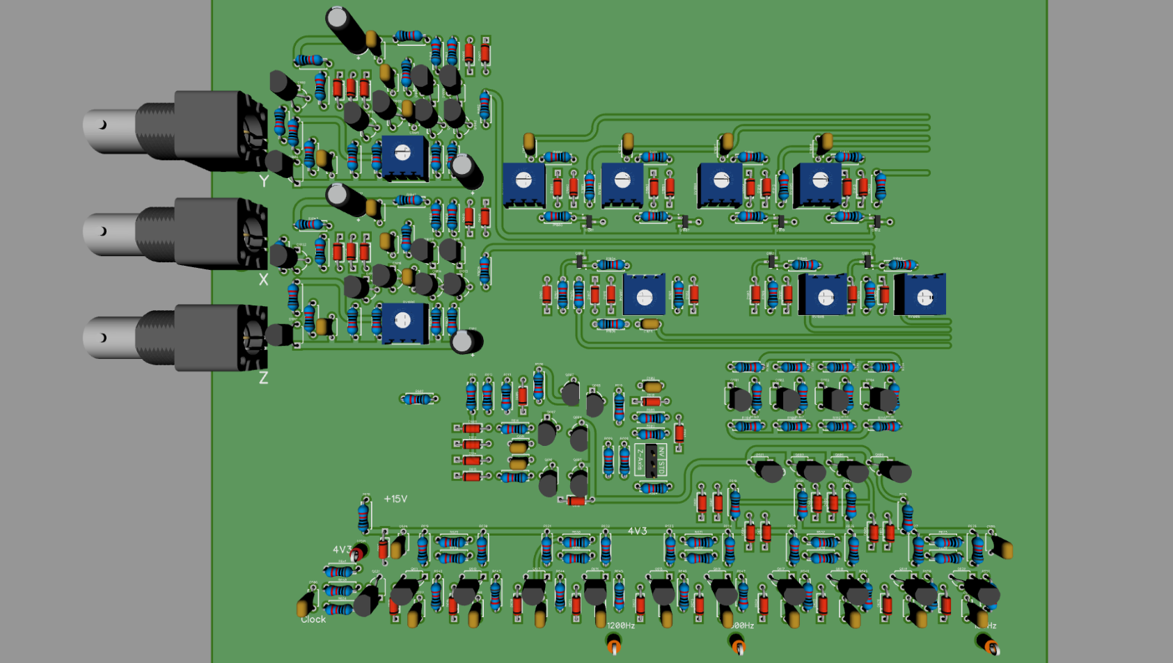
http://timb.us/PDF/Scope_Pong_XYZ.pdfThere's a couple of things in still not totally happy with and will go back to fix, but it's where I'm at tonight. So, the gate diode and resistor is right next to one of the JFETs and no more than 20mm from the other. Hopefully that will suffice?
I'm not happy with how long common lines that feed from all the JFETs to each deflection amplifier are, but it's the best I can do for right now. I may have a way to shave about 20mm off each, so I'll try that out later today.
OK, I can see what you've done there in an attempt to minimise the track length between the gate leads of each JFET pair, but really an inch or two of track length here won't hurt. What I was trying to emphasize in my prior post is that the JFET digital control lines on the anode side of the commutation diodes actually become sensitive analogue lines, so it's just important not to route them over long distances amongst other circuitry such as the digital stuff.
I don't think that your layout would cause any problems, but I'd personally rotate the JFETs 90 degrees and position them in a row as shown in my scribbled diagram, with the gate control lines running parallel to the in-line JFETs. I think this would permit a more optimal minimisation of the virtual earth nets whilst still keeping the gate nets adequately short and well confined to the analogue zone. Incidentally the way I laid out my rats nest version was as per that scribbled layout.
Yeah, rotating the JFETs is preciously what I was thinking of doing. I'll give that a shot tonight.
It's still a bit of a work in progress, but I thought I'd share where I'm at:
 http://timb.us/PDF/Scope_Pong_XYZ_V2.pdf
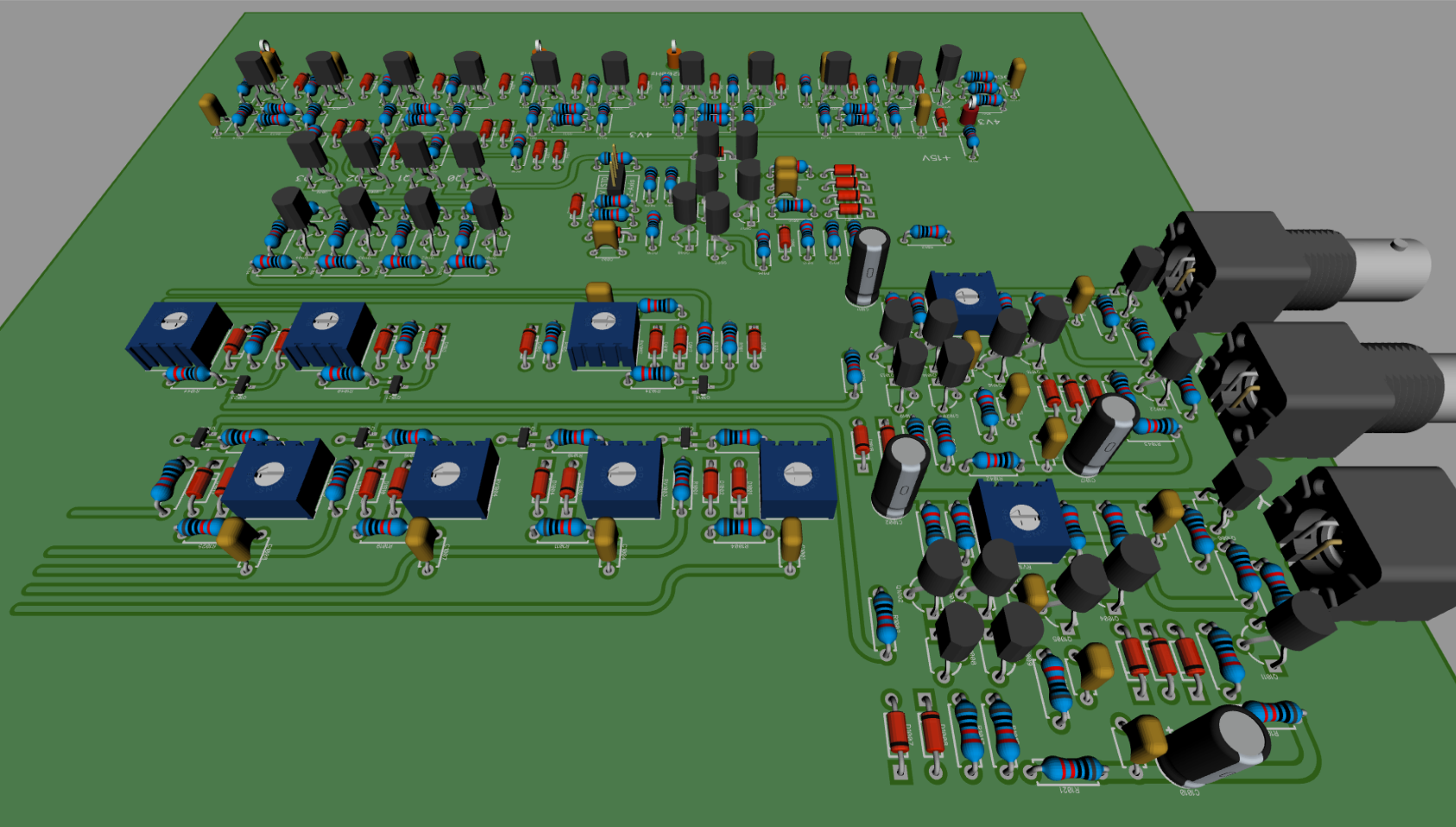
So the virtual GND net is a lot shorter, but the lines from the adjustment pot lines are a lot longer than before, which I'm currently working on shortening a bit. This new layout does give me about 1/4 more useable space than the previous version, so that's a plus.
I couldn't follow your recommended layout exactly, because the pinout of the SMD JFET is different than the TH version, so I had to make a few small orientation changes, but I think it's still better than before.
Nice...
Increase the outer diameter of the pads for the Z-Axis Inv select 3 pin sip, the rings are too thin.
Everything else is excellent.
Nice...
Increase the outer diameter of the pads for the Z-Axis Inv select 3 pin sip, the rings are too thin.
Everything else is excellent.
Oops, yeah, thanks for reminding me! I've been meaning to go back and fix that. (That's just a DipTrace built-in 1x3 Header pattern I used when making the Z-Select change to the schematic, I intended to go back and make a custom pattern with bigger rings.) Added to my to-do list!
I couldn't follow your recommended layout exactly, because the pinout of the SMD JFET is different than the TH version, so I had to make a few small orientation changes, but I think it's still better than before.
Keep in mind though that the virtual earth nodes extend to the drain side nets of the JFETs.
You can do my suggested layout like this:

For the center of that matrix, keeping the j-fet on the red layer, swap the blue and red trace layers inbetween, you will save on removing 1/2 the vias.
Okay, let me give that a try. I initially had something similar to that, but ended up changing it for some reason that I can't recall. I obviously overlooked something. (Man, I'll be glad when I get over this cold, or sinuses or whatever it is. My head feels like it's been in a vice for the last two nights and I just can't focus.)
Once I get that fixed up, I might go back and start routing some of the power and signal nets to the board to board connectors and do the power supply layout, which is fairly simple. Hopefully in a day or two I'll be feeling better and can finish the rest of the blocks. I've just got Horizontal and Vertical Ball, Paddle and Sound circuits left.
After staring at the layout for 15 minutes I totally see how I could have made that work; I don't know how I missed it. I just need to rotate a few things and twist something around. I can't believe I forgot both sides of the JFET are in the virtual ground. I mean it's a JFET, duh!

Keep well and get some early nights Tim, that's more important than getting it finished, yeah I know you have lots of us watching your progress (1) but it can wait.
1. 1125 guests watching.

Ha ha. These things inevitably happen after X amount of free-time hours successively crammed into one task without a break.... I wasted an hour or more debugging an entirely nonexistent fault with those JFET-multiplexed deflection amplifiers after I first built them. I was at one stage utterly baffled, then convinced that my JFETs were dodgy counterfeits as they all seemed to exhibit a decaying Id current tail at switch-off that seemed to defy JFET semiconductor physics...... but some spare SOT-23 MMBF**** soldered in to substitute behaved just the same.... In the end it turned out that my 10:1 CRO probe just wasn't properly compensated!
BTW, has anyone else noticed the crazy number of views this thread has had today? First thing this morning the topic view counter had not yet clocked over 10,000. Now, about 12 hours later, it's close to tripping past 15600!
I don't think this amount of traffic can be still coming from the Hackaday blog, as the mention is several-days-old news now and has scrolled well off the main page.


Probe compensation sanity check.

Keep well and get some early nights Tim, that's more important than getting it finished, yeah I know you have lots of us watching your progress (1) but it can wait.
1. 1125 guests watching.
I'm hoping it's just allergies, as there was a nice layer of pollen on my windshield today. The weather has also been crazy, freezing one day and cold the next, which never helps.
Ha ha. These things inevitably happen after X amount of free-time hours successively crammed into one task without a break.... I wasted an hour or more debugging an entirely nonexistent fault with those JFET-multiplexed deflection amplifiers after I first built them. I was at one stage utterly baffled, then convinced that my JFETs were dodgy counterfeits as they all seemed to exhibit a decaying Id current tail at switch-off that seemed to defy JFET semiconductor physics...... but some spare SOT-23 MMBF**** soldered in to substitute behaved just the same.... In the end it turned out that my 10:1 CRO probe just wasn't properly compensated!
Ah, the old probe compensation trap... I think we've all run into that before! XD
I really should take more breaks than I do (and I try to), but sometimes I'll sit down at 8pm and start working, the next thing I know it's midnight! And the only reason I even stop then is because my dog starts bugging me to eat.
BTW, has anyone else noticed the crazy number of views this thread has had today? First thing this morning the topic view counter had not yet clocked over 10,000. Now, about 12 hours later, it's close to tripping past 15600! I don't think this amount of traffic can be still coming from the Hackaday blog, as the mention is several-days-old news now and has scrolled well off the main page.
It's on the front page of Hacker News right now.
I couldn't follow your recommended layout exactly, because the pinout of the SMD JFET is different than the TH version, so I had to make a few small orientation changes, but I think it's still better than before.
Keep in mind though that the virtual earth nodes extend to the drain side nets of the JFETs.
You can do my suggested layout like this:
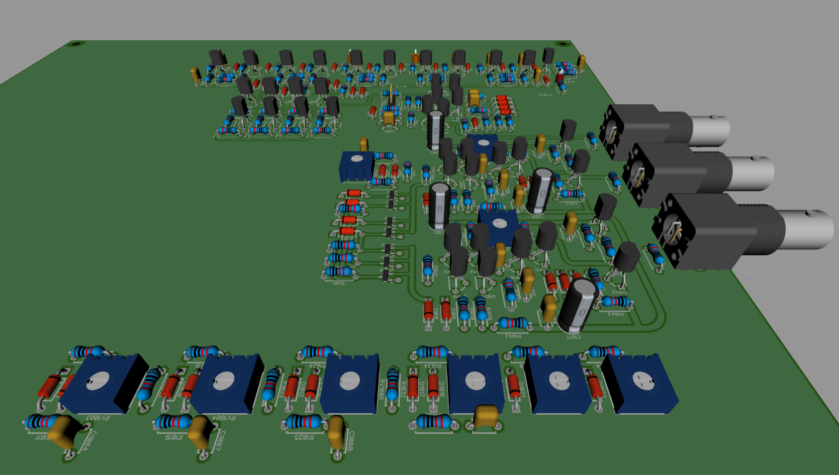
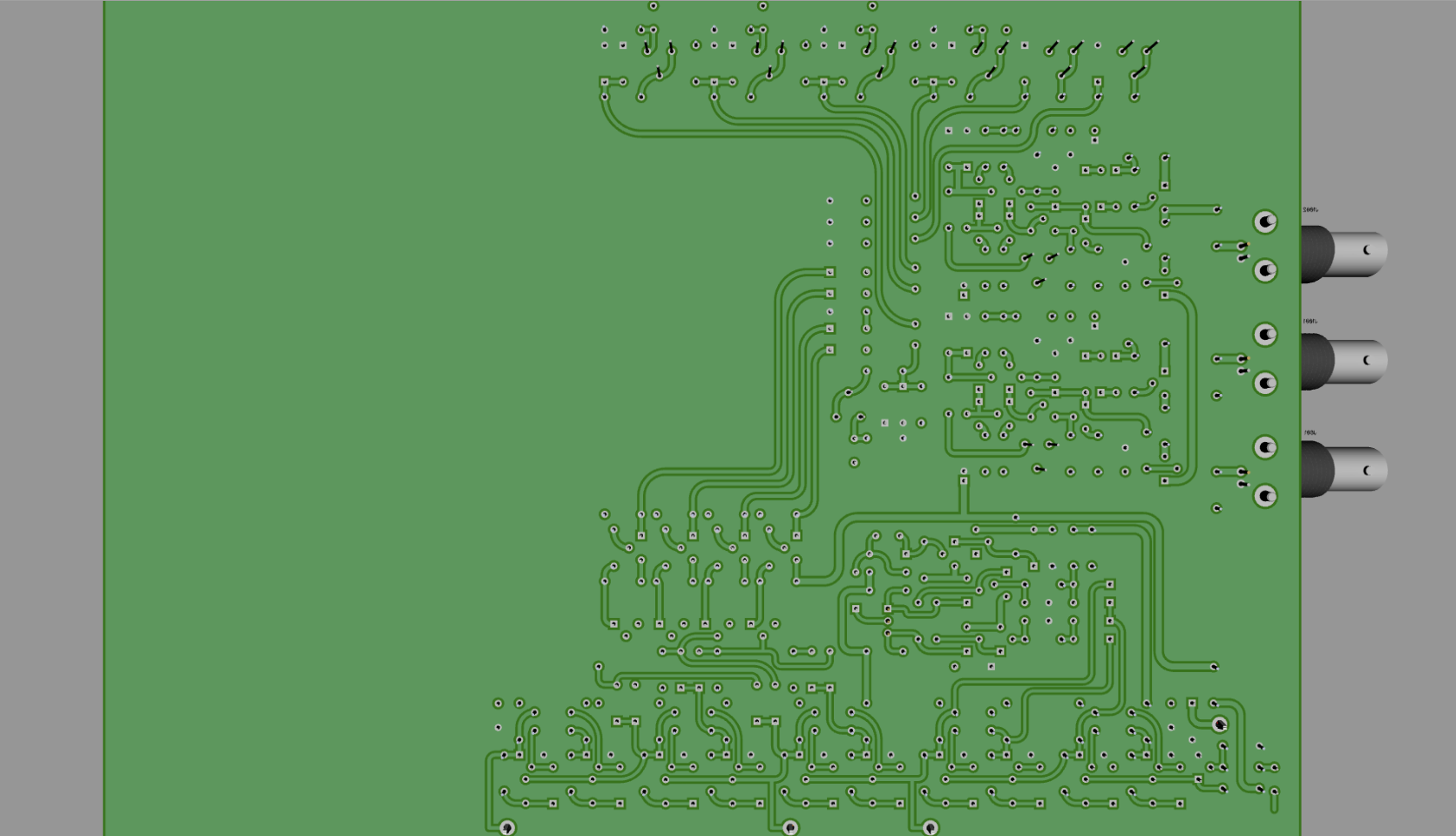
Okay, so here's what I came up with:
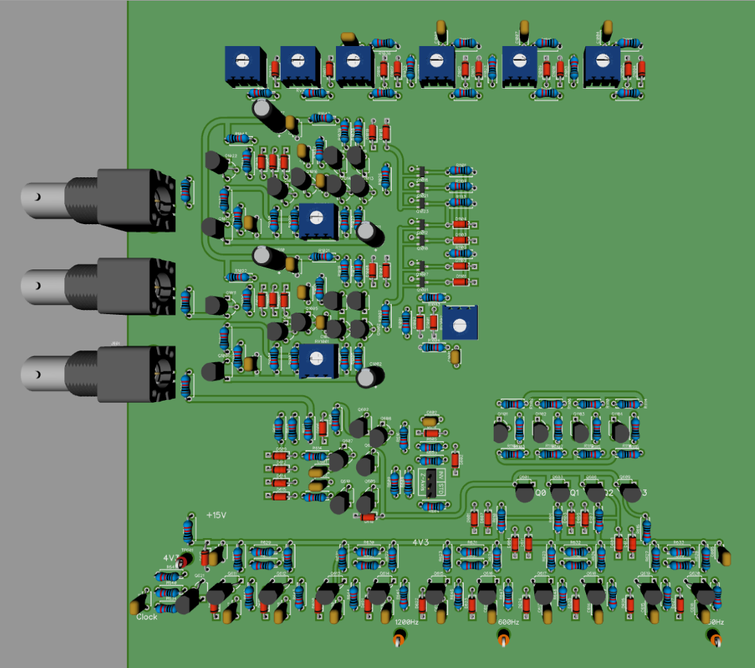
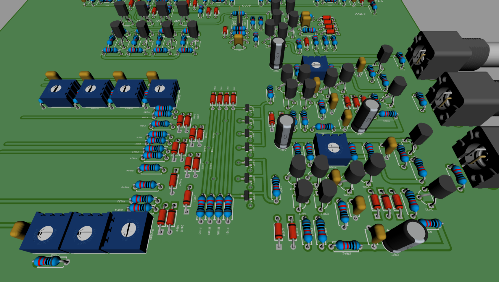 http://timb.us/PDF/Scope_Pong_XYZ_V3.pdf
I shifted the diodes around a bit to save space, but I still kept it very compact and the lines running to the drain nodes of the JFETs are each around 20mm. I still need to place the trimmers (ignore them in the image), but so far so good I think.