-
I've seen a surprising number of people not being able to do.
Are you talking in general or about kicad? If kicad I can imagine why. But I don't want to put it in dirt, at the end, this is the only opensource tool that is not totally useless. -
if you like to improve the GUI now is the time for it. The current 5.1.0 development is mainly about improving the overall user experience including finding and fixing inconsistencies. You will notice quite a bit of GUI changes compared to KiCad 5.0.0.
I could live with the GUI if I could just get better automated handoff of the netlist and live updating of the netlist (with an option to disable or perhaps undo the last import) among the various tools. The GUI is a collection of related apps that feels unpolished, but I have to admit that it's functional. (As is the netlist handling to be honest, so I'm even contradicting myself a bit there perhaps...)
I do not share your feeling how KiCad prioritizes work. Working on the GUI is only one of many things, and there are many things to do.
It's definitely functional and I can quite reliably get boards out of it. Any limitations with the tool are my own. -
Are you talking in general or about kicad? If kicad I can imagine why. But I don't want to put it in dirt, at the end, this is the only opensource tool that is not totally useless.
Mostly Eagle actually, and another older tool the name of which escapes me. I should clarify that I'm talking about hobbyists, not professional engineers. -
hah. you should see the schematics that are made with it ... if you think the Ui is bad ... ( i know , you can draw bad schematics in any package but the default libraries are .. total tripe. it shows that it comes from unix .. 50 years ago.)
Hop on circuitmaker. Free and it works. But.. beware of libraries. many symbols and footprint are wrong because they are cobbled together by newbies. i just did a design in Circuitmaker and had to redo EVERY SINGLE SYMBOL AND FOOTPRINT i used... Some parts are better than others but :
footprints:
- inconsistent layer assignments
- inconsistent line thicknesses
- 3d models on wrong layers, wrong 3d models, blobbed 3d models ( grey boxes) .
- missing courtyard , assembly layers , marker, fiducals
symbols :
- missing pins (especially thermal pads )
- mislabeled pins
- wrong pin numbers
- symbol pins not matching footprint pins.
- random pin lengths, upper case lowercase, special characters like mu and ohm sign that dont render properly
- using dots and commas in part values.
Once i loaded my library : smooth sailing. Got the boards made in china. works like a champ
-
if you like to improve the GUI now is the time for it. The current 5.1.0 development is mainly about improving the overall user experience including finding and fixing inconsistencies. You will notice quite a bit of GUI changes compared to KiCad 5.0.0.
I could live with the GUI if I could just get better automated handoff of the netlist and live updating of the netlist (with an option to disable or perhaps undo the last import) among the various tools.
I do not share your feeling how KiCad prioritizes work. Working on the GUI is only one of many things, and there are many things to do.
A feature was added awhile to automatically update the board from the schematic without going through the netlist-export/import steps. From either the schematic or the layout, choose "tools => update PCB from schematic." That will automagically generate the netlist from the schematic and import it into the layout using some defaults. If you use the separate steps of generating the netlist and importing it, you get more options.
Importing a netlist to update the layout is a pretty heavy-duty operation. My undo here is simply ensuring that any changes to the layout were committed back to my repository before the netlist import. If it's screwed up or I don't like it, I simply revert the changes.
I know the idea that when the schematic is updated (saved), the layout immediately updates to follow it. But there are many arguments against doing that (hashed out elsewhere) and I think that updating the layout only when you explicitly want to makes the most sense, at least for me.QuoteThe GUI is a collection of related apps that feels unpolished, but I have to admit that it's functional. (As is the netlist handling to be honest, so I'm even contradicting myself a bit there perhaps...)
It was a collection of programs that were put together in a suite, kinda like how many of the PCB layout tools started. Making the user interface the same across the tasks is ongoing development work.QuoteIt's definitely functional and I can quite reliably get boards out of it. Any limitations with the tool are my own.
same here. -
It's not about the quirks.
It's about the inconsistencies and KiCad is full of them.
Getting a good consistent GUI for multiple platforms isn't difficult, there are plenty of (free) examples out there that prove it.
Many people have said it before and I repeat it again; it's all about priorities.
Personally I would like to add that it's also about attitude.
With that I mean really listen to the community, people who have been working as a PCB designer for many years.
The developers of KiCad don't really seem to care about it.
Have you filed bug reports and wish list items at the Kicad Launchpad? Do you follow the developers' email listserv so you can see clearly what they are working on and why they've prioritized things the way they do?
The assertion that they don't care is not true. -
In fact, I am almost willing to fork the entire project and find a couple of motivated people to work just on the GUI until even my mom can work with it.
I recommend doing that. Then you will either a) create a much better tool or b) find out writing a much better tool is actually not that easy.
There are projects with similar goals you might want to help out, Horizon LibrePCB. There have been several other people promising to make a "better KiCad" but I don't think they got anywhere.
As the main developer of horizon EDA, I obviously beg to differ. I recently completed the PCB for my master thesis using horizon EDA: https://github.com/carrotIndustries/x-band-tx
Even though some features are still missing, it's perfectly usable for small to medium-sized projects.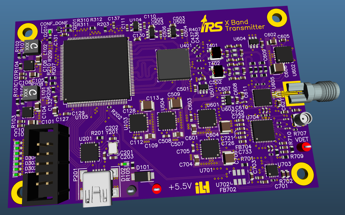
-
The biggest flaw in the head of a developer/software programmer.It's not about the quirks.
It's about the inconsistencies and KiCad is full of them.
Getting a good consistent GUI for multiple platforms isn't difficult, there are plenty of (free) examples out there that prove it.
Many people have said it before and I repeat it again; it's all about priorities.
Personally I would like to add that it's also about attitude.
With that I mean really listen to the community, people who have been working as a PCB designer for many years.
The developers of KiCad don't really seem to care about it.
Have you filed bug reports and wish list items at the Kicad Launchpad? Do you follow the developers' email listserv so you can see clearly what they are working on and why they've prioritized things the way they do?
The assertion that they don't care is not true.
This is not a bug, this is just fundamental understanding how to build up an intuitive piece of software.
Bit off topic, but I am completely convinced why most open source (not all!) totally fail in the long run because of this flaw.
Don't get me wrong, KiCad has a lot of potential, you can't deny that.
But the interface is made by and for programming geeks, NOT your every day, professional, I need a smooth interface that I can trust PCB user.
Most very good and professional PCB designers don't even know anything about programming or just the basics.
This kind of interface was an excuse 10 years ago maybe, but not anno 2018 anymore.
Yes I (and with me many others) have tried to talk to the developers and get involved.
But with an attitude that "we know it better, and we are not gonna do what all the big companies are doing, meh" you're not gonna make it.
Not to mention the overly sensitivity with every teeny bit of critique that is being given.
Everybody who feels the same and knows how to program, please contact me and I will have a look what we can do. -
The biggest flaw in the head of a developer/software programmer.It's not about the quirks.
It's about the inconsistencies and KiCad is full of them.
Getting a good consistent GUI for multiple platforms isn't difficult, there are plenty of (free) examples out there that prove it.
Many people have said it before and I repeat it again; it's all about priorities.
Personally I would like to add that it's also about attitude.
With that I mean really listen to the community, people who have been working as a PCB designer for many years.
The developers of KiCad don't really seem to care about it.
Have you filed bug reports and wish list items at the Kicad Launchpad? Do you follow the developers' email listserv so you can see clearly what they are working on and why they've prioritized things the way they do?
The assertion that they don't care is not true.
This is not a bug, this is just fundamental understanding how to build up an intuitive piece of software.
Bit off topic, but I am completely convinced why most open source (not all!) totally fail in the long run because of this flaw.
Don't get me wrong, KiCad has a lot of potential, you can't deny that.
But the interface is made by and for programming geeks, NOT your every day, professional, I need a smooth interface that I can trust PCB user.
Most very good and professional PCB designers don't even know anything about programming or just the basics.
This kind of interface was an excuse 10 years ago maybe, but not anno 2018 anymore.
Yes I (and with me many others) have tried to talk to the developers and get involved.
But with an attitude that "we know it better, and we are not gonna do what all the big companies are doing, meh" you're not gonna make it.
Not to mention the overly sensitivity with every teeny bit of critique that is being given.
Everybody who feels the same and knows how to program, please contact me and I will have a look what we can do.
Do you really think that the Kicad developers aren't also PCB designers? See, that's why I said you should actually join the developers' listserv to see what is actually going on and see who is actually doing the development. Because you don't know what you're talking about.
You say you've "tried to talk to the developers." Where? -
Don't know what I am talking about?
The biggest flaw in the head of a developer/software programmer.It's not about the quirks.
It's about the inconsistencies and KiCad is full of them.
Getting a good consistent GUI for multiple platforms isn't difficult, there are plenty of (free) examples out there that prove it.
Many people have said it before and I repeat it again; it's all about priorities.
Personally I would like to add that it's also about attitude.
With that I mean really listen to the community, people who have been working as a PCB designer for many years.
The developers of KiCad don't really seem to care about it.
Have you filed bug reports and wish list items at the Kicad Launchpad? Do you follow the developers' email listserv so you can see clearly what they are working on and why they've prioritized things the way they do?
The assertion that they don't care is not true.
This is not a bug, this is just fundamental understanding how to build up an intuitive piece of software.
Bit off topic, but I am completely convinced why most open source (not all!) totally fail in the long run because of this flaw.
Don't get me wrong, KiCad has a lot of potential, you can't deny that.
But the interface is made by and for programming geeks, NOT your every day, professional, I need a smooth interface that I can trust PCB user.
Most very good and professional PCB designers don't even know anything about programming or just the basics.
This kind of interface was an excuse 10 years ago maybe, but not anno 2018 anymore.
Yes I (and with me many others) have tried to talk to the developers and get involved.
But with an attitude that "we know it better, and we are not gonna do what all the big companies are doing, meh" you're not gonna make it.
Not to mention the overly sensitivity with every teeny bit of critique that is being given.
Everybody who feels the same and knows how to program, please contact me and I will have a look what we can do.
Do you really think that the Kicad developers aren't also PCB designers? See, that's why I said you should actually join the developers' listserv to see what is actually going on and see who is actually doing the development. Because you don't know what you're talking about.
You say you've "tried to talk to the developers." Where?
I just said that I (and other people) contacted them, or shared these stories multiple times.
So or you're not reading properly, or you're implying that I am lying?
Basically their answer is; wait until version 6 and we will see it from there. -
Basically their answer is; wait until version 6 and we will see it from there.
So basically you're complaining they're not going to throw out their existing development plan and progress to do things your way immediately? -
No?Basically their answer is; wait until version 6 and we will see it from there.
So basically you're complaining they're not going to throw out their existing development plan and progress to do things your way immediately?
I am complaining about a bad set of priorities.
Interface should be much higher on the list.
Things like schematic simulators, auto routers and 3D graphics are nice gimmicks, but without a proper user interface it's still not really usable.
Technically KiCad was working adequate from version 4, except for some minor bugs and quirks and other things (that could be done by 3rd party if really needed)
You can even see on their roadmaps were they spend time on.
They should have done this from the beginning.
Nail the user experience first, fix little bugs and things later.
The easy part; there are already a lot of competitors out there, so basically just copy their interface and you already know for sure that at least a big group of people can handle it easily.
(that's basically what they did with DipTrace)
Guess some people just like to reinvent the wheel -
I agree with b-force.
User experience and user interface need to be numbers 1 and 2 on the list of priorities.
This is what a lot of developers fail to understand. And they forgo huge chunks of potential market share because of it. -
And if they focused on the UI at the expense of everything else, they'd throw out a different section of the market. There are other tools out there with nicer UIs but they are not as flexible or powerful as KiCad. If the UI is that important to you then I suggest using one of the tools that has a more polished UI. The rest of us have managed to work around the UI issues in KiCad, it's just not a big deal.
I've used at least 5 or 6 different EDAs and they all had lousy interfaces, even one that cost thousands of dollars. KiCad is free and it does the job. Frankly I'd be annoyed if the UI changed significantly at this point because I'd have to spend time re-learning how to do things, time that I could instead spend making more boards. -
Frankly I'd be annoyed if the UI changed significantly at this point because I'd have to spend time re-learning how to do things, time that I could instead spend making more boards.
Would it be so bad to fix the fact that you hit "c" to duplicate something in the schematic editor, but Command-D to duplicate something in the PCB layout tool or footprint editor, but it's drag to select and then right mouse to duplicate to duplicate something in the parts library editor (or that you can drag to select and then copy block and when you immediately go to paste the block, you get an error message "Warning: No block to paste")?
If cleaning that up would hurt the usability of the tool for you, then KiCAD project really is stuck between a rock and hard place... -
And if they focused on the UI at the expense of everything else, they'd throw out a different section of the market. There are other tools out there with nicer UIs but they are not as flexible or powerful as KiCad. If the UI is that important to you then I suggest using one of the tools that has a more polished UI. The rest of us have managed to work around the UI issues in KiCad, it's just not a big deal.
Most of them have, that is correct.
I've used at least 5 or 6 different EDAs and they all had lousy interfaces, even one that cost thousands of dollars. KiCad is free and it does the job. Frankly I'd be annoyed if the UI changed significantly at this point because I'd have to spend time re-learning how to do things, time that I could instead spend making more boards.
But it's not a good argument to (therefore) do the seem thing.
At least with most other EDAs the user can change most of the interface to their liking.
And with most of the competitors the user can choice to work mostly with just keyboard shortcuts or only with the mouse or an hybrid..
This is fixed in KiCad and even many icons for certain tasks are completely missing.
Besides, if you read the KiCad 6 roadmap they even admit that the interface is not very logic and inconsistent.
I know it's not a very popular one anymore, but Ultiboard/Multisim is pretty good with their GUI
Easy to learn in just a couple of days and fully customizable.
I find it a bizarre way of working, the other way around.
Technically speaking an interface is also not the most difficult to program.
Like I said before, just basically copy what others did and improve/make it your own from there.
I find it cute to read that the current KiCad users really think they are a significant and representative amount of "the market ".
To be clear, I am not just talking about my personal preference, but what works for many people.
In a sense EDAs always have been very conservative to this compared to 3D CAD software, things like video editors or other sophisticated programs. -
Just my two cents. I worked with various EDA tools on hobby as well as on the professional basis. Now I use Altium at work and KiCad at home. I am allowed to use Altium for home projects too but it is not the point.
I want to make my designs available for others and any time and I don't want to shoot myself in the foot again. The thing is, that every single EDA I used for hobby (Diptrace, Eagle, CM) has some limitations. These are typically pins, nets or the PCB size. In the case of CM, it is very inconsistent library quality. I invested time in learning the package, creating libraries and then I hit the limit..
I may loose the access to Altium Designer when I change a job. How do I open my old projects then? Nope, I am not going to pay for Altium. It ain't that good.
Kicad can be an extremely frustrating software package but it is going to be there. I can keep it, I can use it. It does not have limitations perfectly set by the marketing department based on the data from "please help us improve our software" feature.
to the OP: Download Altium or better Orcad demo and create a board there. Then share your feeling about user-friendliness of the tool and also how likely you would pay 10k for it.
-
In fact, I am almost willing to fork the entire project and find a couple of motivated people to work just on the GUI until even my mom can work with it.
I recommend doing that. Then you will either a) create a much better tool or b) find out writing a much better tool is actually not that easy.
There are projects with similar goals you might want to help out, Horizon LibrePCB. There have been several other people promising to make a "better KiCad" but I don't think they got anywhere.
As the main developer of horizon EDA, I obviously beg to differ. I recently completed the PCB for my master thesis using horizon EDA: https://github.com/carrotIndustries/x-band-tx
Even though some features are still missing, it's perfectly usable for small to medium-sized projects.
Lukas, I am not happy seeing another EDA tool because I doubt that you will any bandwidth supporting it after you graduate and find a job but this is impressive.
-
Frankly I'd be annoyed if the UI changed significantly at this point because I'd have to spend time re-learning how to do things, time that I could instead spend making more boards.
Would it be so bad to fix the fact that you hit "c" to duplicate something in the schematic editor, but Command-D to duplicate something in the PCB layout tool or footprint editor, but it's drag to select and then right mouse to duplicate to duplicate something in the parts library editor (or that you can drag to select and then copy block and when you immediately go to paste the block, you get an error message "Warning: No block to paste")?
If cleaning that up would hurt the usability of the tool for you, then KiCAD project really is stuck between a rock and hard place...
Well that wouldn't personally bother me, because I select and shift-select-drag to duplicate everywhere and never even used C or Cmd-D but I agree it would be nice to have consistency there. I've been using it pretty heavily for almost 10 years now so I probably don't even notice many of the things new users complain about. -
I've tried to be patient with it, but its unusable. The user interface is just terrible (and I'm a professional software engineer). I finally lost it and uninstalled when I dropped a transistor om a schematic, tried to move it and had it leave part of the symbol behind (this is the latest 'stable' version as of the time of this post).
-
I've tried to be patient with it, but its unusable. The user interface is just terrible (and I'm a professional software engineer). I finally lost it and uninstalled when I dropped a transistor om a schematic, tried to move it and had it leave part of the symbol behind (this is the latest 'stable' version as of the time of this post).
If you are looking for a schematic package completely free of quirks like that you'll be searching a long time. Its amazing how reliable the production of boards can be when you consider the number of on screen quirks most software exhibits. -
I've tried to be patient with it, but its unusable. The user interface is just terrible (and I'm a professional software engineer). I finally lost it and uninstalled when I dropped a transistor om a schematic, tried to move it and had it leave part of the symbol behind (this is the latest 'stable' version as of the time of this post).
For something that's unusable quite a few of us are managing to use it just fine and have been for years. Good luck finding a similarly capable tool that doesn't have quirks. -
I've tried to be patient with it, but its unusable. The user interface is just terrible (and I'm a professional software engineer). I finally lost it and uninstalled when I dropped a transistor om a schematic, tried to move it and had it leave part of the symbol behind (this is the latest 'stable' version as of the time of this post).
Could you at least be a bit more detailed what is wrong here? A screenshot perhaps? I can not really deceiver what you experienced so your rant is not really useful at this point in time.
I have never seen KiCad leave parts of a symbol behind. And as far as I am aware this is even impossible with how symbols are implemented. The only things one can move independently are the text fields and that is on purpose as users want to be able to reposition them depending on their current needs. -
I've tried to be patient with it, but its unusable. The user interface is just terrible (and I'm a professional software engineer). I finally lost it and uninstalled when I dropped a transistor om a schematic, tried to move it and had it leave part of the symbol behind (this is the latest 'stable' version as of the time of this post).
How did you manage to do that? -
I am so tired of people shitting on KiCad. And I am pretty sure it is impossible to "leave half a symbol" by dragging it.
Kicad gui is absolutely fine. I turned on KiCad for the first time a bit over a year ago, and so far have completed multiple multi-layer and large multi PCB projects with no bugs. I found some great plugins like HTML BOM, or RF package that are just brilliant. I swear to god, people expect cad software to have a learning curve of social media smartphone app...
There are countless videos, tutorials, and about million shortcuts to do whatever you want. There are missing features of course, like clearance matrix etc...but that will come.
For what it does KiCad is up there with the best commercial CAD packages.