I got a reply from the manufacturer of my boards:
"Remove the non-functional pads on all internal layers is best, because it is reinforced adhesion of the hole copper ,and easy to drill process for the production,if remove the non-functional annular rings, you must be keeping the safety spacing 11mil(0.28mm) minimum to innerlayer copper for plating holes"
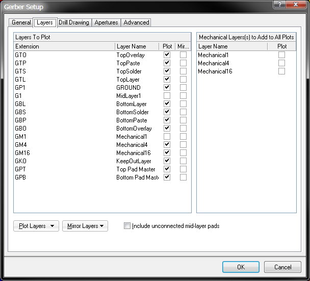
If i keep those rules in mind i gain no extra copper so ill just let my output job take care of it by deselecting 'Include unconnected mid-layer pads ' here:
On a sidenote: Wurth mentions this on here Multilayer FAQ:
"Due to manufacturing tolerances, in particular the dimensional variations of thinner cores, an adequate isolation distance of 225µm around the via drilling in design is recommended.
This ensures that the final product does not have isolation distances that are too small. Approximately, the same size is recommended if the pads on the signal inner layers, which are not connected, are removed."
So if i would be using Wurth boards i could actually gain 50um between two 0,15/0,45mm via's with 100um clearance and have 200um copper in between them instead of 150um on a 0.8mm BGA grid. So for future designs it could be useful to do this.


