The ADR3625 is a voltage reference with an output voltage of 2,5V. The ADR3630 (3V) and ADR3650 (5V) belong to the same family. The maximum current consumption is 90µA. The ADR3625 can source up to 70mA and sink up to 20mA. Analog Devices sells an A-grade and a B-grade. Unusually, the output voltage of the B-grade has the lower initial error with a maximum of 0,04%. The output voltage noise is specified as 7,5µVpp. The typical temperature drift is 2ppm/°C. With the A-grade, the value remains well below 3ppm/°C.

The datasheet contains a block diagram. It is very similar to the block diagram of the ADR3525. The only difference is that a large number of protection diodes have been added. While the ADR3525 datasheet refers to a special operating mode of the bandgap reference, there is no mention of this technology in the ADR3625 datasheet.
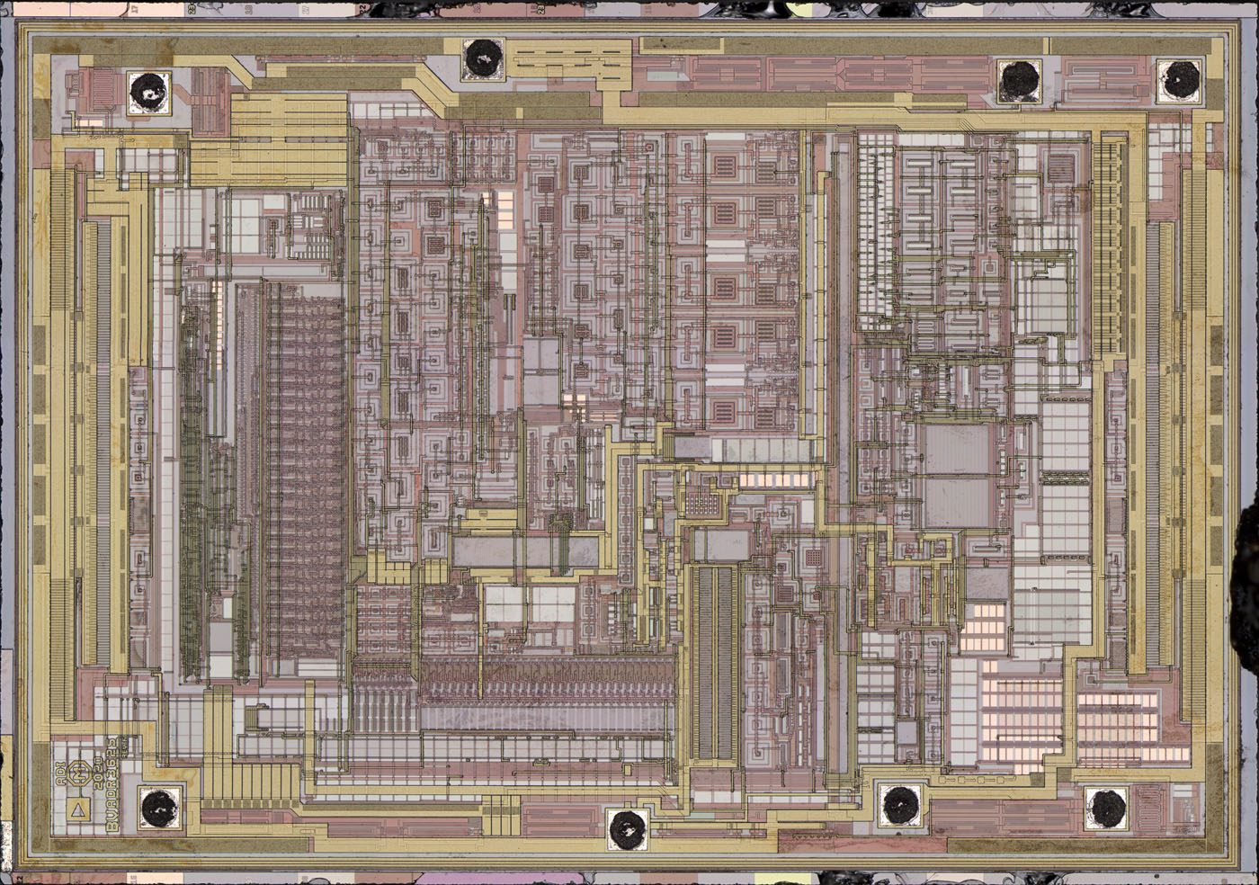
The die of the ADR3625 measures 2,20mm x 1,55mm, making it significantly larger than the die of the ADR3525.
This image is also available in a higher resolution:
https://www.richis-lab.de/images/REF01/54x03XL.jpg (37 MB)
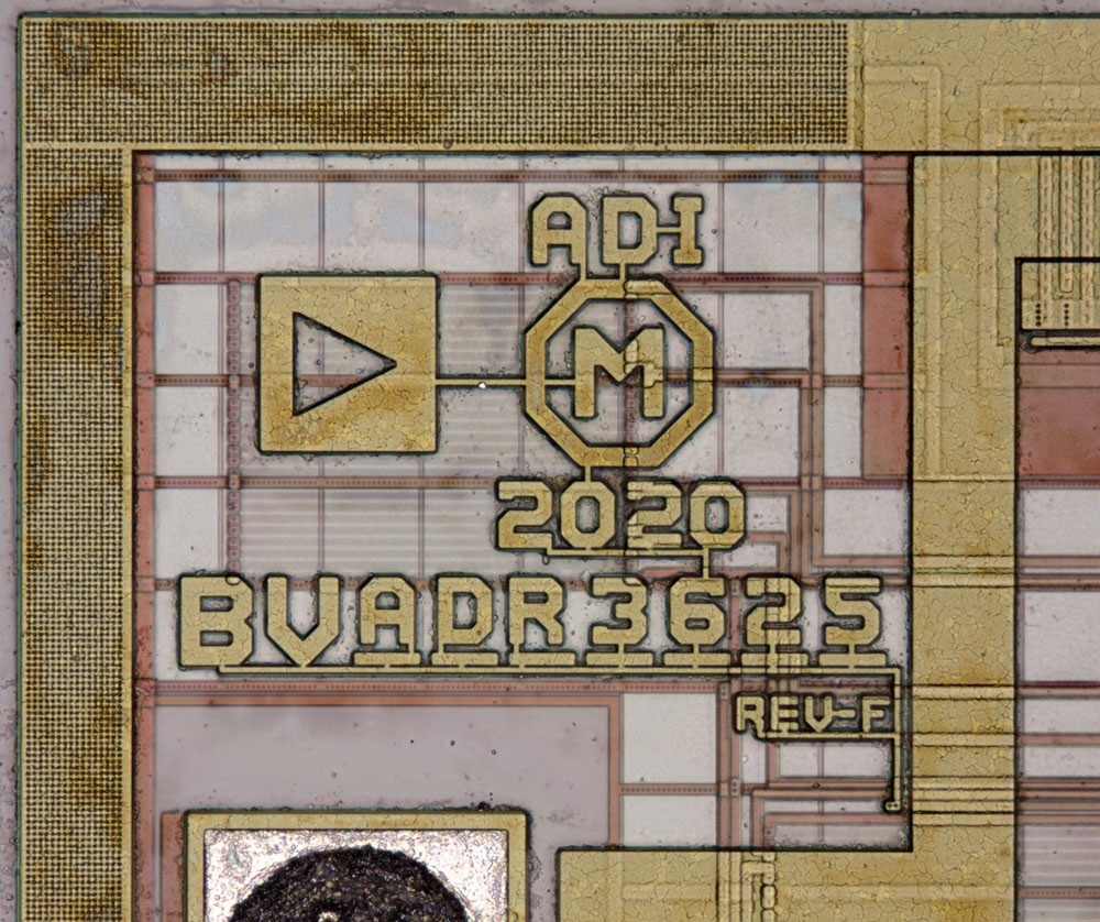
The design dates back to 2020. BV most likely stands for Beaverton, an American location of Analog Devices. The full designation ADR3625 is shown here. This could mean that the various output voltages are set via the metal layer. However, it is equally conceivable that the present design can represent all three output voltages and will be configured appropriately after production. REV-F shows that the circuit has been revised several times.
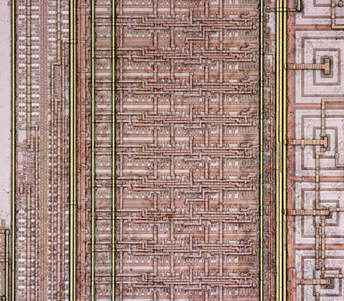
The letters and numbers are all connected to each other and even contact a deeper layer in the lower right area. This ensures that no errors occur due to electrically isolated islands during automated design checks.
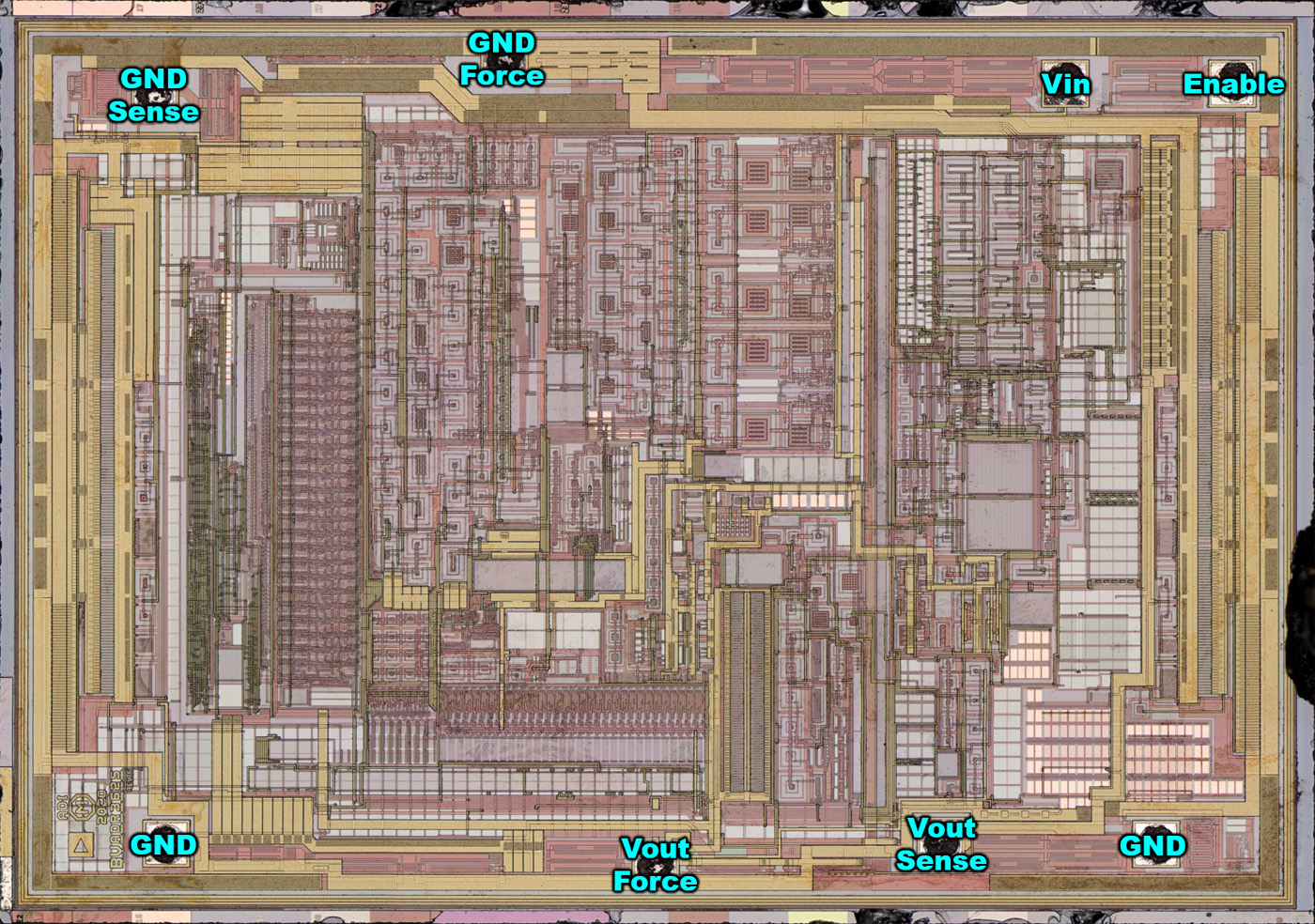
The circuit is quite complex and therefore cannot be analyzed in detail. However, it appears to be fundamentally different in design from the circuit in the ADR3525. The most striking feature is the output stage, which has been divided into two blocks. These blocks have been placed on the left and right edges. Due to the high output power of the ADR3625, a lot of power loss can occur in the output stages. By placing them on both edges, they heat up the die more evenly.
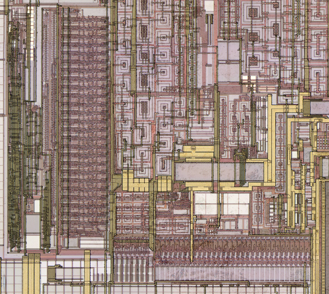
The ADR3625 datasheet mentions that it is configured using the DigiTrim process at the end of production. In the vertically arranged block shown here, you can see the circuit components of 25 fuses. To the left of this is certainly the control logic for this configuration option. The large horizontal block at the bottom edge appears to contain 32 switchable current sinks, thus representing a type of DAC. However, control lines to various other circuits can also be seen.
The circuit block with the fuses is reminiscent of the integrated circuit in the ADR3525, but is not completely identical to it.
https://www.richis-lab.de/REF49.htm 


