Author Topic: More voltage references - die pictures  (Read 44880 times)

0 Members and 1 Guest are viewing this topic.

Offline NoopyTopic starter

  • Super Contributor
  • ***
  • Posts: 1739
  • Country: de
    • Richis-Lab
Re: More voltage references - die pictures
« Reply #100 on: July 02, 2023, 07:46:20 pm »
...

Very interesting! Thanks for the extensive explanation!  :-+


I have one more: The MC1403 reference was developed by Motorola. According to the datasheet, it is comparable to the AD580 (https://www.richis-lab.de/REF28.htm). The output voltage is 2,5V with a tolerance of +/-25mV. The temperature drift is typically 10ppm/°C.


The datasheet of the MC1403 shows a temperature drift typical for a bandgap reference. The output voltage first rises and then falls again. ...but just up to 85°C.  ;)


The datasheet of the MC1403 contains a detailed circuit diagram. The designations of the transistors have been added here. This is the typical bandgap circuit. The multiple contacting of the 1kΩ resistor is a way of setting the temperature coefficient to a minimum.


The MC1403 uses just three pins of the package.


From the side, it is easy to see that the die was just partially cut and then broken out of the wafer.


The dimensions of the die are 1,3mm x 1,0mm.


Under a contact to the substrate one can guess a character string in some pictures. It seems there are the characters AP9.


The integrated circuit corresponds exactly to the circuit diagram. However, there is an unused bondpad in the upper right corner. In the lower right corner, this potential contacts a small structure that is connected to GND. It could be a pn structure that could be used for a temperature measurement.

The 1kΩ resistor is obviously adjustable, but also the 5,61kΩ resistor at the right edge offers possibilities to vary the resistance. Here, however, one has to adjust the mask of the vias. The metal surfaces are so large that they can reach the vias over a relatively large area.


The adjustable 1kΩ resistor has an unusual design. A simple resistor, a strip of the base doping, has been used. Underneath the resistor are 17 thin metal strips that were partially cut. Probably a laser was used here. The isolated square on the far left seems to have served to align the laser. A cut-out in the passivation layer is not visible. It was probably possible to cut the wires safely without such a cut-out.

The cut strips look somewhat dirty. This can be problematic if currents are still flowing through the debris. The behaviour of such areas can change over time and thus negatively influence the temperature drift of the reference.


The 30pF capacitor of the MC1403 is not immediately visible. It must be connected to GND on one side. The other side is connected to the collector of T6, the base of T4 and the collector of T2. No typical capacitor structure can be seen on the die. Consequently, the capacitance must be integrated in the areas of the active structures.

No larger capacitance is found in the areas of T6 and T2. This leaves just the transistor T4. A certain capacitance towards the substrate is formed by the buried collector of T2, which is a base contact for the transistor T4. This heavily n-doped layer rests directly on the substrate and has been extended from T2 to below T4 to represent the electrical connection between T2 and T4. However, this region alone does not represent 30pF.

As substrate PNP transistors, T4 and T5 just require an inner p-region and a surrounding n-frame. In cross-section, of course, it is not an n-frame, but an n-layer under the p-region. Although it would not be necessary, an outer p-region has been integrated here too. Most likely, the p-doping represents a large part of the 30pF capacitance. In contrast to the transistors T5, T6 and T2, T4 is not located in a n-doped well. As a result, the large p-doped area is electrically connected to GND and a capacitance is formed between the n-doped base area of the PNP transistors and the p-doped layer above it (green).


https://www.richis-lab.de/REF32.htm

 :-/O
 
The following users thanked this post: SeanB, Jim Narem, BU508A, RoGeorge, floobydust, alm, ch_scr

Offline NoopyTopic starter

  • Super Contributor
  • ***
  • Posts: 1739
  • Country: de
    • Richis-Lab
Re: More voltage references - die pictures
« Reply #101 on: July 08, 2023, 07:54:05 pm »


The above table from "Linear/Interface ICs Devices Data Vol. II" shows the voltage references that Motorola sold 1993. Beside the shunt regulator TL431 there is the LM385, the MC1403 and the MC1404. MC1403 and MC1404 are specified very similar. The MC1404 offers two additional functional pins and could be purchased with different output voltages: 5V, 6.25V and 10V.


In contrast to the MC1403, only a simplified circuit diagram is shown in the MC1404 datasheet. Accordingly it contains a typical bandgap reference.

Compared to the MC1403, the MC1404 in addition has the potentials Vtemp and Trim. The output voltage can be adjusted via the pin Trim. There is no application for the potential Vtemp. One could realize a temperature measurement with it. However, it does not seem to make much sense to use the core area of the bandgap reference for such additional functions.


The reference potential of the MC1404 is connected to the outside with two bondwires.


The dimensions of the die are 1,4mm x 1,1mm. In the upper right corner you can find the string BC5.


The circuit is quite clear. In the right area there are two unused PNP transistors.


As expected, the MC1404 is a classic bandgap reference. The core of the reference is built the same way as in the MC1403. The bias circuit is slightly different and there are some minor details.

In the MC1403 the bias current is generated based on the reference voltage. A JFET ensures a safe start-up of the circuits. In the MC1404, the JFET current source Q12/R11 generates the bias current out of the supply voltage. With this background, it seems only logical that the MC1404 compensates fluctuations of the supply voltage somewhat worse than the MC1403.

Above R5/R6 there is the transistor Q9, which is connected as a diode. The potential above the transistor is connected to the surface on which resistors R5/R6 are integrated. This probably was done to reduce leakage currents from the resistors.

In the supply of the current mirror Q7/Q8 with Q10 an additional diode path has been inserted. The capacitor C1 is integrated in the area around the transistors Q3/Q4 as on the MC1403.

The voltage divider R7/R8 is constructed with eight resistor strips. The symmetrical arrangement of R8 around R7 ensures that temperature drifts have a similar effect on both resistors. If you connect the resistors differently, you can set the different output voltages. This is achieved by varying the metal mask, in which the string 10V is shown too. The wide metal areas above the contacts allows a slight adjustment of the resistors and thus the output voltage. To do this, one has to change the mask for the contacts between silicon and metal.


The resistors R1 and R3 define the temperature drift of the reference voltage. As with the MC1403, the values of these resistors can be varied by modifying the contact mask.

The temperature drift is tuned at the resistor R2. As in the MC1403, metal leads were cut with a laser. An element for aligning the laser is shown in the upper left corner. Nevertheless, the laser was set very far down, so that it already has cut through the thicker areas of the leads. There is a risk that the resistive strip has been directly affected and these areas then change their behavior over time.


https://www.richis-lab.de/REF33.htm

 :-/O
 
The following users thanked this post: SeanB, Mickle T., Jim Narem, BU508A, RoGeorge, alm, ch_scr, iMo

Offline NoopyTopic starter

  • Super Contributor
  • ***
  • Posts: 1739
  • Country: de
    • Richis-Lab
Re: More voltage references - die pictures
« Reply #102 on: July 22, 2023, 07:57:20 pm »


This voltage reference was found in a Motorola Optobus transceiver (https://www.richis-lab.de/transceiver03.htm).


The metal layer reveals that it is a Motorola design. The internal designation is apparently C91J. The metal layer also shows that the output voltage is 2.5V.


The die offers a surprisingly large number of interfaces. Thus, the reference voltage can be tapped in the lower right corner and at the upper edge. Both interfaces additionally have a bondpad for a feedback of the voltage. As with the MC1404 reference voltage source, the bandgap potential Vtemp can also be tapped and the reference voltage can be adjusted via Vtrim.


The left part of the circuit is very similar to the MC1404. Just R3 and R4 have been added here. The output stage with the feedback to the bandgap reference is similar too. However, the output is much more robust. Q11/Q12 serves as a Darlington transistor and D3 represents a freewheeling diode.

The bias current generation and the current limitation at the output are much more complex than in the MC1404. The central block Q18-Q22 seems to generate a reference current which is fed into the circuit via Q13. If the voltage drop across R15 is too high, the bias current is diverted by the current mirror Q15/Q16 and thus the output stage driving current is reduced.

If you find a mistake let me know!


The resistors of the voltage divider R11/R13 are located in a field with eight resistor stripes flanked by two dummy structures. For the output voltage of 2,5V, just the two innermost resistor stripes are used. The other stripes are contacted but do not affect the voltage divider in this connection.


The four testpads in the left area activate up to four resistors that adjust the temperature coefficient of the reference voltage. The resistors consist of parallel connected strips with dummy structures and offer a ratio of 1:2:4:8.

In the right part of the image, you can see the transistor structures typical of a bandgap reference. Two larger, parallel-connected transistors (Q1a/Q1b) are placed above and below a smaller transistor (Q2). To the right of the center transistor are three resistor strips, two of which are connected in parallel and tied between the bandgap reference transistors (R3). The ideal value at this point is determined by the resistance of the voltage divider in the feedback loop (R13). Since the voltage divider can be adapted for different output voltages, it makes absolutely sense to adapt the resistors between the transistors accordingly.


The above table from the catalog "Linear/Interface ICs Devices Data Vol. II" shows the range of reference voltage sources that Motorola had in its program in 1993. None of them fits to the present circuit. The TL431 and the LM385 are shunt regulators. The MC1403 (https://www.richis-lab.de/REF32.htm) and the MC1404 (https://www.richis-lab.de/REF33.htm) are much simpler. Perhaps the voltage reference documented here is a special development that was never offered separately.


https://www.richis-lab.de/REF34.htm

 :-/O
 
The following users thanked this post: SeanB, Andreas, BU508A, RoGeorge, alm, ch_scr, iMo

Offline NoopyTopic starter

  • Super Contributor
  • ***
  • Posts: 1739
  • Country: de
    • Richis-Lab
Re: More voltage references - die pictures
« Reply #103 on: August 21, 2023, 03:52:04 am »


EDIT: For the latest analysis and information regarding the MAA550 take a look at the pictures and discription following the TAA550 in the next post.
« Last Edit: September 24, 2023, 07:12:17 pm by Noopy »
 
The following users thanked this post: SeanB, Mickle T., Andreas, doktor pyta, Jim Narem, BU508A, RoGeorge, ch_scr, iMo

Offline NoopyTopic starter

  • Super Contributor
  • ***
  • Posts: 1739
  • Country: de
    • Richis-Lab
Re: More voltage references - die pictures
« Reply #104 on: September 21, 2023, 08:15:42 pm »


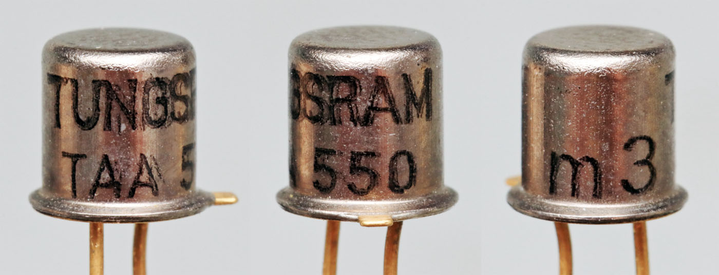
Ignore the MAA550 we had there will be an update soon. Here we have some new insights starting with a TAA550 from Tungsram. The development goes back to Valvo. One of the first advertisements promoting the TAA550 can be found in the magazine Electronics in December 1968. The TAA550 has been copied by many manufacturers over the years.


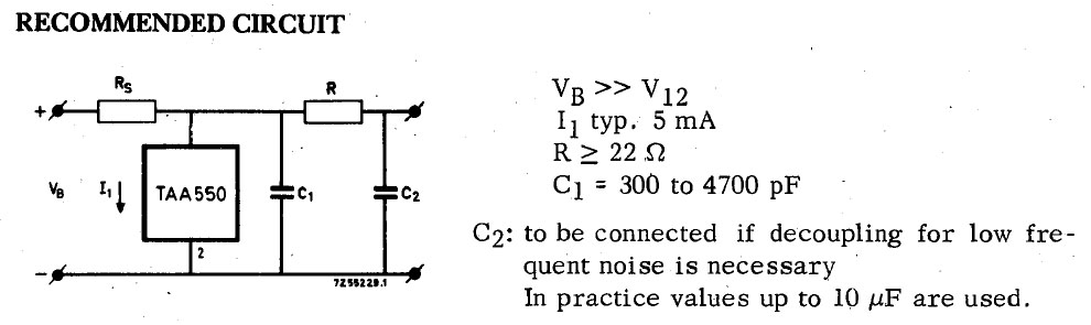
The application you can see here is taken from the "Philips Data handbook - Semiconductors and integrated circuits" published in March 1977. The filtering of the output is interesting. A CRC circuit is recommended instead of a simple capacitor. In an article in the magazine Electronics (December 1969), Valvo warns you shouldn´t connecting capacitors with more than 4,7nF directly to the output of the TAA550. Otherwise, in the event of a short circuit, oscillations between the line inductance and the capacitor must be expected, the negative voltages of which will damage the TAA550.


Due to the high reference voltage, the power dissipation that occurs in the TAA550 is not insignificant. The minimum required operating current is 2mA, 5mA is specified as a typical value. With this current, up to 175mW is generated. The datasheet shows that the typical current without heat sink is only permissible up to an ambient temperature of about 60°C.


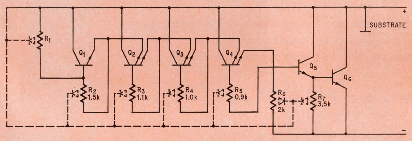
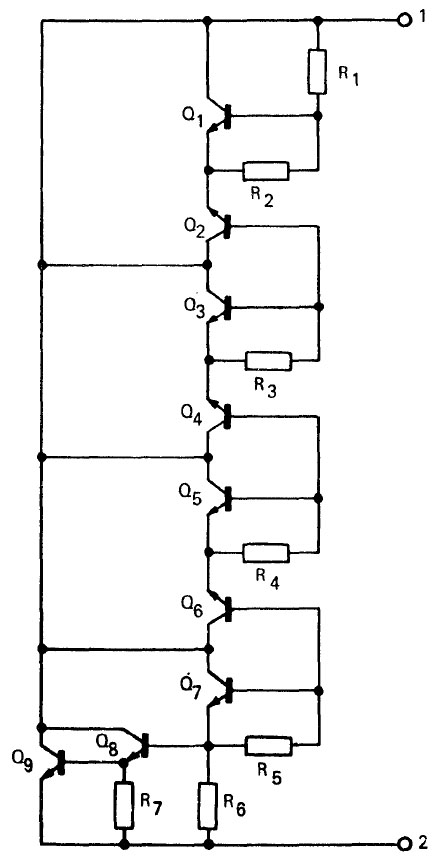
In the magazine Electronics from December 1969 (Volume 42) there is an article in which Valvo describes the construction and the functionality of the TAA550. There is also the above schematic shown, which at first sight seems very confusing.

An obvious and unusual feature of the TAA550 is the fact that the substrate is connected to the positive supply potential. Apart from special exceptions, integrated circuits in bipolar technology have actually always had the substrate connected to the most negative potential of the circuit.

The resistors are drawn with their parasitic diodes. In normal operation, these never become conductive. In the short circuit case described at the beginning, however, they are critical. Already at -1V at the TAA550 one has to expect high currents across the diodes.

The circuit contains three transistors with two emitters each. The functionality is not readily apparent with this illustration.


The above schematic is from the 1975/1976 SGS ATES Databook. Transistors Q8 and Q9 represent a Darlington circuit that adjusts the reference voltage by allowing more or less current to flow through the device. The reference voltage is the result of all base-emitter and emitter-base voltages of the circuit. Here, the transistors with the two emitters are each shown as two individual transistors. In one, the base-emitter path is operated in the flux direction (Q3, Q5, Q7), and in the other, it is operated in the reverse direction, acting as a Z-diode (Q2, Q4, Q6).

The transistor Q1 forms a so-called "Vbe multiplier" with the surrounding resistors. The circuit multiplies the base-emitter voltage so that about 1,9V drops across it. The voltage drop across the Darlington output stage is about 1,3V. The voltage drop across transistors Q3, Q5, Q7 is about 2,0V. Thus, the Z-diodes must have Zener voltages in the range of 8,3V to 10V. This is consistent with the article in magazine Electronics, where Valvo specifies an emitter-base breakdown voltage of 8-10V as a target.

As with many reference voltage sources, the positive temperature coefficient of the Z-diodes in the TAA550 is balanced by the negative temperature coefficient of pn junctions conducting in forward direction. However, the high reference voltage requires the somewhat more complex circuit.


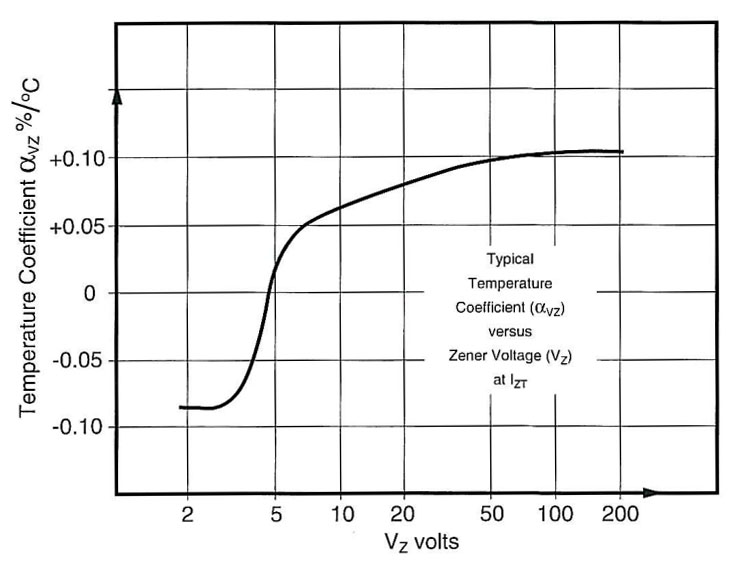
The temperature coefficient of a Z-diode depends on its Zener voltage. Microsemi shows the above behavior in its Micro Notes (203). From a Zener voltage of about 5V, the value becomes positive, whereby the temperature coefficient in this transition range also depends very strongly on the current. At 8-10V one would have to calculate with 0,055-0,065%/K (4,4-6,5mV/K). Assuming that the Z-diodes in the TAA550 behave similarly, they should bring a temperature drift of 13,2-19,5mV/K in total.

A single pn junction, on the other hand, offers a temperature coefficient of just -2mV/K. For this reason, in addition to the Darlington transistors Q8 and Q9, the circuit also contains the transistors Q3, Q5, Q7 working as diodes. This results in a total value of -10mV/K. The missing contribution is provided by the Vbe multiplier around Q1. It multiplies not only the base-emitter voltage itself, but also its temperature coefficients. With the previous estimation, the multiplier should be 1,6-4,8.


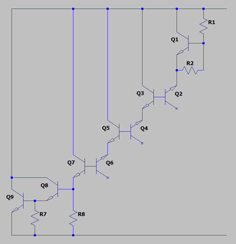
The purpose of the three R3, R4, R5 is not obvious at first glance. They are necessary because the special design of the TAA550 can lead to a problematic behavior. This becomes clearer if the circuit is drawn a little differently and simplified. Here you can see that the transistors Q3, Q5 and Q7 have the potential to behave like a chain of Darlington transistors. The current flow through the collectors would cause the transistors to saturate and there would be no longer a useful reference voltage.

To prevent this, resistors R3, R3 and R5 have been integrated. They sink the collector current and thus prevent it from becoming effective in the base-emitter junction. As the collector-base voltage and thus also the collector current increase downwards, the values of the resistors become smaller: 1,1kΩ / 1kΩ / 0,9kΩ.


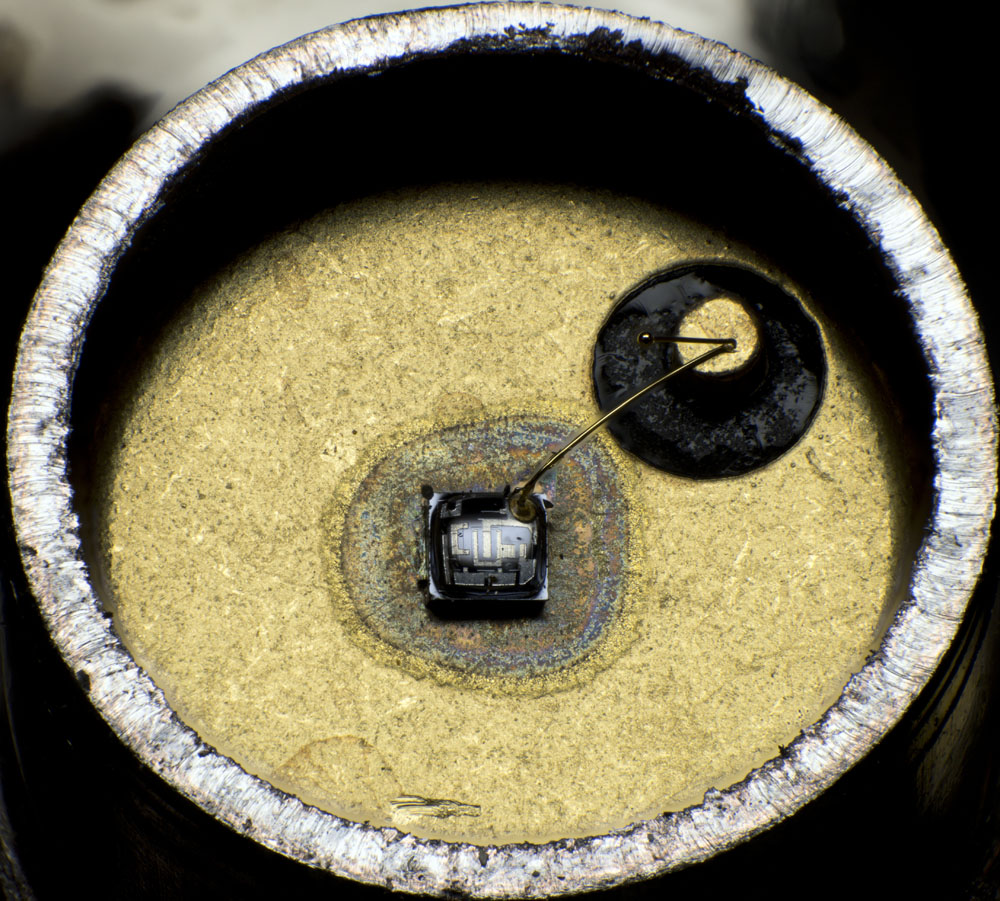
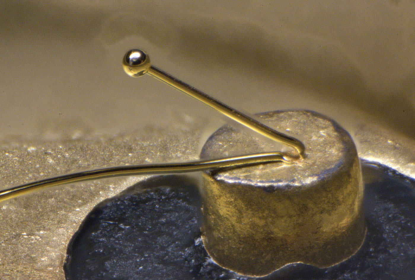
Here you can see the inside of the package. The end of the bondwire is strange. They left it quite long ending with a molten ball.


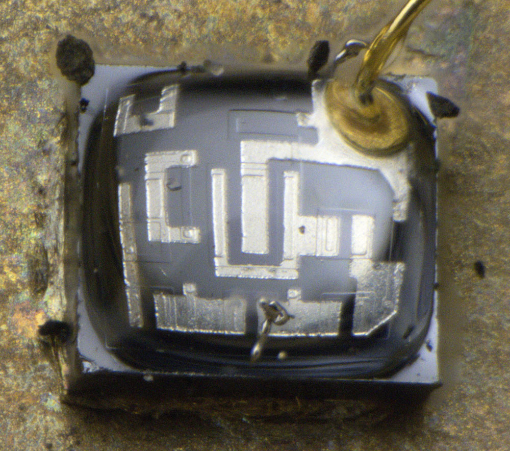
A transparent potting protects the die from environmental influences. It can be dissolved with paint stripper and then removed.


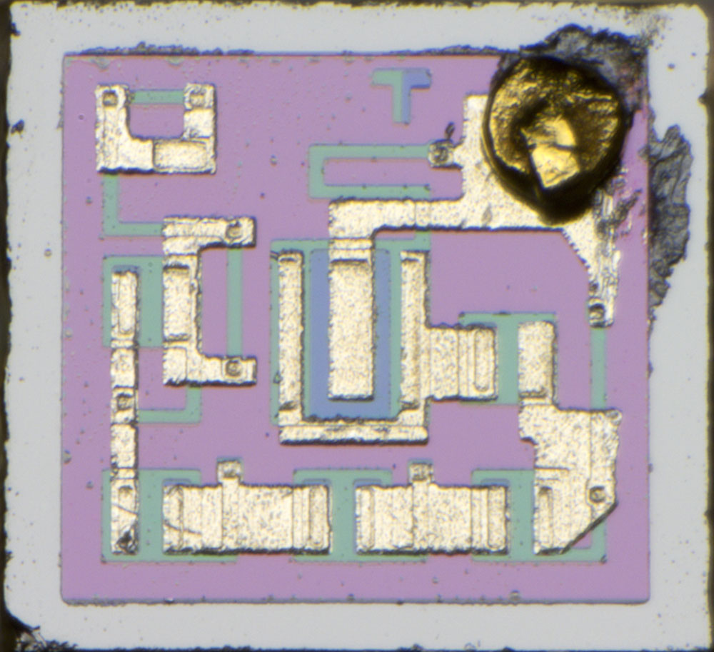
The edge length of the die is 0,55mm. Next to the bondpad is a T like Tungsram used as a logo. The typical dichotomy was implemented with the base and emitter doping. As a side effect, you can use the logo to see how well the two masks are aligned with each other.


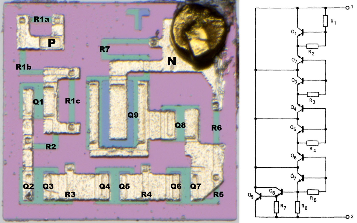
The most striking feature of TAA550 is the absence of isolated wells. All elements are located in the n-doped substrate. For this reason, the substrate here is connected to the positive supply potential via the package. In the upper left corner of the die is where the positive supply potential is fed into the circuit.

Q1, Q8 and Q9 are constructed like normal transistors except for the missing isolation to the substrate. The other transistors each have two blue emitter areas in the green base area. This can be seen especially well with the double transistor Q4/Q5. The output stage transistor Q9 is much larger to show a sufficient current carrying capacity.

The resistors R3 and R4 appear to be similar in size. R5, on the other hand, is noticeably smaller.


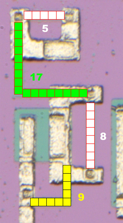
The resistor R1 consists of three elements. Depending on which multiplier you need for transistor Q1, you can bridge the resistors by changing the metal layer. However, this is not an individual tuning of one part. The manufacturing process must be stable enough that once the temperature coefficient has been set, it remains sufficiently constant through the batch. Roughly estimated, the multiplier can be adjustable in the range between 1,6 and 4,3. In this TAA550, the factor is  something around 2,9, which seems plausible.


https://www.richis-lab.de/REF36.htm

 :-/O
« Last Edit: September 24, 2023, 07:14:21 pm by Noopy »
 
The following users thanked this post: SeanB, Jim Narem, BU508A, RoGeorge, alm, ch_scr

Online RoGeorge

  • Super Contributor
  • ***
  • Posts: 6213
  • Country: ro
Re: More voltage references - die pictures
« Reply #105 on: September 21, 2023, 09:33:40 pm »
Funny looking that transparent potting.  8)
Makes one want to decapsulate a TAA550 and shine a LED at it, so to make a light-tuned voltage reference.  ;D

Offline NoopyTopic starter

  • Super Contributor
  • ***
  • Posts: 1739
  • Country: de
    • Richis-Lab
Re: More voltage references - die pictures
« Reply #106 on: September 22, 2023, 02:55:59 am »
Funny looking that transparent potting.  8)
Makes one want to decapsulate a TAA550 and shine a LED at it, so to make a light-tuned voltage reference.  ;D

Should be possible...  ;D

Online dietert1

  • Super Contributor
  • ***
  • Posts: 2077
  • Country: br
    • CADT Homepage
Re: More voltage references - die pictures
« Reply #107 on: September 22, 2023, 06:16:52 am »
Thanks for this interesting report.

Some days ago i was working on something similar, but i ended up using a "RefAmp" design (6.2 V zener + npn transistor) with a voltage divider (27K, 7K1) to make a temperature stable 33 V supply.

Regards, Dieter
 

Offline NoopyTopic starter

  • Super Contributor
  • ***
  • Posts: 1739
  • Country: de
    • Richis-Lab
Re: More voltage references - die pictures
« Reply #108 on: September 24, 2023, 07:09:17 pm »


Now lets take a new look into the Tesla MAA550, the reproduction of the TAA550. Here we have the first variant. FX stand for a production in May 1974.


The Radio Fernsehen Elektronik (13 / 1972) shows some further information about the MAA550. For example, it can clearly be seen that the MAA550 requires a bias current of at least 1mA. The specifications apply to a current of 5mA. At the same time, the text describes that the load from the connected circuit should not exceed 1mA.


The datasheet of the MAA550 contains the above circuit diagram. The operation is the same as the operation of the TAA550. Here the three transistors with the two emitters are shown as Z-diodes and normal diodes.


The dimensions of the die are 0,58mm x 0,57mm. As in the TAA550, no isolated areas can be seen.


Right below the bondpad is the contact to the substrate and thus to the P-potential. The resistor R1 consists of four elements which can be short-circuited via the metal layer. On the transistor T1 there is an unused contact. It is the base contact, which is not necessary, because the resistor R1d connects directly to the base area.

As in the TAA550, the diodes in the MAA550 are realized as transistors with two emitter areas. The three resistors R3, R4 and R5 are specified in the schematic with 800Ω each. If you look at the geometries on the die, you can clearly see that the lengths and thus the resistor values become smaller from top to bottom, as in the TAA550. The square output stage transistor T3 seems to be minimally smaller than the output stage transistor in the TAA550.


An estimation of the resistance values shows that the factor of the Vbe Multiplier can be set in the range between 1,6 and 4,0. With the metal layer we can see here, the factor is 3,4.


The MAA550 seen here was labeled in red. A datecode is not printed on the package.


The metal layer is severely damaged. On the center transistor at the lower edge, one contact is almost completely broken. Perhaps the device was thermally overloaded.


The MAA550 seen here carries the datecode BY1 and was thus manufactured in May 1977.


In the package there is a very badly damaged die. During production, the upper right corner was broken off. The metal layer shows clear signs of corrosion. The rest of the surface appears to be heavily soiled. It is hard to say what happened. Perhaps there were impurities in the package that attacked the surface over time.


https://www.richis-lab.de/REF37.htm

 :-/O
 
The following users thanked this post: SeanB, chickenHeadKnob, Jim Narem, BU508A, RoGeorge, ch_scr

Offline NoopyTopic starter

  • Super Contributor
  • ***
  • Posts: 1739
  • Country: de
    • Richis-Lab
Re: More voltage references - die pictures
« Reply #109 on: September 24, 2023, 07:10:24 pm »


This MAA550 is the second variant of the MAA550. It shows the datecode W5. It was therefore manufactured in May 1988. It is noticeable that the three MAA550 of variant 1 were also manufactured in May.


The connection of the bondwire with the pin does not appear particularly stable.


The edge length of the die is 0,49mm. One difference to the MAA550 variant 1 and to the TAA550 is immediately noticeable: Here the transistors are located in separated areas. This suggests that a common bipolar process was used. This would mean that the substrate is p-doped, the dark green areas are n-doped collector areas and the light green boundaries with a p-doping isolate the collector areas against each other.

However, since the positive potential is still connected to the substrate in the MAA550, the individual areas do not remain completely isolated. Current can still flow from the positive supply potential to the active elements through the junction. The junction acts like a diode in that place.


The first variant of the MAA550 has the same design as the TAA550. The second variant shown here differs not only in the basic construction, but also the circuit has been simplified. The three diodes and their parallel resistors are missing here.

The P potential is connected to the substrate via the package. At the upper edge, resistor R1 is connected to the frame structure. This means that the frame must be connected to the P potential. No structures can be seen under the frame. Presumably, the frame in the edge region contacts both the n-doped collector surfaces and the p-doped isolation frames and thus the substrate. This makes sense, since otherwise there would be diodes in all collector paths. However, these diodes would probably not affect the function.

Transistor T1 is clearly visible. D1, D3 and D5 are further transistors, but they are operated inversely and thus serve as Z-diodes. T2 is again connected as a normal transistor and drives the larger transistor T3, which contains three emitter areas.


Apparently, it was decided to represent the necessary negative temperature coefficient via the Vbe multiplier and the Darlington stage. Fittingly, the geometries of the resistors R1 and R2 show that their values were chosen differently than shown in the schematic. The ratio here is up to 31/6 instead of only 20/8, resulting in a negative temperature coefficient of up to -12.3mV/K, with the Darlington transistors -16.3mV/K.
Assuming the same temperature coefficients for the Z-diodes as for the TAA550 (13.2-19.5mV/K), the compensation range of the Vbe Multiplier should be sufficient.


The transistors, which work as zenerdiodes in avalanche breakdown, show the well-known luminous effect in contrast to the other transistors.


If you do not limit the current sufficiently, you can easily destroy the power transistor.


https://www.richis-lab.de/REF35.htm

 :-/O
 
The following users thanked this post: SeanB, chickenHeadKnob, Jim Narem, BU508A, RoGeorge, ch_scr, eplpwr

Offline NoopyTopic starter

  • Super Contributor
  • ***
  • Posts: 1739
  • Country: de
    • Richis-Lab
Re: More voltage references - die pictures
« Reply #110 on: September 27, 2023, 03:23:00 am »


The TAA550 seen here is supposedly from Philips, so it should be similar to the original development by Valvo.


The dimensions of the die are 0,55mm x 0,54mm. The structures basically correspond to the structures of the TAA550 built by Tungsram. The resistor in the upper left corner, which sets the factor of the Vbe Multiplier, consists of four elements. In contrast to other variants, in this TAA550 you can clearly see how the resistors for sinking the collector currents become smaller from transistor to transistor.


https://www.richis-lab.de/REF38.htm

 :-/O
 
The following users thanked this post: SeanB, Jim Narem, BU508A, RoGeorge, ch_scr, iMo

Offline NoopyTopic starter

  • Super Contributor
  • ***
  • Posts: 1739
  • Country: de
    • Richis-Lab
Re: More voltage references - die pictures
« Reply #111 on: September 30, 2023, 03:14:28 am »


I still have a few TAA550.  ;D

The marking on this TAA550 is unreadable. There might have been a logo to the left of the letters TAA550. The A at the end of the designation shows that here a binning was done.


In the package, quite a bit away from the die, there is a small element that is probably a remnant from the attachment of the die.


As with the TAA550 from Tungsram, the end of the bondwire has been left slightly long at the pin. The ball shows that the bondwire has been cut by melting it.


It shows that it is a design by Tungsram. Next to the bondpad is the specific logo that was also found in the TAA550 from Tungsram. The structures are also the same apart from minimal variations in the metal layer.


Compared to the TAA550 from Tungsram, however, the resistor of the Vbe Multiplier has been configured differently. Elements 1 and 3 are active. The optional short-circuit bridges can still be seen. In the Tungsram TAA550 just element 2 is active. If we use the values estimated there, the resistance factor in the Vbe Multiplier is 13/9, in contrast to the factor 17/9 in the right picture.


https://www.richis-lab.de/REF39.htm

 :-/O
 
The following users thanked this post: SeanB, Jim Narem, RoGeorge, ch_scr

Offline NoopyTopic starter

  • Super Contributor
  • ***
  • Posts: 1739
  • Country: de
    • Richis-Lab
Re: More voltage references - die pictures
« Reply #112 on: October 02, 2023, 03:14:08 am »


SGS ATES alternatively sold the voltage reference TAA550 with the name TBA271. The bin with the index B stands for an output voltage between 32V and 34V. The voltage range of the TBA271 extends overall from 30V to 36V.


Apart from details in the metal layer, the design corresponds to the design of the TAA550 built by Philips. It remains unclear what the small, electrically insulated element at the upper edge does. Perhaps it´s an auxiliary structure used in the manufacture of the chip.


https://www.richis-lab.de/REF40.htm

 :-/O
 
The following users thanked this post: SeanB, Jim Narem, RoGeorge, ch_scr

Offline NoopyTopic starter

  • Super Contributor
  • ***
  • Posts: 1739
  • Country: de
    • Richis-Lab
Re: More voltage references - die pictures
« Reply #113 on: April 10, 2024, 03:36:03 am »


A new TAA550!  ;D
The TAA550 shown here was manufactured by SGS.


The die was damaged during production. The fractures in the silicon crystal probably occurred during the cutting of the wafer and the parts fell off when they were inserted into the package.


It is the same design as in the TBA271 from SGS ATES. Here you can see that the insulated structure on the upper edge represents an F.


https://www.richis-lab.de/REF41.htm

 :-/O
 
The following users thanked this post: Jim Narem, RoGeorge, ch_scr, iMo

Offline NoopyTopic starter

  • Super Contributor
  • ***
  • Posts: 1739
  • Country: de
    • Richis-Lab
Re: More voltage references - die pictures
« Reply #114 on: April 21, 2024, 04:10:57 am »


There are still some TAA550 left.  ;D
The TAA550 shown here was produced by ATES and is therefore older than the TBA271 from SGS-ATES.


When the die was cut / broken out from the wafer, the left edge was damaged. There are characters on the lower edge which presumably represent an internal product designation.

This is the usual circuit found in many TAA550s and described in more detail with the Tungsram TAA550 (https://www.richis-lab.de/REF36.htm). However, the layout is different. The resistor in the top left-hand corner has one more contact, which allows the temperature coefficient of the reference voltage to be set more precisely.


https://www.richis-lab.de/REF42.htm

 :-/O
 
The following users thanked this post: Jim Narem, RoGeorge, ch_scr


Share me

Digg  Facebook  SlashDot  Delicious  Technorati  Twitter  Google  Yahoo
Smf